



If you want to find a company’s press releases, product details and short biographies of its key personnel, then its website is often very informative. But what you fail to find there are the details of the activities that led to the forming of the company – in fact, sometimes this information is nowhere to be found on the Internet.
That’s the case with IQE, which has just notched up 30 years in the epiwafer supply business. So when I went to interview one of its co-founders, CEO Drew Nelson, I was keen to hear how the venture got off the ground (see p. 20 for the full story).
When I spoke with Nelson, I found out that he met his cofounder, Mike Scott, at events associated with a government sponsored programme called the Joint Opto Electronics Research Scheme (JOERS). There Nelson would present work by BT, Scott would detail the latest successes at Plessey, and while this duo were together they would try to gauge the appetite for a supplier of InP epiwafers for the fibre-optic business. Talking to others in the industry, they knew they were on to a winner – they just had to convince an investor. Eventually they did so, with Shell Ventures, part of the Shell Group, providing funding.
Thirty years on, following a management buyout, a merger, a float on the stock exchange and the acquisition of a handful of other companies, IQE is the biggest epiwafer supplier in the world. It could hardly have gone better.
Judged in terms of compound semiconductor manufacturing in the UK, the company created by Nelson and Scott must be the biggest success right now. After all, in the intervening years, while IQE’s presence in this industry has grown, that of the likes of Plessey and BT has dwindled, despite their strong IP.
This clearly irks Nelson, and is behind his motivation to drive the formation of the world’s first compound semiconductor cluster. Pieces of this jigsaw are falling into place, and one of the most encouraging elements must be interest from overseas. Asian companies, described by Nelson as “fairly significant”, are starting to outsource their manufacture to the cluster.
Growth in this business will be great news for those at IQE. While they celebrate the thirtieth anniversary, they can get as much pleasure thinking about the promise of the future as the triumphs of the past.
After a quiet period due to the saturation of the mobile handset industry, the GaAs wafer market is waking up, according to a new resport by Yole Développement (GaAs Wafer and Epiwafer Market: RF, Photonics, LED and PV Applications report, July 2018). It forecasts a 15 percent CAGR between 2017 and 2023 (in volume), with an impressive 37 percent, especially for photonics applications.
As one of the most mature compound semiconductors, GaAs has been ubiquitous as the building block of power amplifiers in every mobile handset. In 2018, GaAs RF business represents more than 50 percent of the GaAs wafer market. However, market growth has slowed down in the past couple years due to the handset market’s gradual saturation and shrinking die size.
“At Yole, we expect GaAs to remain the mainstream technology for sub-6 GHz instead of CMOS, owing to GaAs’ high power and linearity performance as required by carrier aggregation and MIMO technology,” explains Hong Ling, Technology and Market Analyst at Yole. Since 2017, GaAs wafer has been particularly notable in photonics applications. When Apple introduced its new iPhone X with a 3D sensing function using GaAs-based lasers, it paved the way for a significant boost in the GaAs photonics market. The GaAs wafers market segment for photonics applications should reach $150 million by 2023. “GaAs-based ROY and infrared LED applications have also caught our attention”, asserts Ezgi Dogmus, technology and market analyst at Yole. “We estimate, 2017-2023 CAGR achieves 21 percent (in units) for the total GaAs LED market, surpassing more than half of the GaAs wafer volume by 2023.”
In terms of the wafer and epiwafer businesses, each application requires a different size and quality when determining wafer and epiwafer prices. As a new entrant, photonics applications will impose new specification requirements compared to the well-established RF and LED wafer and epiwafers, creating significant ASP diversity.
From a value chain point of view, the GaAs photonics market’s remarkable growth potential will offer plenty of opportunities for wafer, epiwafer, and MOCVD equipment suppliers, as well as for investors.
Sumitomo Electric, Freiberger Compound Materials, and AXT, involved in GaAs wafer supply, lead the market with about 95 percent of market share collectively. And since new laser applications have very high specification requirements for GaAs wafer that are constantly evolving, Yole analysts’ expect the top players to maintain their technical advantage for at least another 3 - 5 years.
Regarding GaAs epiwafer production, Yole’s analysts identified different business models. The GaAs LED market is principally vertically integrated, with very well-established IDMs like Osram, San’an, Epistar, and Changelight. In parallel, GaAs RF businesses outsource significantly from well-established epihouses.
Within the GaAs photonics market, the epi business is still applicationsdependent. GaAs datacom market segment is mostly epi-integrated, with dominant IDMs like Finisar, Avago, and II-VI. For 3D sensing in smartphones, epi outsourcing is significant. In 2017, Apple’s supplier Lumentum used IQE as its VCSEL epi supplier. This resulted in an almost 10-fold increase in IQE’s stock price. Other leading GaAs epihouses are in qualification or ramping up. Yole expects the photonic epiwafer market to behave similar to the GaAs RF epiwafer market.
Kaiam, a manufacturer of data centre optical transceivers, has initiated a strategic transceiver reserve programme. The strategic reserve is intended to protect US and European data centres from the effects of the incipient US-China trade war.
The Trump administration has recently enacted broad-based tariffs that could impede the importation of Chinesemade optical transceivers into the US. Because US Cloud data centre companies are largely dependent on a supply of Chinese-made transceivers, they are highly vulnerable to collateral damage from the increasingly turbulent US-Chinese relationship. As one of the few remaining US optical transceiver companies, Kaiam is immune to illeffects of US-China trade tensions. Kaiam is building a strategic reserve of transceivers that its customers can draw down in response to a dwindling Chinese transceiver supply. The company will populate this reserve with units fabricated in its UK facility and welcomes partners to add to this reserve.

“In today’s global economy, it’s easy to assume goods will flow seamlessly across borders indefinitely. We sometimes forget that the optical components that power Cloud companies like Google, Facebook, Amazon, and others are virtually all made in China and are thus susceptible to trade tensions. As patriots, we believe a transceiver reserve is necessary for our domestic security,” said Jeremy Dietz, VP of global sales and marketing at Kaiam. “Our advanced technology and manufacturing process allows us to easily build a buffer to protect our nation in case of an embargo or even a natural disaster. We are currently exploring secure underground locations in states such as Utah and Nevada.”
“Our constitution implicitly guarantees the fundamental right to engage in online activities ranging from the sublime to the abject on a 24/7 basis,” said CTO Rob Kalman of Kaiam. “We view it as our patriotic duty to protect these rights, for it is more true than ever that the price of freedom is eternal vigilance!”
The Compound Semiconductor Applications Catapult, Wales’ first and the UK’s newest Catapult has announced that it will open its Innovation Centre, based in South East Wales, in early 2019. The announcement made by Secretary of State for Wales Alun Cairns, also confirmed that the Catapult will receive £51 million of grant funding from the £780 million investment in the UK’s internationally renowned Catapult network announced by the Chancellor Philip Hammond as part of the Government’s industrial strategy. This builds on the £180 million announced by the Prime Minister last month for centres in the North East last month, taking the total of additional funding to almost £1 billion.
The Catapult has already employed 23 people and is set to create around 100 new jobs internally. By 2023 it aims to have helped create 1,000 new hightech jobs within the businesses it has supported around the whole of the UK. With analysts predicting that the world market for compound semiconductors will increase from $66 billion today to over $300 billion by 2030, it is essential that the UK plays a substantial part in that growth and the Catapult is here to help make that happen. Secretary of State for Wales Alun Cairns said: “This investment in the Compound Semiconductor Applications Catapult cements Wales’ reputation as a leader in advanced electronics. Bringing together academics and businesses to develop new technologies will support areas of our daily lives from the next generation 5G mobile network to improving scanning at airport security.
“Our investment in this technology will help Welsh businesses exploit a hugely lucrative global market and ensure that Wales continues to lead the world in science and innovation, creating vital new jobs along the way.”
Compound Semiconductor Applications Catapult CEO, Stephen Doran said: “Our Catapult is a UK-wide centre, based in Wales. With immediate effect, this grant funding will allow the Catapult to create a critical mass of industry-leading expertise at the heart of the world’s first compound semiconductor cluster in South Wales. The transformative potential for compound semiconductors to meet the challenges of the future has never been higher, and our new Innovation Centre will make sure that Wales is at the forefront of this revolution.”
The Catapult Innovation Centre will house a design studio, laboratories and test facilities, supported by simulation and modelling tools and advanced capabilities. It will help companies to accelerate the development of new products using compound semiconductors.
The Compound Semiconductor Applications Catapult has also set out its strategy with the publication of its Launching the Compound Semiconductor Applications Catapult brochure which was developed in collaboration and with input from over 150 companies in the sector. The strategy focuses around three areas: the Catapult’s new Innovation Centre; designing and manufacturing a series of evaluation modules to help companies prototype systems; and running a series of challenge programmes to identify how best compound semiconductors can address global challenges.
The Catapult is actively looking to fill positions across all levels of the organisation and in particular its three technology areas: Power Electronics, Photonics and Microwave and RF. Working with the Catapult can provide the opportunity to contribute and shape a business in its early stages with the stability of secured funding within which to operate. The Catapult has a collaborative, supportive and inclusive culture which will be reflected in its Innovation Centre where agile workspaces and settings for different types of working behaviour are part of its DNA. The Catapult has the benefit of a fast-moving entrepreneurial culture and a strong financial footing.
Network firm Infinera has announced its intent to acquire Coriant, a privately owned network company, to create one of the world’s largest optical network equipment providers.
The combination positions Infinera to capitalise on the next wave of global network spending as network operators transform their networks to transition from 4G to 5G, from Optical Transport Network (OTN) to packet and from closed to open network architectures. Infinera’s vertically integrated business model provides the ability to unleash value for customers and investors as the company’s combined network solutions power the world’s largest network operators. Ovum forecasts optical network spending to reach $17.8 billion in 2022. Under the terms of the definitive purchase agreement governing the acquisition, subject to customary adjustments, Infinera will pay approximately $150 million in cash at closing, and estimated additional amounts of $25 million in the two quarters post-closing and $55 million over a period of years. Infinera will issue approximately 21 million shares, which when combined with the cash consideration, results in total transaction consideration of approximately $430 million.
“Acquiring Coriant is a fantastic opportunity, strengthening our ability to serve the world’s largest network operators, accelerating our ability to leverage vertical integration and reinforcing our commitment to our long-term business model,” said Tom Fallon, Infinera CEO. “This powerful combination immediately benefits our combined customers by delivering the innovative technology required for the next wave of network spending.”
The acquisition is expected to be substantially accretive in 2019. This accretion will come from $100 million of identified cost savings in both cost of goods sold and operating expenses. Total cost synergies of $250 million are expected through 2021, with the continuation of operating synergies and the introduction of vertical integration into the Coriant product line, resulting in a step-function increase in Coriant’s margins. Infinera will be acquiring a debt-free balance sheet and expects cash flows to pay back transaction consideration within three years.
Coriant invested nearly $1 billion in research and development over the last five years to significantly advance its portfolio to address the growing demand for software automation and open, disaggregated platforms. Infinera recently upgraded its portfolio based on the innovative Infinite Capacity Engine (ICE4). Combining the strengths of both companies creates a powerful new portfolio to support our customers’ transition from 4G to 5G, from OTN to packet and from closed to open network architectures.
Confident in the combined company’s opportunities, Coriant’s majority owner, Oaktree Capital Management, expressed an interest in being compensated for this transaction largely in stock. Post-transaction, Oaktree will own approximately 12 percent of the combined company on a fully diluted basis. Pursuant to the terms of the definitive purchase agreement, Oaktree has agreed to lock up 50 percent of its shares for six months post-close and the remaining 50 percent of its shares for 12 months post-close. To fund the cash requirements of this transaction, and to support future working capital requirements, Infinera plans to pursue debt financing. Morgan Stanley Senior Funding has committed to provide debt financing for the transaction, subject to customary conditions.
The acquisition is expected to close in the third quarter of 2018, subject to customary closing conditions. The board of directors of Infinera has unanimously approved the transaction. Morgan Stanley & Co. LLC served as financial advisor and Wilson Sonsini Goodrich & Rosati, PC served as legal counsel to Infinera on this transaction. Moelis & Company served as financial advisor and Kirkland & Ellis served as legal counsel to Coriant.
Industry analyst firm N-tech Research has just published a new report titled Micro-LED Market Opportunities: 2018-2027 that forecasts the global micro-LED market will grow from $2.7 billion in revenues in 2019 to $10.7 billion in 2022.
N-tech believes micro-LED technology is making substantial advances, which will produce substantial opportunities in the coming years from applications such as near-eye AR/VR projectors and automotive head-up displays which require a combination of small form factor, low weight, super-high resolution and super-high brightness. The smart watch market is another opportunity for micro-LEDs. Here, the combination of extremely low power consumption and very strong brightness make micro-LEDs an obvious choice for wearable displays. N-tech sees this segment as generating $1.6 billion in 2022. Growth is also expected in extralarge displays. Such displays are used in video walls, digital cinemas, digital signage and home theatres, where N-tech believes they will greatly benefit from the scalability of micro-LED technology to large areas (already demonstrated by Sony and Samsung). Micro-LEDs also offer the ‘giant screen’ sector the possibility of hybridisation with other functionalities, and compatibility with flexible and transparent display designs.
Micro-LEDs are not for everyone. N-tech believes that there are still applications where micro-LEDs will struggle to make inroads. These include smartphones, tablets and regular TV market, where LCD and OLED technologies will continue to do well. Benefits from micro-LEDs are not as apparent in these markets although low power consumption could be something of a selling feature for tablets and smart phones.
The Poweramerica Institute at North Carolina (NC) State University, a member of Manufacturing USA, has awarded funding to six new member projects that will enhance wide bandgap technologies in the US. In addition, PowerAmerica has awarded funding for 20 projects to be led by existing members for a total of $20 million in project funding for this cycle. The new member projects receiving funding are:
Wide bandgap power modules for next generation systems
GE Aviation Systems and National Renewable Energy Laboratory (NREL) will work together to design and produce advanced wide bandgap power modules made with SiC and GaN. The goal of this project is to enable true engine coolant temperature-grade equipment which is required to support next generation defence systems as well as commercial transportation, wind and solar, while reducing overall system costs.
Dual-inductor hybrid converter for direct 48V to sub-1V DC-DC module
A team at UC Boulder will design and implement a GaN-based, novel converter with an increased density of ten times that of converters currently on the market, with up to three times lower power loss. The converter will have fewer components, simpler implementation and lower cost. It can be used for power delivery to data centres, cellular base stations, portable applications, and defence systems.
Devices for solid-state circuit breaking at the medium voltage level
A team at the University of North Carolina, Charlotte (UNCC) will test a functioning prototype of a medium voltage (3.3 kv) SiC solid-state circuit breaker. The use of SiC in the product will enable fast turn-off capability in the microsecond range or better, and superior efficiency compared to silicon. Market segments to be targeted include utility operators of the electricity distribution network.
600V GaN bi-directional switch
Infineon will develop a low-cost, 600V bidirectional 70 mΩ switch based on the company’s CoolGaN HEMT technology, capitalising on the unique bidirectional nature of the GaN HEMT. The project will validate both the dual gate concept and a solution for substrate voltage stabilization, and will make the GaN switch more economically attractive compared to the standard silicon devices commonly used today.
Graduate wide bandgap semiconductor power device lab
A team at NCSU will establish a graduate laboratory course focused entirely on the design, fabrication, and characterisation of wide bandgap power devices, and disseminate the curriculum to PowerAmerica members to accelerate the education of new engineers.
Power electronics teaching lab incorporating wide bandgap switches and circuits
Researchers at UNCC will develop a modular, multi-function, educational highfrequency power electronics board with plug and play capability. The new board will give students the flexibility to perform different power electronics lab sessions and train undergraduate students as wide bandgap power electronics engineers through hands-on experience and practical knowledge of WBG semiconductors in power electronics applications.
PowerAmerica aims to save energy and create US manufacturing jobs by accelerating the development and large-scale adoption of wide bandgap semiconductor technology made with SiC and GaN in power electronics systems. The institute, located at North Carolina State University in Raleigh, NC, is funded by the Department of Energy, industry partners and the state of North Carolina, and has a member portfolio representing more than 45 companies in the wide bandgap semiconductor field.
France-based GaN-on-silicon device pioneer Exagan has delivered transistors and switching ICs for pocket-sized fast chargers
As the dust settles on this year’s PCIM Europe, myriad power electronics companies are taking home a vast array of GaN-based devices.
For example, GaN Systems showcased 100 V and 650 V GaN E-HEMTs, Transphorm unveiled 650 V GaN FETs while EPC demonstrated its low-voltage enhanced-mode GaN FETs, targeting automotive, power supply and data centre applications, and more.
At the same time, France-based Exagan, also a key power electronics player, launched its 650 V G-FET power transistor alongside an integrated driver and transistor switching system, G-DRIVE, aimed at fast charger markets.
Described as being easy to design into electronic systems, the products are compliant with the USB power delivery 3.0 type C standard. And as Exagan president and chief executive, Frédéric Dupont, puts it: “The market potential here is enormous, including portable electronic devices as well as homes, restaurants, hotels, airports, automobiles and more.”
“In the near future, users will be able to quickly charge their devices by plugging a standard USB cable into a small, generic mobile charger,” he adds.
Since spinning out of CEA-Leti and Soitec in 2014, Exagan has firmly focused on developing 650 V GaN-on-silicon products for photovoltaic, automotive and PC markets and more. So why focus on the charging market right now?
According to Dupont, silicon power devices simply cannot fulfil fast charging applications, opening the door to GaN-based systems. But moreover, the chief executive reckons his company can deliver more intelligent and cost-effective GaN device solutions for this application.
“This is a place where GaN can really have a play, but the challenge is the cost and providing a complete solution – this is why you won’t see many GaN players addressing this segment,” he says. “However, Exagan can bring a lot of value here in the short-term.”
Indeed, thanks to a rich heritage of heteroepitaxy development from France-based CNRS-CRHEA, CEALeti, and Soitec, Exagan has been ahead of the pack on production, and consequent costs, from word go.
During processing, a stack of buffer, insulating and strain management layers is deposited between the silicon substrate and GaN epilayers to relieve crystal stresses and prevent cracking.
As a result, Exagan has been able to take GaN-onsilicon FET fabrication to larger wafer sizes, focusing on 200 mm production at X-Fab’s CMOS foundry in Germany, as many other GaN players grapple with smaller, 150 mm wafer sizes.
“Most companies are at six inches today but we have been working at eight inch, which is a good size for GaN,” points out Dupont. “This is important for costs, as most of the silicon power electronics market is currently being manufactured at eight inch... and we are using the same 200 mm CMOS infrastructure and equipment.”
“In the future we will see some silicon power devices moving to twelve inches but we think GaN will stick with eight inches,” he adds. “I don’t want to say forever but certainly for a long time as the cost structure is already very competitive.”
Costs aside, Dupont is also certain that GaN-based systems are ideal for fast-charging applications. As he points out, heteroepitaxial devices, such as GaN-onsilicon FETs, are fabricated as lateral devices.
“Compared to vertical SiC devices, these transistors are suited to integration and co-packaging,” he says. “So while SiC devices are very suitable for high current and high power applications, GaN is a good choice for fast charging applications and, indeed, any application that can benefit from system in package integration.”
“We have always believed that GaN should be approached as a system solution, rather than a transistor solution, this is why we are offering our intelligent GaN Power solutions to the market” he adds.
And for the future, Dupont says Exagan will be focusing on co-packaging silicon driver ICs with GaN transistors to achieve the best combination of cost, performance and functionality, rather than integrating the driver electronics onto the GaN transistor chip to produce a monolithic IC.
“Customers want to have a whole solution, not just a transistor,” says Dupont. “And they also want to know how to drive it, how to control it, how to design a transformer and so on.”
“We have to make sure our products have what a designer needs for a particular application... and many customers want to use an external silicon driver, this is why we developed the G-FET,” he adds. “Meanwhile, some customers and applications need a more integrated solution, and this is offered with G-DRIVE.”
Right now, Exagan is sampling and finalizing application development of G-FET and G-DRIVE products with its customers and will ramp production with foundry partner X-Fab according to demand. The company is also working with TÜV NORD’s aerospace and electronics arm, HIREX Engineering, on device testing and qualification in a range of applications.
“The power electronics industry has been very conservative about new technologies, but wide bandgap materials – both SiC and GaN – are revolutionizing this space,” says Dupont. “I do hope in a few years you will have a small GaN-based charger in your wallet, that can charge your phone, laptop, and anything you want to charge.”
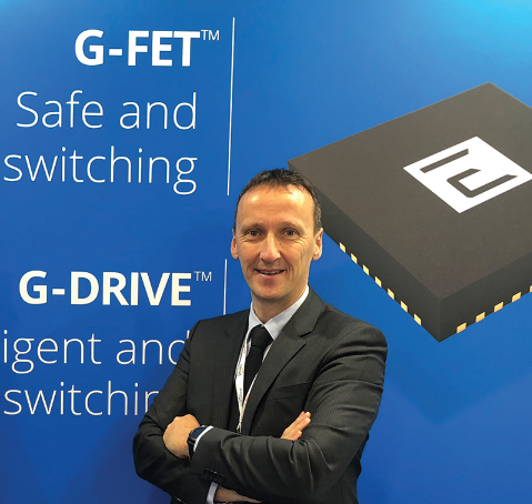
Exagan chief executive, Frédéric Dupont, believes the fastcharger market holds massive potential for GaN FETs and systems.
GT Advanced Technologies opens a crystal growth facility to meet imminent silicon carbide market boom, reports Rebecca Pool
In June this year, US-based GT Advanced Technologies, opened a state-of-the-art SiC manufacturing plant in Hudson, New Hampshire.
Equipment, including crystal furnaces, has been shipped over from the company’s former Merrimack facility, sold in December 2016. And as GTAT chief executive, Greg Knight, puts it: “Merrimack was designed for a very different business so we’re now at Hudson, which has been designed from the ground up for this business.”
“The facility is designed to be north of 100,000 square feet of crystal growth production,” he adds. “The first batch of furnaces are already installed and are producing crystal. In the past we have installed thousands and thousands of furnaces so this is very much a known entity for us and we intend to ramp production very quickly.”
GTAT has been producing crystal-growth equipment for the photovoltaics industry, as well as honing SiC boule production, for several years. Emerging from bankruptcy following a disastrous sapphire furnace supply contract with Apple in 2014, the company set out to establish a stable, high-yield robust 6-inch process for SiC boules for photovoltaic, electric vehicle, data centre markets and more.
The current process includes the company’s ‘SiClone’ SiC sublimation furnace and full SiC seeds, and Knight is confident the resulting six-inch boules compete with 4-inch versions on quality. What’s more, the chief executive is certain his company and process is ready for a SiC device market that is poised to explode.
“We believe that the demand for silicon carbide will truly start to accelerate around 2021 to 2022, so in my mind, now is the time to enter the market,” he says. “The market is still far from this inflexion point, when you see volumes ramping, but we are entering at scale and will add incrementally as utilisation rises.”
“We can respond very quickly to utilisation, which is important as you don’t want to outpace yourself and end up with a factory that’s say, 30 percent utilised,” he adds. “But we will be able to be a major player as the market gets through the inflexion point and reaches true volumes.”
Crucially, Knight hopes to soon establish a robust supply chain for SiC markets, providing low-cost, highly repeatable crystal growth equipment that can be easily scaled with a ‘fairly low’ capital outlay. He is confident that GTAT’s experience in crystal growth processes and furnace production, combined with managing supply chains, gives it a competitive edge in meeting the growing demand for wide bandgap semiconductors.
At the same time, however, Knight also wants to ensure GTAT doesn’t compete with its customers.
As he puts it: “One of the largest problems in the silicon carbide industry today is that the substrate providers are also the main competitors to their customers.... and we don’t think this is a long-term strategy that is particularly healthy for the industry.”
Given this, GTAT will grow the SiC crystal and then sell it to vertically integrated customers that can fabricate wafers and devices. “We’re also aligning with strategic partners, which include the pure play wafer manufacturers that will also take our crystal and fabricate epi-ready wafers that can be distributed into the market,” he adds.
6-inch production
Right now, GTAT manufactures 6-inch silicon carbide materials, but as Knight points out, the company is ready to transition to 8-inch production when volumes demand the larger wafer size. Importantly, the chief executive reckons the new facility is ready and can make this leap without any additional capital outlay.
“Fabs in Asia, including China, are focused on four-inch wafer sizes while European and US fabs are working with six-inch wafers, and are looking towards eight-inch sizes,” says Knight. “Such high-end fabs are running on eight-inch silicon and larger, and are currently using their equipment on a downsized six-process, so moving to eight-inch wafer sizes will not require new capital for most of the Western fabs.”

Importantly, as part of its roadmap, GTAT will also focus on reducing costs. Right now, the selling price of a 6-inch SiC wafer comes in at between $1200 and $1500, but Knight reckons these figures will drop to $1000 in the near future.
“Our costs can bring [today’s] selling price down significantly and we believe that in a few years we will have the crystal component cost of a wafer – not including additional process steps – to below $300,” he says. “We really have to get the epi-ready wafer costs down to a point where you can get mass adoption into the end markets.”

The roll-out of 5G will draw on advances in RF and optical semiconductor technologies, basestation system architectures and network topologies by Tony Fischetti from Macom
Much has been written about the impending global roll-out of 5G wireless infrastructure. This is expected to have a transformative impact on everything from mobile device connectivity and fixed-wireless services to transportation, industrial and entertainment applications and beyond. By combining data rates that could be ten to a hundred times faster than those of today with the capacity to handle untold data traffic volumes, the global 5G network is anticipated to provide connectivity that is almost instantaneous, alongside a seemingly limitless bandwidth elasticity that will encompass people, autonomous vehicles, IoT devices, industrial systems and civil infrastructure.
Before large scale deployment of 5G can begin, daunting technology and regulatory issues will have to be resolved. These challenges have an upside, however – they present a tremendous opportunity for operators to evolve network infrastructure in a sustainable manner that enables continuous improvements in bandwidth, power, management and cost efficiencies, amid an ever-intensifying data deluge. Consequently, the advent of 5G invites a fresh, top-to-bottom look at global communications infrastructure, from RF and optical chips to base station system architectures and network topologies.
It is certainly no coincidence that the efforts at developing 5G are paralleling an evolution in civil radar, which is used for air traffic control and weather surveillance. Efforts at streamlining and improving radar infrastructure are informing commercial 5G technology and deployment strategies. That’s not surprising, given that the end goals of these civil and commercial initiatives are similar: the creation of a scalable, cost-effective and highly integrated antenna technology that enables faster, more accurate and more sensitive transmit and receive capabilities. For civil radar, this ensures an expanded field of ‘view’ to aircraft and weather systems, while for 5G, it increases subscriber coverage.
In the US, both efforts are supported by government sponsored, cross-agency planning and coordination.
The aim is to consolidate national radar infrastructure into a single multifunction platform, while freeing up valuable radio spectrum for reallocation to commercial 5G wireless services. This programme, known as Spectrum Efficient National Surveillance Radar (SENSR), brings together the Federal Aviation Administration (FAA), the National Oceanic and Atmospheric Administration (NOAA), the Department of Defense (DoD), and the Department of Homeland Security (DHS).
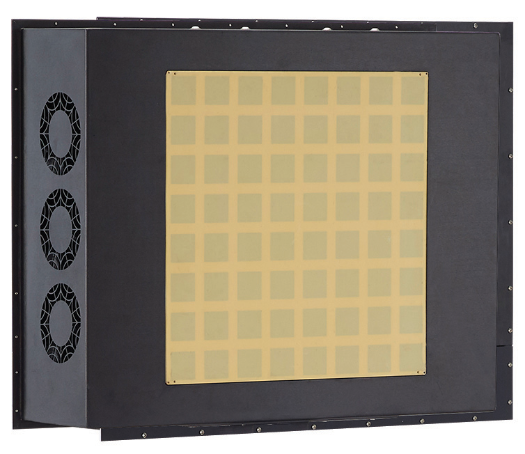
MACOM Scalable Planar Array (SPAR) Tiles
Drawing on civil radar
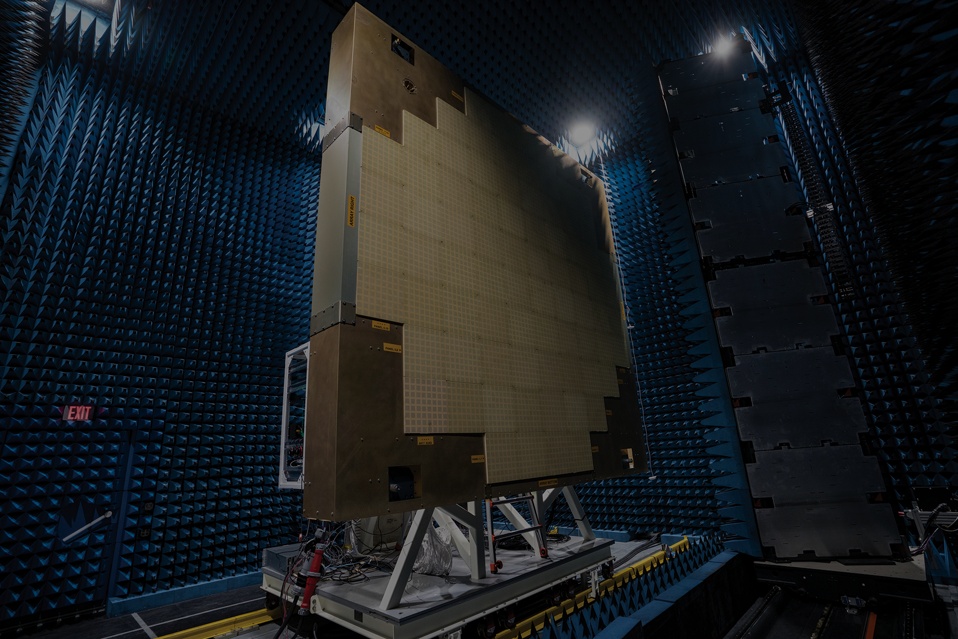
One of the recent developments in radar antenna has been the introduction of tile-based, planar phased-array radar for air traffic control and weather tracking applications. This breakthrough provides a compelling template for the architecture and assembly of massive MIMO (multiple-input, multiple-output) 5G systems. Drawing on the highly-integrated antenna sub-systems, and volume-scale commercial packaging and manufacturing techniques, will allow those associated with the roll-out of 5G to take little time in building planar arrays that can be flexibly tailored and scaled for deployment across a wide range of environments. And this will be at one-fifth of the cost of that for conventional array architectures, as demonstrated by the first-generation of Scalable Planar Array (SPAR) Tiles targeted for civil applications.
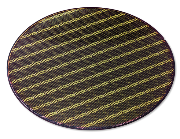
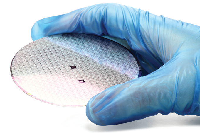
A MACOM 8-inch silicon wafer provides cost efficiencies at scaled volume production
A downside of the current generation of conventional, mechanically-steered air traffic control radars is the slow revisit rates, due to gimbal axis rotation. Planar phased array radars address this weakness with electronic scanning via stationary arrays comprised of hundreds to thousands of transmit and receive elements. What’s more, planar arrays are readily equipped to track weather patterns and unmanned aircraft systems, in addition to conventional aircraft. Thanks to this universality, numerous radar functions are integrated into a single, cost-effective multifunction platform.
It is expected that 5G massive-MIMO antennas will adopt a similar architecture to their radar-based cousins. That means that the number of transmit and receive elements will expand well beyond the two to eight antennas found in current MIMO configurations, and extend to anywhere from 64 to hundreds of antennas.
Similarities between planar air-traffic control radar arrays and 5G basestations don’t stop at the antenna architecture layer. Both feature a coherent beam forming capability, whereby each transmit and receive element in a massive-MIMO array operates in concert with others. This is highly beneficial, dynamically increasing transmitted power and receiver sensitivity in the direction of subscribers, while mitigating noise, interference and reflections from other sources. In densely populated areas, this approach overcomes bandwidth and capacity limitations, while mitigating multipath problems.
Another virtue of coherent beam forming massive-MIMO is that, by leveraging digital phased arrays, it can outperform traditional fixed-beam massive-MIMO architectures in terms of latency, wide band performance and the use of multiband antennas. The upshot is a superior spectral efficiency, which holds the key to wider coverage areas and a higher quality of service for a greater number of subscribers, at a lower cost of implementation.
Advances in GaN and MMICs
It is not just the evolution in basestation architectures and beam forming techniques that is aiding the deployment of 5G infrastructure. There are also improvements in semiconductor and packaging technologies that are offering compelling advantages over legacy approaches.
For massive MIMO, antenna configurations have to be tightly clustered, creating a need to preserve available PCB space, particularly at higher frequencies. One way to address these constraints is to switch from 5G basestation designs that use discrete ICs and single function MMICs to those that employ multifunction MMICs.
In addition to the space saving advantages provided by multifunction integration, costs can be trimmed by reducing individual die packaging, design complexity, testing and assembly labour. Meanwhile, reductions to the number of interfaces can increase overall mechanical reliability.
With all these factors at play, mainstream adoption of GaN-on-silicon is coming at just the right time. Thanks to scalability to 8-inch and 12-inch wafers, this technology is poised to provide cost efficiencies that are well out of reach for GaN-on-SiC at scaled volume production levels, while delivering performance metrics that can’t be achieved with LDMOS.
The superiority over LDMOS is significant – power efficiency is more than 70 percent higher, power per unit area is higher by a factor of four to six, and there is scalability to higher frequencies. In parallel, comprehensive testing data has affirmed the capability of GaN-on-silicon devices to conform to stringent reliability requirements, and to replicate and even exceed the RF performance and reliability of rivals made from GaN-on-SiC.
Where GaN-on-silicon clearly has the upper hand over GaN-on-SiC is in its potential to integrate increased functionality at the silicon level. This yields additional space optimization, leading to ultra-compact MMICs; and it enables the homogeneous integration of GaN devices and CMOS-based devices on a single chip. The latter opens the door to multifunction, digitally assisted RF MMICs that incorporate on-chip digital control and calibration, on-chip power distribution networks, and more.
Superior switches
RF switches – either in the form of discrete components or front-end modules, where they are integrated with LNAs and controllers – will play a pivotal role in 5G wireless basestation performance. There are a wide variety of underlying semiconductor technologies to select from, and designers need to select the best semiconductor junction for the required system function, while keeping an eye on conserving valuable real estate and minimising power loss and associated costs. Insertion loss is a critical performance metric: every tenth of a dB gained in insertion loss performance translates to extended range and expanded subscriber coverage.
For front-end transmit/receive topologies in highpower 5G antennas, extremely low insertion loss can be realised with AlGaAs and heterolithic microwave IC (HMIC)-based switch technologies. Supporting high-frequency operation to enable wider bandwidths, these technologies may help to maximize received sensitivity and antenna coverage while maintaining transmit/receive signal integrity. In addition, by lowering power loss, these technologies may lead to less compensation further down the RF signal chain.
To give an example of these benefits, a discrete heterojunction AlGaAs p-i-n diode switch can halve the high-frequency insertion loss compared to other switches in its class. This advantage translates to a more reliable system performance at higher frequency bands.
Optical opportunities
To handle the massive increases in network data traffic that lie ahead, emerging 5G network architectures are expected to rely more heavily on high-speed optical interconnects from the network backbone through to baseband processing, and on to the antenna. This architecture, which we refer to as fibre-to-the-antenna, reduces copper cabling as new fibre deployments push deeper into the network.
Wireless fronthaul is a prime example of how innovations in optical semiconductor and packaging technologies – at optimal cost structures – have the potential to transform today’s wireless network topologies, which could extend from remote radio units to baseband units.
We anticipate new 100 Gbit/s, single-wavelength PAM-4 DSPs and advanced silicon photonics technologies to provide high-performance, cost effective 100G optical interconnects for centralized/cloud radio access network architectures. This will greatly simplify the design and maintenance of remote radio units, with processing intelligence moving to a centrally managed, maintained, and cooled baseband unit, which services a multitude of remote radio units over long distances.
Previously, the common public radio interface protocol enabled a streamlining of centralized/cloud radio access network architectures, but data delivery speeds fell short of the mark. Bridging this gap is 100G connectivity in cloud data centres, a move that has resulted in a reduction in 100G cost structures. Wireless operators are now well positioned to exploit the speed and cost efficiencies of 100G interconnects for wireless fronthaul in preparation for the 5G data deluge, while enabling a flexible centralized/cloud radio access network architecture designed for seamless scalability into the future.
The parallel advances in RF and optical semiconductor technologies, basestation system architectures and network topologies are converging to propel the wireless networking industry toward the realization of more elegant, integrated and cost effective wireless infrastructure on the path to 5G connectivity. Drawing on innovative technologies honed in the civil and commercial technology domains, system designers and network architects are well equipped to realise higher levels of functionality, performance and device integration for 5G network infrastructure while streamlining data flows throughout the network, from core to antenna.
Back in 1988, Drew Nelson fulfilled a long-held dream by launching his own company. Thirty years on, it could have hardly turned out better: IQE is the world’s biggest epiwafer supplier, with facilities on all three major continents; and it’s the driving force behind the creation of the world’s first compound semiconductor cluster Richard Stevenson reports
At the beginning of 1980s, companies making InP chips for the fibre-optic industry had a broad range of expertise. Their skillsets included the design of the device, its testing, and its production – including the most challenging aspect of all, the epitaxial growth of the heterostructure.
But in 1988, this situation changed irrevocably. From then on, those chipmakers could choose between adopting a vertically integrated approach, or outsourcing epitaxial growth to a new start-up. Now known as IQE, this epitaxial specialist launched under the name Epitaxial Products International (EPI), reflecting its desire to serve a global industry.
Over the last thirty years the company has increased in size, to have manufacturing facilities on all three major continents; and it has expanded its portfolio, by diversifying its range of epiwafers, and adding substrates and material technologies to the mix. What’s more, it has become the driving force behind the development in the world’s first compound semiconductor cluster, which is making much headway in South Wales.
At the helm of the company since its formation is its co-founder Drew Nelson. After gaining a doctorate at Sheffield University – where he developed microwave devices, grown by LPE and MOCVD – in 1981 he joined British Telecom, where he led a group developing epitaxial technologies for detectors, lasers and modulators. But that was never going to be his long-term career – he had always wanted to run his own company.
The spark for fulfilling this dream came through his involvement in the Joint Opto Electronic Research Scheme, an initiative sponsored by the UK government. This programme, which focused on developing the technology for optoelectronic applications such as fibre-optic networks, brought many of the nation’s biggest technology companies, such as BT, Plessey, GEC and STC, together with several smaller organisations and universities.
Through JOERS, Nelson met Mike Scott, who shared his vision for launching a supplier of epiwafers. “We gauged the level of appetite, and we were encouraged to set up the business,” says Nelson.
Nelson had no intention of going to his bosses, to see if BT would fund this venture: “It definitely wasn’t the right culture.” Instead, he crafted a business plan with Scott and tried to secure backing from venture capitalists. “It wasn’t easy at times, but eventually we were put in touch with Shell Ventures.”
This introduction led to funding from Shell Ventures, a part of the Shell Group that had been created following encouragement by the then Prime Minister, Margaret Thatcher.“
She basically said to them, you’ve gained a huge amount of revenue from North Sea oil, and you should plough some of that back into British technology. We ended up being their keyhole on the semiconductor industry.”
Coming to Cardiff
Backed by “a couple of million pounds”, Nelson and Scott decided to build their facility on a brown-field site on the outskirts of the Welsh capital, Cardiff.
“The Welsh Development Agency were the premier agency in the UK industry for attracting inward investment, and we were able to get some capital grants to help the company,” says Nelson.
That wasn’t the only benefit of this particular location, however: the Electronic Engineering Department at Cardiff University had tremendous expertise in building and testing lasers. “We thought that would be a good source of skilled labour and engineers.”
Once the fab had been built, it was kitted out with equipment to grow and characterise epiwafers. While MOCVD tools were by no means as advanced as they are today, at least they didn’t have to be home built.
“We could have systems built for us, to our very specific designs, which we did,” recollects Nelson. “So we started with one MOCVD system from Thomas Swan, and one MOCVD system from CVT.”

His Royal Highness, the Duke of Edinburgh (right), unveils a plaque to mark the opening of the extension to IQE’s St Mellon’s facility.
Substrates were sourced from AXT, and some suppliers in Japan. “Two-inch substrates were the norm, and even at BT we had been using even smaller substrates than that,” says Nelson. One of the benefits of the JOERCs initiative is that it helped to create a UK manufacturer of metal-organic source materials, Epichem. EPI used this supplier, which had commercialised some of the technology developed at Queen Mary University of London.

IQE CEO Drew Nelson shows His Royal Highness, the Duke of Edinburgh an MOCVD reactor during a visit at the start of the millennium.
To characterise the epiwafers, Nelson and Scott invested in microscopes to assess morphology; X-ray diffraction tools to determine crystallinity; and an electrochemical capacitance-voltage tool, known as a post-office profiler, to determine the doping levels in the epilayers. A home-built photoluminescence kit enabled the evaluation of the optical properties of the epiwafers.
As the facility took shape, Nelson and Scott started to put a team together, while securing their first orders. “I looked after the technology and production side of things, and Mike was more focused on sales,” explains Nelson.
Winning the first orders is never easy, particularly if the business is global. For EPI, they needed to target companies in Japan, as many of them were at the forefront of InP optoelectronics. To this end, EPI employed a local agency. This move paid dividends, with good sales obtained through them adding to successes in the US and Europe.
Initially, EPI only produced material for optoelectronic applications – principally detectors, modulators and lasers. But it did not take long before the portfolio broadened, first with the addition of InP for microwave systems, and then a family of GaAs products: initially lasers, then HBTs and pHEMTs.
These new products gave the industry a broader choice of suppliers of GaAs epiwafers. EPI now offered an alternative to: the French start-up PicoGiga, which had been offering merchant epi since 1983, and specialised in GaAs pHEMTs for direct broadcast TV; and to Quantum Epitaxial Designs (QED) of Bethlehem, PA, that started producing GaAs pHEMT and MESFET epiwafers in 1989.
EPI grew quite quickly throughout the early 1990s, while broadening its product base. “We ended up getting some pretty big contracts, and companies,” remarks Nelson. “We were recognised as the expert company for InP-based materials.”
As epiwafer sales blossomed, fortunes for the company’s backer, Shell, declined. All the big oil companies that had diversified in the 1980s went through a lean patch, leading them to focus on their core business. This led to a management buy-out of EPI, funded by a bank loan and company cash.
Rising sales continued through the 1990s, and by the end of the decade EPI needed to expand its capacity to fulfil demand. “The route to that was a stock market listing,” explains Nelson. “We also wanted to make sure that we were capturing as much of the wireless market that was emerging. So we negotiated a deal to join forces with Pennsylvania based QED.”
Floating in the summer of 1999 at $12.50 per share on the EASDAQ, the European version of NASDAQ, the new venture raised $70 million. This provided much needed funds for capital equipment for the Cardiff and Bethlehem facilities.
The new entity needed a new name. To come up with one, management quizzed staff for ideas by running a competition. The winning entry came from putting EPI and QED together, and taking letters three, four and five: IQE.
Nelson says that the merger was one of “roughly equals”. However, EPI owned 55 percent of the shares, and with IQE listed in London, it made sense to have the headquarters in Cardiff. Due to this, IQE’s core of the management team were those that had led EPI.
At the turn of the millennium, sales were flourishing, with the company continuing its drive to expand its business. It bought UK substrate supplier Wafer Technology, and set up a new facility, IQE Silicon. Situated right next to its Cardiff fab, this arm focused on the growth of silicon and SiGe.
Bursting the bubble
Good times rarely last forever. And they didn’t at IQE. Rising revenue had been fuelled by the rapid growth of the fibre optic industry, and when this went into rapid decline – associated with the well-documented bursting of the dot.com bubble – sales of InP wafers plummeted from around £3 million per month to just £300,000.
“We had to lay off a lot of staff,” remarks Nelson. “It’s always painful to lay off staff when you have recruited and trained them. But we did everything we needed to survive.”
In these tough times, IQE started to lay the foundations for the success that followed. Valuations for all III-V firms had fallen massively from giddy heights, and the time was ripe for further acquisition.
In 2006, IQE acquired the epi business of Emcore; the following year it bought MBE Technologies of Singapore; and in 2012 it acquired the epi business of RFMD.
“We ended up being consolidators of the industry,” says Nelson. “That gave us scale, which was critical, and gave us the biggest customers in the industry.” These customers were confident in working with IQE, because they knew it would be a long-term deal; and they valued the multi-site manufacturing, as this mitigates risk. From IQE’s perspective, more facilities enabled higher volumes, and greater purchasing power with its suppliers.
Further acquisitions and investments have broadened the portfolio. In 2009, the buying of NanoGaN of Bath, UK, added technology for realising high-quality GaN; purchasing Galaxy Semiconductor of Spokane, WA, in 2010, equipped IQE with capability in antimony substrates and infra-red technology; the investment in 2012 in Solar Junction strengthened IQE’s expertise multi-junction solar cells; and this year’s acquisition of Translucent’s technology has provided a capability in crystalline rare earth oxides (cREO).
Together with development and acquisitions of advanced nanoimprint lithography, and a broad portfolio of quasiphotonic crystal patents, IQE has developed a unique and very powerful set of complimentary technologies which will play a major role in the company’s future.
All the acquisitions are playing a crucial role in IQE’s strategy to evolve from just being an epiwafer foundry to a business that offers a broad range of innovative and in many cases unique materials solutions to its customers.
“Some, like cREO, facilitate putting compound semis onto silicon wafers, which allows us to get into a much larger market place,” enthuses Nelson. “You get the technical benefit of the advanced properties of compound semiconductors, and the almost infinite variety of properties you can engineer, with the cost and scale of the silicon industry, where you can manufacture with substrates up to 300 millimetres.”
Championing the cluster
The future looks very bright for IQE. But that’s not just due to the growth of IQE – it is also because the company is sitting at the heart of the world’s first compound semiconductor cluster, which Nelson has been instrumental in forming.
Nelson started thinking about this at the start of the decade, as a way to address the weaknesses in the UK’s compound semiconductor industry. “In 2011, I approached the economic minister for Wales at the time, to try to persuade them that there needed to be a much stronger infrastructure supporting compound semi. IQE was manufacturing wafers here, but we had virtually no customers in the UK.”
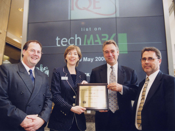
IQE joins the FTSE on 19 May 2000. Left to right are Chris Meadows, Investor Relations Manager at IQE, the CEO of the FTSE, IQE CEO Drew Nelson, and Howard Williams, Operations Director.
Illustrating this point is the re-shaping of Nelson’s former employer, BT, which made many great contributions to the development and manufacture of fibre-optic networks. “Today British Telecom imports 100 percent of its fibre-optic systems from China,” says Nelson. “And ironically, we probably build a significant amount of the InP chips that end up in those systems here in Cardiff.”
Nelson’s efforts at helping to develop a Compound Semiconductor cluster in South Wales also involved working within a group set up by the European Commissioner for Technology for the Digital Economy. Involved in a team looking at key enabling technologies, Nelson focused on how to rebuild the continent’s manufacturing capability in compound semiconductors. His solution: construct a sovereign capability for compound semiconductors in South Wales. “It seemed a very good way to provide a more competitive edge for the UK, and for Europe.”
The next step involved lobbying the Welsh Government and Cardiff University to invest in an Institute for Compound Semiconductors based at the University’s new innovation campus. Persuading them wasn’t easy, but collectively they ended up investing £75 million, which has since leveraged £17 million from the Research Partnership Investment Fund, and spurred the setting up of an EPSRC Manufacturing Hub for Compound Semiconductors, backed by £10 million.
“The vision there is to create an institute which will have capability to go up to 8-inch materials, compound semis on silicon, and to do early stage research across a broad range of materials,” explains Nelson. Some of the funding has been used to construct a new building, which could be ready as early as the end of next year. Until they move in, the researchers are working in a cleanroom that has been upgraded for 6-inch processing.
“The big difference now with the approach of the university is that they want to build the cleanrooms and use the tools with industrial discipline,” says Nelson. “So rather than just having labs that any student can come in and play with, the equipment is being run on a much more industrial-like and professional basis.”
This new approach may assist the efforts of the researchers, according to Nelson. As experiments require a change to one parameter while keeping all the others the same, the greater rigour of all the processes in the cleanroom should make it easy to identify the reason behind a change.
To take the best ideas that come out of the University and provide a pathway to commercialisation, IQE and the University have set up a joint venture, known as the Compound Semiconductor Centre (CSC). With funding from Cardiff University and some equipment from IQE, CSC, which is now in its third year, has more than ten significant collaborative research projects underway.
Another key partner in the cluster is Newport Wafer Fab. This 200 mm silicon facility passed into the hands of Infineon in 2015, when the German powerhouse bought International Rectifier. Infineon decided that it had more global fab capacity than it needed, so it would either sell or close the Newport fab by the end of 2017.
“I ended up leading a private equity buy-out for Newport Wafer Fab,” explains Nelson. “The direction of travel for that as part of the compound semi cluster is to transition from 100 percent silicon to building compound semi-on-silicon chips at 200 millimetre.” The later could include power and RF devices made from GaN-on-silicon, silicon photonics incorporating III-V devices, and structures that feature an intermediary layer of crystalline rare earth oxides.
Other key players in the cluster include: SPTS, a provider of etching and deposition equipment to the compound semiconductor industry; packaging expert Microsemi; and Swansea University, which has a large nano-health centre, and is setting up a centre for Integrative Semiconductor Materials.
Last but by no means least is the Compound Semiconductor Applications Catapult, an open access R&D facility focused on helping UK businesses exploit advances in compound semiconductor technologies.

IQE’s facilities have grown over 30 years, and now include fabs in Greensboro, North Carolina (bottom left) and Singapore (top left). In Cardiff, capacity is increasing with the a new fab being built (bottom right) that will complement the one at St Mellons (top right).
The CS Catapult is moving into a building initially constructed for LG Semicon. “The main fab is now used as what I believe is Europe’s largest data centre, and the building next to it is package-andtest, which is highly suited for fitting out as an epi facility.”
That is the plan for this building, which is being re-purposed with support from Cardiff City Region. Other cluster partners will share this with IQE, which is setting up a compound semiconductor epifoundry there. “This is going to be, we believe, the biggest in the world for outsourced epi,” says Nelson. “It has the capability of housing 100 MOVD tools.” The Catapult will be located in a separate part of the building.
Working together, those within the cluster are covering all aspects of production, from wafers to chips, package devices and equipment. “So anyone can interact with the cluster at any point they wish, whether it is for production, for R&D, or for development,” say Nelson. With such a hubbub of activity, those wishing to work with the cluster may be unsure who to approach. To address this, a brand name has been set up, CS Connect, which can provide a point of contact for all interested parties.
The impact that the cluster is having is delighting Nelson, who is clearly passionate to see more high-tech manufacturing within the UK: “We’ve even got examples of fairly significant companies in Asia outsourcing high-tech manufacturing to the Cluster. This is a complete, 180-degree turnaround for the cluster from what you would expect – UK companies outsourcing all the hi-tech manufacturing to Asia.”
Thirty years on from the launch of his epiwafer company, it is clear that Nelson is not resting on his laurels. He is as enthusiastic as ever to drive success at IQE, but now this mission extends to triumphs for the cluster.
IQE’s key milestones
1988 Launch of Epitaxial Products International (EPI)
1999 EPI merges with QED and floats on the EASDAQ
2000 IQE floats on London Stock Exchange
2000 Launches subsidiary IQE Silicon and acquires Wafer Technology in Milton Keynes, UK
2006 Acquires Emcore’s Electronic Materials Division in New Jersey, USA
2007 Acquires MBE Technologies of Singapore
2009 Acquires GaN nanotechnology expert NanoGaN of Bath, UK
2010 Acquires antimony substrate maker Galaxy Semicondcutors of Spokane, WA
2012 Acquires the epi-business of RFMD in North Carolina, USA
2018 Acquires the pioneer of crystalline rare earth oxide layers, Translucent of Palo Alto, CA
Compound semiconductor highlights at this year’s VLSI included tunnel FETs with a record-breaking subthreshold swing, GeSn transistors with a fin width below 10 nm, and InGaAs photoFETs setting a new benchmark for responsivity Richard Stevenson reports
For a decade or more, our community has devoted much effort to the development of III-V transistors for maintaining the march of Moore’s Law. It has been argued that armed with a superior mobility to silicon devices, those made from compound semiconductors can operate at a lower voltage while maintaining current, and thus enable power scaling at future nodes.
Progress of these devices is continuing, with some of the latest breakthroughs reported at the 2018 Symposium on VLSI Technology and Circuits, held in late June in Honolulu, HI. At that gathering, where there were also reports of progress associated with III-V photodetectors, highlights included talks on: tunnel FETs made from InGaAs and GaAsSb with a sub-threshold swing that broke new ground; GeSn FinFETs with a fin width below 10 nm that set a new benchmark for transconductance; and tuneable InGaAs nanomenbrane photoFETs on flexible substrates, which are promising for lightweight, wide-angle imaging applications.
Superior sub-threshold swing
Makers of these record-breaking tunnel FETs, Alireza Alian and co-workers from imec, Belgium, claim that their best devices, which sport a vertical nanowire architecture, produce a record transconductance of just 47 mV/decade. This low value is important, because it allows the device to operate at a lower power supply voltage while still delivering a high current. For imec’s leading FETs, the drive current is 700 μA/μm at 0.35 V, for a fixed off-current of 1 nA/μm. That voltage is far lower than that used in today’s ICs, which operate at around 0.9 V, highlighting the promise of III-V tunnel FETs for all mobile applications, where they could lengthen battery life.
imec’s best results were obtained with nanowires with a 30 nm diameter. For insertion in a future node they would need to be “somewhere around ten nanometres”, says Alian.
Another group in Europe, based at Lund University, have also produced encouraging results with vertical nanowire devices. “They did it using grown wires,” says Alian. “We got quite similar results by etching the wires.”
In Alian’s view, the top-down approach that he and his co-workers adopt is better suited to high-volume manufacture. “It is believed to be more controllable – and less variability is expected than when you grow the wires.”
Fabrication of imec’s tunnel FETs begins with the growth of III-V layers on an InP substrate. The researchers employ this growth process, rather than MOCVD, because they believe it produces better interfaces. “CVD is usually at a higher temperature than MBE, so intermixing at interfaces is more severe,” argues Alain.
The team produced a range of tunnel FETs, formed from nanowires with diameters of either 30 nm, 50 nm, 70 nm or 90 nm. Electron beam lithography defines their diameter, prior to etching into the heterostructure at 100 °C with a methane-based plasma to create these structures. Atomic layer deposition adds a gate oxide, comprising 1 nm-thick Al2O3 and 2 nm-thick HfO2. Fabrication finishes with the addition of a top spacer, top and back contacts, and in some cases an anneal in forming gas at 350 °C (see Figure 1 for a device architecture).
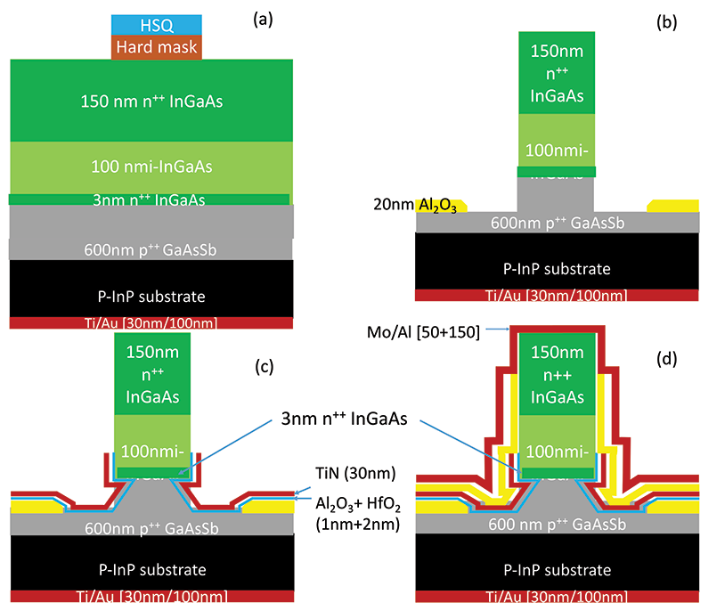
Figure 1. Formation of imec’s tunnel FET begins with the growth of a heterostructure by MBE, and the use of lithography to define the diameter of the nanowires (a). Dry etching forms the nanowires (b), before a gate stack is added by atomic layer deposition (c), and a top spacer and top and back contacts are introduced (d).
Measurements on various devices, which have been studied with several microscopy techniques (see Figure 2), reveal significant variations in the drive current and the threshold voltage for transistors with the same nanowire diameter. These variations, which could be addressed by optimising the process, are attributed to unintended differences in doping and nanowire diameter.
Alian and co-workers observed a negative differential resistance in the output characteristics of their transistors, confirming that device behaviour is dominated by tunnelling. Performance improves with annealing in the forming gas, thanks to a reduction in the density of interface traps in the InGaAs layer.
A sub-threshold voltage below 60 mV/decade is only observed in devices with a nanowire diameter of 30 nm and 50 nm. This suggests that narrower wires improve sub-threshold voltage, a conjecture backed by simulations of the band-to-band tunnelling current – they indicate that shrinking the nanowire diameter to 20 nm could decrease the subthreshold swing to 20-30 mV/decade.
Any shrinking of the diameter of the nanowires must go hand-in-hand with increases in the source doping and a reduction in gate-source overlap. “Achievinghigher doping is not difficult,” says Alian, who believes that it is easy to realise levels of 5 x 1019 cm-3. “For the overlap, it is possible, but variability is expected to become an issue.” However, this can be addressed by engineering.
Alian and co-workers are hoping to now investigate the effects of higher doping. After this, the team may go on to study devices with narrower diameters.
Very fine fins
A claim for record-breaking miniaturisation came from a partnership between the National University of Singapore, Nanyang Technological University and Applied Materials. This collaboration believes that it has broken new ground by making GeSn pFETs with a fin width below 10 nm. The width at the top of the fin, produced on a 200 nm GeSn-on-insulator substrate, is just 5 nm.
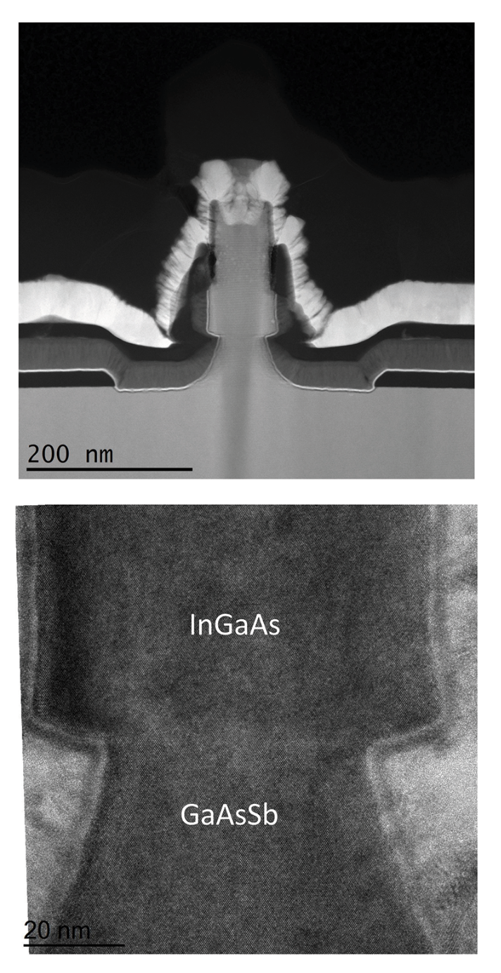
Figure 2. Scanning transmission electron microscopy of the tunnel FET produced by the team at imec (a) can reveal the high quality of the InGaAs and GaAsSb layers (b).
This is not the ultimate limit, though – team spokesman Xiao Gong from National University of Singapore believes that optimizing the sidewall angle of the GeSn fin could lead to even smaller fin widths of about 3-5 nm. “The question is, at such small fin width, how high a mobility or source injection velocity can we achieve.”
Gong says that the team’s devices, which could make an impact at the sub 3 nm node, are produced with a process that is repeatable and straightforward.
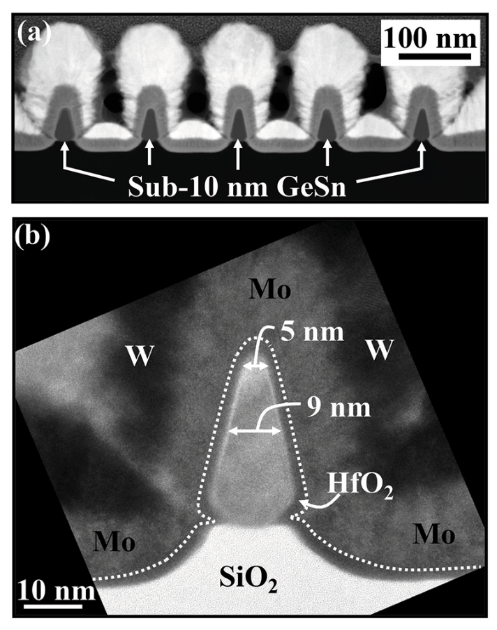
Figure 3. (a) Darkfield transmission electron microscopy images of the GeSn p-finFETs produced by the team from the National University of Singapore, Nanyang Technological University and Applied Materials. (b) A highresolution transmission electron microscopy of a GeSn fin surrounded by the high-κ dielectric and the metal gate.
“The GeSn fins were first formed using an ICP dry etch to achieve a smallest fin width of about 15 nanometres. A digital etch process was then employed to trim it down to sub-10 nanometres.”
The only step in the fabrication process that is not suitable for high-volume manufacturing is the patterning of the wafer by electron-beam lithography. But Gong says that this weakness can be overcome by turning to optical lithography.
Fabrication of the devices begins with CVD of a 10 nm-thick film of Ge0.95Sn0.05 on a silicon substrate. Using Ge0.95Sn0.05, rather than pure germanium, leads to a 55 percent hike in high-field hole mobility, according to experiment.
The next steps in device fabrication are: the definition of the channel; source and drain implantation, using boron; activation of the dopants, by heating the wafer to 400 °C for 60 s; forming the fins with a chlorinebased ICP etch, and then trimming with a digital etch; adding a gate stack, using process temperatures below 250 °C; etching the gate; and adding source and drain contacts (see Figure 3 for images of the devices).
A range of FinFETs have been produced with channel lengths from 50 nm to 200 nm, fin widths from 9 nm to 20 nm, and fin heights of 30 nm.
Measurements reveal that the smaller the fin width, the greater the suppression of short-channel effects. This helps to lower the sub-threshold swing, which fell from a minimum of 90 mV/decade for FETs with a 30 nmwide fin to a minimum of 63 mV/decade for a variant with a 9 nm-wide fin.
Other important characteristics of the transistors are a transconductance that can be as high as a record-breaking 900 μs/μm, an on-current that can hit 420 μA/μm at 1 V above threshold, a high hole mobility (see Figure 4) and an on-off ratio of 104. When judged in terms of the ratio of transconductance to saturated sub-threshold swing, the team’s best device hits 10.5, a value that is claimed to be a record.
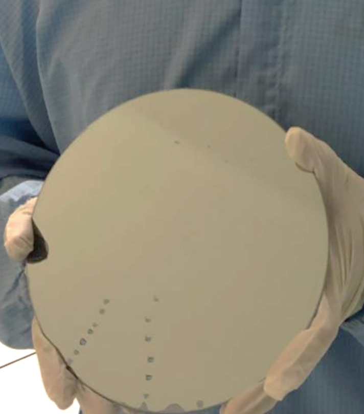
The 200 mm GeSn-on-insulator substrate used by the team from the National University of Singapore, Nanayang Technological University and Applied Materials to produce sub-10 nm pFETs with a record-breaking ratio of transconductance to saturated sub-threshold swing.
This figure-of-merit is important, according to the team, because it captures several key metrics. “Saturated sub-threshold swing gives you the information of the gate stack quality and on-off ratio for the current at a high drain-source voltage,” says Gong, while the transconductance indicates the drive current that may be realised in the on-state. “For a transistor, we would like the ratio of transconductance to saturated sub-threshold swing as high as possible.”
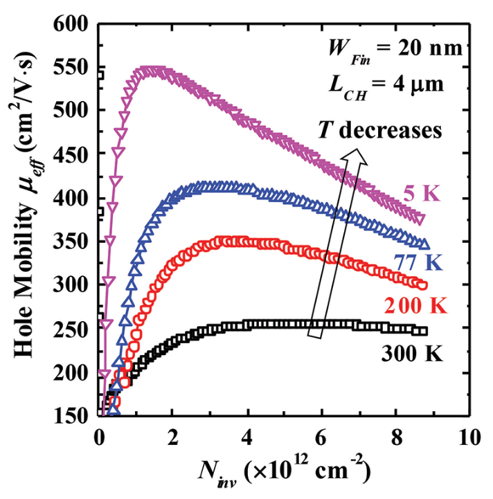
Figure 4. The effective mobility as a function of inversion carrier density, for GeSn pFETs produced by a partnership between researchers at the National University of Singapore, Nanyang Technological University and Applied Materials.
One of the next goals for the team is to replicate the good performance of the sub-10 nm GeSn p-finFETs with GeSn n-finFETs. “Gate stack and source/drain engineering for nFETs will be done to reduce the interface trap density and reduce the source/drain series resistance,” explains Gong, who reveals that the team may also investigate the use of GeSn as the channel in TFETs.
Flexible photo-transistors
Two major changes in the coming decades will be the introduction of smart vehicles and autonomous drones. Both will benefit from lightweight imagers operating in the near and short-wave infrared – and if these devices could cover large surfaces, alongside detectors, they could also aid the development of ultra-light machines with wide-field imaging capability.
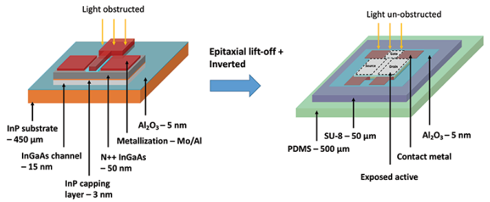
Figure 5. Researchers at imec and the National University of Singapore create a flexible, high performance device by using epitaxial lift-off to mount, on a polymer, an InGaAs-on-InP MOSHEMT with an exposed InGaAs channel.
A promising option for such detectors is being pioneered by a team from imec and the National University of Singapore. Their approach, detailed at the latest VLSI meeting, involves the use of epitaxial lift-off to expose the InGaAs channel of an InGaAs-on-InP MOSHEMT and create a flexible device that is more sensitive than existing silicon and III-V photodetectors in the near and short infrared (see Figure 5).
Spokesman for the team, Yida Li from the National University of Singapore, says that the motivation behind this is the aim of building a device that is flexible and lightweight. “This may allow us to enable imaging arrays on large-area surfaces to replace bulky hyperspectral imagers.”
Li and co-workers decided to detect the light with high-quality layers of InGaAs, which they believe offer some advantages over more popular, but less mature, two-dimensional materials, such as graphene and MoS2. “We have exploited one key advantage of thinfilm devices by lifting off and inverting the device, to increase its photosensitive area, while allowing it to be flexible,” argues Li.
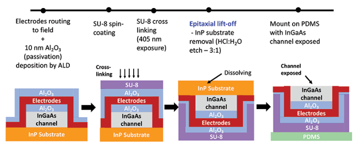
Figure 6. The photoFET is fabricated with a series of steps that include spin-coating, epitaxial lift-off and exposure of an InGaAs channel.
Fabrication of the photoFETs begins with the growth of an InGaAs MOSHEMT on an InP substrate. Following meas isolation and the routing of electrode contacts to the field area, this epiwafer is bonded to an epoxy-based negative photoresist, SU-8, before the InP substrate is removed and the InGaAs channel exposed (see Figure 6 for details)
“The SU-8 is used to protect the photo devices from the chemical etch process, as well as to serve as a flexible backing for the ELO devices,” explains Li.
He believes that these detectors could be produced with high-volume processes. “In this work, we explored the transfer of complete devices with metallization. This may allow for entire arrays of connected devices to be transferred rather than individual devices, leading to increased density and throughput.” Alternatively, production could draw on high-precision heterogeneous pick-and-place, which Li says is a base technology in advanced wafer-level packaging.
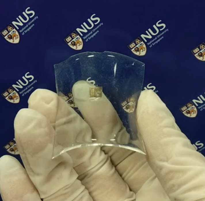
The photoFET, on a polymer substrate, shows no signs of degradation when flexed with a radius of 10 cm.
Device measurements reveal that for a gate bias range of 6 V, photocurrent can be tuned by over five orders of magnitude. The on-state photoresponsivity is 380 A/W at 660 nm, and 15 A/W at 1877 nm, values that are claimed to be more than double those for existing silicon and III-V photodetectors. No degradation in performance is observed when the device is flexed with a radius down to 10 cm.
To improve performance in the short-wave infrared, the team can adjust the composition of InGaAs. “There is nothing that stops us from lowering the bandgap with higher indium content or moving to a lower-bandgap III-V for longer wavelength sensitivity,” says Li, who points out that such a move would need to strike a balance between dark current leakage and sensitivity.
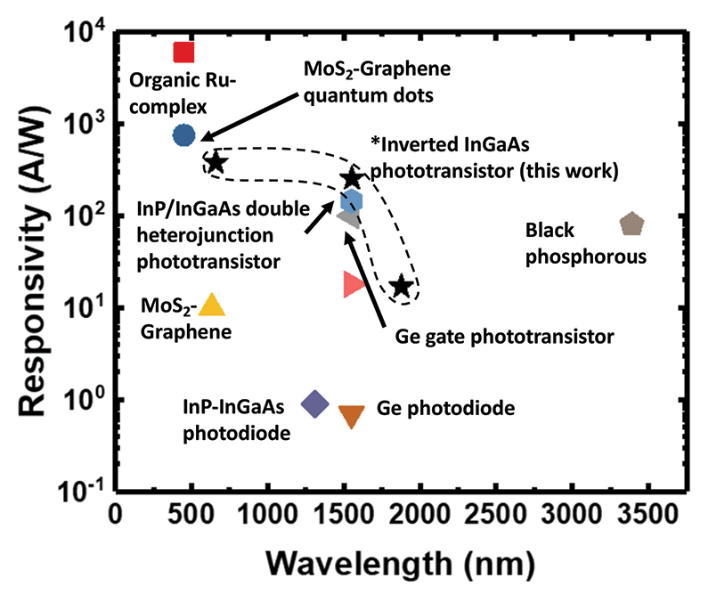
Figure 7. The responsivity of the InGaAs photoFET is far higher than that of many rival technologies.
The next goals for the team are to improve device performance through optimisation of the process, and to investigate opportunities to scale up to larger arrays.
This effort, and those that have led to record values for both the sub-threshold swing of vertical nanowire tunnel FETs and for the transconductance of GeSn pFETs with sub 10 nm fins, highlight the innovation within the compound semiconductor industry. Further breakthroughs in these areas will be reported at next year’s VLSI – and prior to that, at the next IEDM, to be held on 1-5 December in San Francisco.
GaN FETs featuring a thin unintentional doped GaN interlayer as the channel and an in-situ grown gate-dielectric can boost efficiency at the system level, thanks to a higher channel mobility and lower on-resistance. By Dong Ji and Srabanti Chowdhury from the University of California, Davis, and Chirag Gupta and Umesh Mishra from the University of California, Santa Barbara
Power converters are widely used in power electronic systems, where they convert one form of electrical energy to another. They are used to form rectifiers, which convert AC voltages to those that are DC; they create inverters that provide the DC to AC conversion; and they step up and down DC and AC voltages.
Due to the widespread use of power converters, any increase in the efficiency of power electronics can play a crucial role in reducing the global carbon footprint. Currently, two-fifths of all the energy that is consumed is first converted into electricity, and this figure may rise to three-fifths with increasing use of electric and plug-in hybrid vehicles and high-speed rail transportation. And by 2030, it is anticipated that as much as 80 percent of electrical energy will pass through power electronics between generation and consumption.
To help to increase the efficiency of power electronics, in 2014 ARPA-E launched a new programme called SWITCHES – it is short for Strategies for Wide Bandgap, Inexpensive Transistors for Controlling High-Efficiency Systems. This effort, involving five universities and nine companies, has focused on the development of 1.2 kV power transistors that have the potential to realize functional cost parity with silicon-based devices.
Our team from the University of California, Davis, and the University of California, Santa Barbara, has played its part in this programme. Our contribution has been the development of a novel device – an in-situ oxide, GaN interlayer based MOSFET – that sets a new benchmark for DC performance at 1.2 kV.
The power electronics revolution
Today silicon, in the form of the MOSFET and the IGBT, dominates the market for power semiconductor devices. However, this pair of incumbent transistors is reaching a performance plateau, and almost all improvements are incremental.
To reach a new level of performance for power switching, there needs to be an uptake in devices made from wide bandgap materials, such as GaN and SiC. Devices made from these materials are able to set a new benchmark for the trade-off between the breakdown voltage and the on-resistance (see Figure 1).
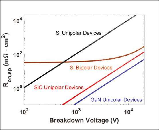
Figure 1. The tradeoff between the specific on-resistance (Ron,sp) and the breakdown voltage for silicon and it two leading challengers, SiC and GaN
For GaN, the first generation of power transistor is the HEMT. It sports a lateral geometry and takes advantage of a two-dimensional electron gas channel, introduced by the polarization of the AlGaN/GaN heterojunction. Thanks to the high electron density and high electron mobility in this channel, the GaN HEMT can combine operation at high power with an extremely low on-resistance.
Following two decades of development, the GaN HEMT has been commercialized, with devices offering blocking voltages of 650 V or less. The blocking voltage is held by depleting the lateral channel between the gate and drain electrodes. So, to realise higher blocking voltages, there has to be an increase in the gate-to-drain spacing. In addition, to achieve high output current, the device must be scaled up in width. However, as a result, the device area is then so large that it is impractical for any application requiring blocking voltages over 1 kV.
Vertical virtues
For higher voltages, a far better approach is to build a vertical device. With this architecture, the device holds the blocking voltage in the bulk of the material by depleting the drift region, and the peak electric field occurs in the bulk GaN. A merit of this approach is the elimination of surface-state related dispersion, realised without the need for any special field plating structure. Note that to scale the current and the voltage, there must be an increase in the gate width and the drift region thickness, respectively.
The vertical GaN transistor is capable of delivering a very impressive power-handling capability. It is possible for a single die to simultaneously realise blocking voltages in excess of 1 kV and currents of more than 100 A. Such a high level of performance makes the vertical GaN transistor a more economical and viable solution for high-voltage and high-current applications.
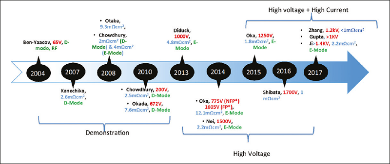
Figure 2. The development of vertical GaN FETs.
The development of vertical GaN transistors can be traced back to the launch of single-crystal GaN substrates. Following a few quiet years, vertical device research took off in 2007 (see Figure 2). Milestones include Avogy’s development of a vertical JFET, which offered paths towards commercialization. Trailblazing efforts from that era have helped to spur wider support for vertical GaN transistors, and encourage further development of this device.
Our contribution to this field is a modification to the design of the vertical GaN transistor that improves channel properties. In a conventional GaN trench MOSFET, the channel forms on the vertical etched p-GaN sidewall, where sidewall roughness, ionized impurity scattering and ex-situ gate-dielectric deposition can hamper the performance of the channel. We address these weaknesses by using MOCVD to grow, on the trench structure, a thin unintentionally doped GaN interlayer, followed by an in-situ dielectric (see Figure 3 and Table 1).
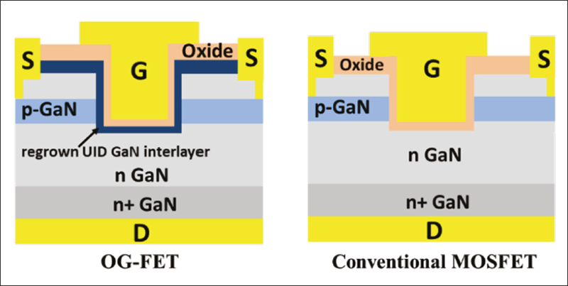
Figure 3. Cross-section profiles of the in-situ oxide, GaN interlayer based MOSFET and the conventional MOSFET.
These refinements improve performance. The thin GaN interlayer increases channel conductivity with normally-off behaviour. In turn, there is a higher channel conductivity, alongside an improved channel/oxide interface that results from our in-situ regrowth technology, and this leads to a lower and better dynamic on-resistance. Thanks to these improvements, there is an overall reduction in switching energy losses and a hike in device reliability. In addition, this form of FET is free from current collapse, which is caused by the surface states.
Improvements in performance have been revealed by measurements made on our in-situ oxide, GaN interlayer based MOSFETs. When providing normally-off behaviour, realised by using a threshold voltage of about 2 V, they offer the same breakdown voltage as trench MOSFETs.
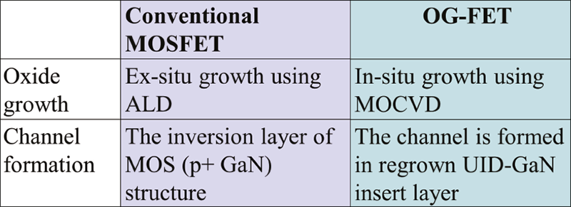
Table 1. Comparison of the conventional MOSFET and the proposed in-situ oxide, GaN-interlayerbased MOSFET.
Adjustments to our device can increase its blocking voltage. Without edge termination, our in-situ oxide, GaN-interlayer-based MOSFET is capable of a breakdown voltage of between 700-1000 V and onresistances of just 2.5-3 mΩ cm2 – this is for normallyoff operation, realised by applying threshold voltages in the range of 1-3 V. Adding a field plate enhances off-state performance beyond 1 kV, and turning to a double field plated structure propels the breakdown voltage to 1.4 kV (for a threshold voltage of 4.7 V and an on-resistance of 2.2 mΩ cm2).
There is a hysteresis is associated with the in-situ channel interface and the oxide. When Al2O3 is used, the threshold voltage can shift by about 0.3 V. To reduce this, we have turned to AlSiO, a move that has slashed the threshold voltage shift to below 0.1 V and improved DC performance.
So that we can demonstrate the performance advantage provided by our device at the system level, we have developed a device-circuit hybrid model. This enables a comparison of a power electronics system that uses the GaN FET as the switch with variants that use silicon and SiC. Our effort is both important and worthwhile, as there are no commercial pieces of software for modelling GaN devices and evaluating switching characteristics.
With our hybrid model, one can start by simulating the device with a two-dimensional drift-diffusion model, and go on to study its characteristics in a circuit, where an evaluation of its switching performance is possible. This approach offers an inexpensive, accurate way to project and benchmark performance. Note that it can be extended to any GaN-based power transistor (see Figure 4 for a flowchart of the hybrid simulation developed at UC Davis).
Using this model, we found that our GaN FETs have more than 30 percent lower switching losses than conventional trench MOSFETs, enabling the system to be operated in megahertz range with over 90 percent efficiency.
We will now build on our success with 1.2 kV GaN FETs that deliver excellent DC performance. Our next step will be to use these devices to investigate switching and reliability behaviours.
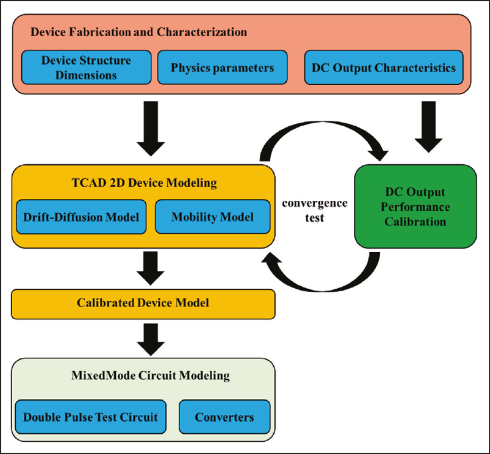
Figure 4. Flow chart of the device-circuit hybrid model.
Further reading:
Patterned silicon provides a promising foundation for non-polar and semi-polar GaN LEDs that could sport unprecedented modulation speeds and bright emission in the green and yellow by Kai Ding, Natalia Izyumskaya, Ümit Özgür, Hadis Morkoç and Vitaliy Avrutin from Virginia Commonwealth University and Sebastian Metzner, Frank Bertram and Jürgen Christen from the Otto-Von-Guericke University
Of the billions of GaN LEDs made every year, the vast majority are produced by growing epilayers of nitrides on c-plane sapphire. It is an approach that’s now relatively easy to take, but the LEDs that result suffer from two fundamental flaws: a reduced overlap of the electron and hole wavefunctions, due to a strong polarization field in the active region; and a low efficiency for the incorporation of indium in the InGaN quantum wells. Both these issues contribute to the ‘green-gap’, a low efficiency for LEDs emitting in the green and yellow; and they hamper the development of full colour displays, laser diodes, and highbrightness sources for general lighting.
What’s more, the strong polarization fields in the active region – a phenomenon that goes by the name of the quantum confined Stark effect – imposes serious limitations on Li-Fi, an emerging communication technology that uses light to transmit data over free space. Spatial separation of electron and hole wave functions that results from these fields leads to long carrier lifetimes: for blue LEDs it is tens of nanoseconds, and for green variants it is an order of magnitude higher. The lengthy lifetimes limit LED bandwidth to the megahertz range.
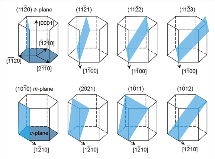
Figure 1. Select low-index crystallographic planes in group-III nitrides.
One promising approach to enhancing the modulation speed of the LEDs, and also increasing their efficiency in the green and yellow, is to switch growth from the polar orientation to one that is either semi-polar or non-polar. The former reduces the polarization fields, while the latter eliminates them completely (see Figure 1 for common non-polar and semi-polar planes).
For semi-polar planes, the angle made with the polar c-plane governs the extent that the electric field is reduced. When devices are made on semipolar (1101) and (1122), thanks to inclinations close to 60° with respect to the c-plane, the polarization discontinuity at InGaN/GaN interfaces is sufficiently small, aiding the fabrication of green devices with tolerable compositions of InGaN. Note that in theory, the weakening of the fields, which push emission to shorter wavelengths, is not the only benefit of semi-polar planes – they also promise to enhance the efficiency of indium incorporation.
What platform?
The ideal platforms for non-polar and semi-polar LEDs are native substrates with identical orientations. But natural limitations are making such structures prohibitively expensive for mass production. Today, HVPE and ammonothermal methods can produce relatively large GaN crystals, but these approaches are hindered by the strong tendency of GaN to grow in the polar (0001) direction. With HVPE it’s possible to produce (0001)-oriented disks that are a few millimetres thick, limited by large internal stress; while the ammonothermal method yields hexagonal prisms that are a few centimetres thick, with a (0001) base plane (see Figure 2). In this case, crystal thickness is limited by the low growth rate. Due to these limitations, the non-polar and semi-polar substrates that are diced from (0001)-oriented boules are elongated rectangles with a width of no more than a few centimetres.
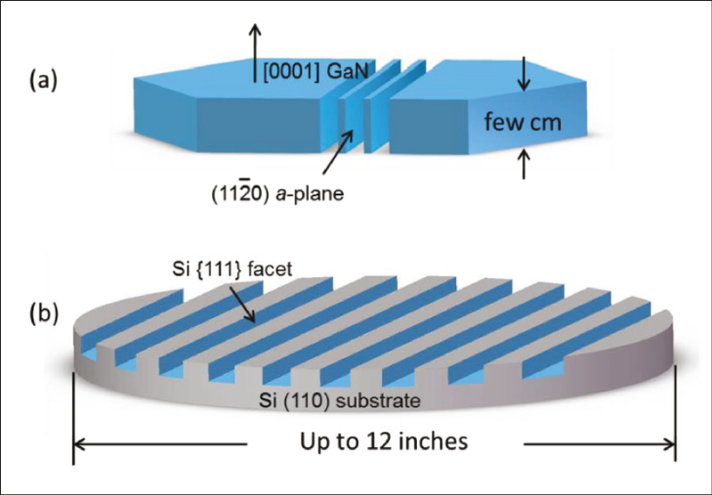
Figure 2. Comparison of the available GaN and silicon substrate sizes for growth of non-polar and semi-polar GaN (taking non-polar (1120) GaN as an example): (a) ammonothermal GaN, and (b) patterned silicon (110) substrate.
One promising alternative, which we are pursuing at Virginia Commonwealth University, VA, and the Otto-von-Guericke University in Germany, is to grow semi-polar and non-polar LEDs on patterned silicon. This approach has much to recommend, as silicon substrates are low in cost, available in large sizes, and allow the use of processes that are compatible with mature silicon technology. For example, a silicon platform could allow the combination of drive circuitry and LEDs on a single platform.
Many groups, both in academia and industry, have developed c-plane LEDs on silicon. A great deal of their efforts have focused on the development of stress compensating buffer layers, which mitigate a large tensile strain induced by the large thermal mismatch between silicon and GaN. Left unchecked, this strain causes the material to crack.
Unfortunately, none of the orientations of silicon can be directly employed to grow non-polar or semi-polar GaN LEDs. However, due to its epitaxial relationship with GaN, patterned silicon can provide a platform for growing GaN with various non-polar and semi-polar planes.
The key to producing non-polar and semi-polar orientations is the exposure of the {111} facets of a properly oriented silicon substrate for GaN nucleation (see Figure 3). As GaN grows epitaxially on silicon (111) in the c-direction, thanks to the epitaxial relationships GaN <0001>||silicon <111> and GaN <2110>||silicon <011>, it is possible to form: nonpolar (1100) (m-plane) and (1120) (a-plane) GaN on patterned silicon (112) and silicon (110) substrates, respectively; and semi-polar (1101), (1122), and (2021) GaN on patterned silicon substrates of different orientations.
We have undertaken experimental studies that confirm the theoretical predictions for complete elimination of the polarization field at the interfaces in nonpolar InGaN/GaN and GaN/AlGaN heterostructures, along with the substantial reduction in the semipolar varieties. Our photoluminescence spectra from (1100)-oriented 6 nm InGaN/GaN double heterostructures show no blue-shift with increasing excitation, suggesting an absence of the polarization fields and thus the elimination of the quantumconfined Stark effect. For semi-polar (1101) 6 nm In0.15Ga0.85N/GaN double heterostructures emitting in the blue, the shift to shorter wavelengths is just one-fifth of that for c-plane counterparts (see Figure 4). Note that similar results have been reported for other semi-polar orientations.
Recent experiments indicate that the benefits of the weaker fields are not limited to shorter radiative carrier recombination lifetimes, but extend to the dominance of radiative recombination by excitons – this is particularly attractive for high-efficiency LEDs and lasers. We have shown this to be the case in non-polar and semi-polar GaN/AlGaN systems, while teams at Cambridge and the University of Brunswick – Institute of Technology have identified this behaviour in InGaN/GaN heterostructures.
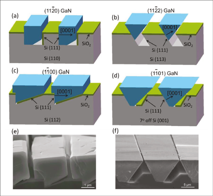
Figure 3. The growth geometry for non-polar (1120) (a) and (1100) (c) and semi-polar (1122) (b) and (1101) (d) and scanning electron microscope images for non-polar (1100) (e) and semi-polar (1101) (f) GaN on patterned silicon substrates.
The impact of piezoelectric fields on carrier lifetime is significant. Our efforts have revealed that switching from non-polar (1100) GaN/AlGaN to semi-polar (1101) lengthens the carrier lifetime from 100–160 ps to 355 ps. Meanwhile, measurements at the University of Brunswick – Institute of Technology have shown that radiative recombination lifetimes in blue-emitting InGaN/GaN quantum wells formed on non-polar m- and a-planes and semi-polar (1122) and (2021) planes have radiative recombination lifetimes from 100 ps to 1 ns. These lifetimes are far shorter than those in c-plane quantum wells, and there is also a substantial reduction in non-radiative recombination.
However, when the indium content in the wells is high, semi-polar LEDs can be dogged by lengthy radiative recombination times. Measurements by a team at the University of California, Santa Barbara, have shown that in In0.36Ga0.64N/GaN quantum wells the radiative lifetime is 30 ns. This is attributed to the spatial separation of electrons and holes, due to an in-plane component of the electric field that arises from faceting of the growth front at the nanoscale.
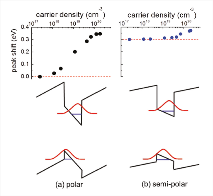
Figure 4. Photoluminescence peak position, plotted as a function of photoexcited carrier density (excitation wavelength 380 nm) for polar (c-plane) and semi-polar (1101) plane 6 nm InGaN/GaN double heterostructures on c-sapphire and patterned silicon (001). The dashed lines indicate energy levels corresponding to energy diagrams shown.
So semi-polar and non-polar planes do not guarantee short radiative recombination lifetimes, and it is therefore imperative to understand the associated growth dynamics and fundamental limitations of the III-nitride material system in this context.
One of the merits of MOCVD growth of GaN on patterned silicon is that it can eliminate extended defects. Thanks to this, a team from Nagoya University, Japan, has been able to realise dislocation densities as low as 1×105 cm–2 in semi-polar (1122) GaN stripes by employing two-step selective growth on patterned silicon (113) substrates.
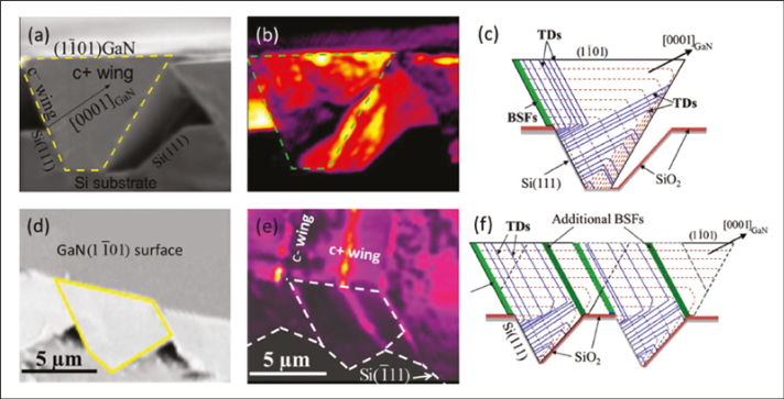
Figure 5. Comparison of defect distribution in (101) GaN grown on silicon (001) substrates with (a-c) wide-groove and (d-f) narrowgroove patterns: (a) and (d) scanning electron microscope images and (b) and (e) 10K cathodoluminescence images. Dark regions on cathodoluminescence images have high threading dislocation densities and bright regions dominate by near-band edge luminescence and/or emission from basal stacking faults. (c) and (f) GaN growth from silicon (111) sidewalls leads to threading dislocation propagation (solid blue lines) and growth front evolution (dashed lines). Note that the bottom GaN facet is in contact with the substrate surface.
We are following a similar path, investigating the growth of non-polar (1100) GaN on patterned silicon (112) substrates. With this approach, after GaN grows through the AlN buffer, it advances laterally along the GaN [0001] c+ direction – that is, the c+ wing. However, once GaN reaches the substrate surface, there is additional growth along the [0001] c− direction (c- wing) (see Figure 5). With this growth process, a fully coalesced surface is created with clear atomic steps.
Examination of this material reveals that dislocations are only generated near the GaN/silicon (111) sidewall interface, where the growth is initiated. There is a high density of basal stacking faults in c− wing regions, but the c+ wings are virtually free of extended defects.
Optimising the growth
During our efforts at developing non-polar GaN, we have found that the flow rate of NH3 can govern the characteristics of the GaN crystal. When growing non-polar (1100) GaN on patterned silicon (112) substrates, it is challenging to produce smooth m-plane surfaces with V/III ratios in excess of 700. That’s due to the appearance of stable {1101} facets. To address this, we dropped the V/III ratio to about 100. A flat m-plane GaN surface resulted, thanks to the formation of top m-facets parallel to the substrate surface and the disappearance of {1101} facets at the meeting fronts.
A low V/III ratio is not ideal, because it is detrimental to the optical properties of GaN. So our solution has been to adopt a two-step approach: we start with a low-pressure (30 Torr) stage to ensure formation of the m-plane facets; and follow this with a high-pressure step (200 Torr), designed to improve optical quality. Room-temperature photoluminescence indicates that this two-step approach is successful. Emission intensity increases by a factor of three, and deep emission is suppressed considerably.
We have also investigated the spatial distribution of extended defects in our semi-polar (1101) GaN on patterned silicon (001) substrates. A key difference between this plane and the non-polar (1100) plane is that it is stable under a wide range of growth conditions. They include high V/III ratios and high reactor pressures, both of which are favourable for producing material with a high optical quality.
Similar to the growth of non-polar (1100) GaN on patterned silicon (112), the growth of semi-polar (1101) GaN on silicon (001) commences laterally along the c+ wing. The defective c− wing is far narrower than the c+ wing, due to the far lower growth rate in the [0001] direction and the limited supply of reagents during MOCVD growth.
When we use wide groove patterns – that is, those with a width of 10 μm or more – it prevents contact between the c+ wings of GaN and the opposing silicon (111) groove wall, and the threading dislocations propagate first along the c+ direction. However, as the growth proceeds, dislocations propagating in the vicinity of {1101} growth fronts bend under the action of image forces and then propagate in the basal plane, perpendicular to the [0001] growth direction. This causes many dislocations to terminate at the upper and the lower {1101} facets (see Figure 5).
For narrower grooves, such as those with a width of 3 μm, the c+ wings of GaN come in contact with the SiO2 masking layer on the opposite wall. This leads to the formation of basal stacking faults in both the c- and c+ wings. These faults may result from a combination of a concentration of strain near the contact region; and out-diffusion of oxygen and/or silicon from SiO2, followed by surface migration of the species.
In the narrow groove structures, some of the threading dislocations that propagate initially along the c+ direction are bent onto the basal plane with further growth, while those continuing along the c+ direction are terminated when they encounter an additional basal stacking fault row. The detailed mechanism for the interaction between the threading dislocations and the basal stacking faults requires further investigation, but we can cautiously speculate that there is a bending of the dislocations at the additional basal stacking fault row interface, which is in fact a boundary between the hexagonal and cubic phase materials. At this boundary, threading dislocations turn into misfit dislocations, which extend towards the top and bottom {1101} facets. This blocking of the threading dislocations by the basal stacking fault is highly beneficial, because it leads to regions that are virtually free from threading dislocations.
The regions of high optical quality that exist between the two basal stacking fault rows are clearly evident in near-field scanning optical microscopy images (see Figure 6). This technique suggests that the overall optical quality of semi-polar (1101) LEDs on patterned silicon (001) is comparable to that of highly optimized c-polar LEDs.
The challenges
Efforts associated with the growth of non-polar and semi-polar GaN on silicon have undoubtedly produced success. However, challenges remain, related to stress management, indium incorporation and the fabrication of devices.
Managing the stress in the structure is essential. Mirroring c-oriented GaN on planar silicon (111), there is a large tensile strain, which causes cracks to form in non-polar and semi-polar GaN epilayers on patterned silicon. One option for eliminating the cracks, which has already been pursued for GaN growth on planar silicon, is to employ either stress-compensating multilayer AlN/GaN buffer layers, AlGaN buffers with a stepor linearly graded aluminium composition, or AlGaN/GaN superlattices. An alternative is to undertake selected-area growth, using epitaxial structures with lateral sizes that are smaller than the separation between the cracks. Go down this route and light emitters can be no larger than the order of 100 μm – but that is sufficiently large for microLEDs.
Theoretically, switching from the c-plane to a semipolar plane should enhance indium incorporation. However, it is not clear if this really is the case. While some groups have reported that semi-polar (1122) and (2021) planes result in higher indium incorporation than the c-plane, others are claiming that the opposite is true. It is possible that these discrepancies are due to divergence in strain relaxation in the samples studied and/or indium clustering.
So far, there are not many reports of non-polar and semi-polar GaN LEDs. And those that exist tend to focus on either the elimination or the substantial reduction of the polarization field in the active regions. What is clearly missing is a detailed comparison of this class of device with industrial-grade, state-of-the-art c-polar LEDs.
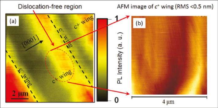
Figure 6. Room temperature near-band edge emission measured by a near-field scanning optical microscope (a) and an atomic force microsopy image (b) of the narrow-groove pattern (1101) GaN sample.
Of the non-polar and semi-polar GaN LEDs that have been demonstrated, the majority are formed on the (1101) orientation. For example, a team at Aachen University, Germany, has produced a range of semi-polar (1101) InGaN-based LEDs on V-grooved patterned silicon (001) substrates. Those that emit in the blue produce a polarization-related wavelength shift of just 4.7 nm over a current density range from 5 A cm-2 to 100 A cm-2. However, green cousins have a blue-shift of around 100 nm, attributed to indium clustering in wells with an indium content of more than 30 percent.
One promising result from the team at Nagoya University is the fabrication of a blue InGaN/GaN laser structure, formed on un-coalesced (1101) GaN microstripes on silicon (001) substrate. This structure can produce an internal quantum efficiency exceeding 90 percent at high excitation levels. Such a high efficiency is attributed to the low dislocation density that is provided by the growth geometry.
The state of play
Our work has demonstrated that like epitaxial layer overgrowth, the merits of GaN growth on pattern silicon include a trimming of the density of extended defects, both dislocations and stacking faults. So far, much of our effort has been directed at studying the mechanisms governing defect generation and propagation in these structures. This has led to several interesting findings, including dislocation blocking with rows of stacking faults, and demonstrations of material with dislocation densities that are comparable to, or even lower than, those in the state-of-the-art c-polar structures – the benchmark is dislocation densities of the order of 108 cm-2.
What is encouraging is that when the structural quality of our active regions is sufficiently high, it could enable the fabrication of non-polar InGaN/GaN LEDs that are free from the perils of the quantum-confined Stark effect. And for semi-polar variants, this affliction is far less damaging than it is for conventional cousins, so devices have the potential to combine a high brightness with a short radiative recombination time.
Of all the different non-polar and semi-polar flavours of GaN on patterned silicon, it is the (1101)-oriented GaN on silicon (001) exhibits the best structural quality to date. Encouragingly, there are also reports of a higher indium incorporation efficiency on this plane. However, more data is needed to confirm this, and fulfilling the promise will also require the demonstrate of efficient green and yellow LEDs. And even if that happens, the ultimate success of this technology will lie in the hands of the LED industry, which may or may not explore this technology for general lighting.
To date, the pace of industrial LED development suggests that there is still more to come from c-plane LEDs. If that’s the case, non-polar and semi-polar light emitters on patterned silicon will only serve niche applications. They include LiFi, which could grow considerably, and silicon photonics.
Further reading:
X. Ni et al. Appl. Phys. Lett. 95 111102 (2009)
T. Murase et al. Jpn. J. Appl. Phys. 50 01AD04 (2011)
T. Murase et al. Phys. Stat. Sol. C 8, 2160 (2011)
N. Izyumskaya et al. Proc. of SPIE 7939 79391W (2011)
S. Okur et al. Appl. Phys. Lett. 103 211908 (2013)
N. Izyumskaya et al. Proc. of SPIE 8986 898628 (2014)
B. Reuters et al. J. Phys. D: Appl. Phys. 48 485103 (2015)
R. Ivanov et al. Appl. Phys. Lett. 107 211109 (2015)
T. J. Badcock et al. Appl. Phys. Lett. 109 151110 (2016)
T. Langer et al. Phys. Stat. Sol. B 253 133 (2016)
Chip designs that exploit extreme triple asymmetry equip diode lasers with both efficiency and power by Paul Crump from FBH Berlin
In advanced industrial laser systems, which have uses that include the cutting of metals, highpower diode lasers are the source of all optical energy. In these systems, a highly intense beam is formed by either combining the optical output of many diode lasers, or by using many of them to pump a solid state or fibre laser.
Diode lasers are widely used for this task, because they are the most efficient technology for converting electrical input energy into application-ready light. However, given their key role in industrial laser systems, even higher efficiencies are preferred, along with an increase in the maximum output power. Succeeding on both these fronts requires a good understanding of the physical effects that limit performance, because this can help to guide the development of ever more sophisticated and higher performing device designs. Such efforts should focus on high-power diode lasers that are grown on GaAs substrates and emit in the 900 nm to 980 nm wavelength range, because these are the highest performing devices, and the ones in greatest demand from industry.
At the FBH Berlin, our team has devoted many years to realising a greater understanding of this class of laser, and increasing its performance. GaAs diode lasers are a very mature, highly commercially successful technology. In spite of this, there is still much to learn and substantial improvements are still possible.
Recently, we introduced sophisticated epitaxial layer structures that have increased the power and efficiency of this infra-red source. These groundbreaking devices employ extreme triple asymmetrical designs that precisely manipulate the optical field within the chip.
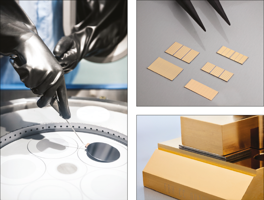
Figure 1. Left: Modern epitaxial growth tools enable sophisticated extreme triple epitaxial structures to be precisely and reproducibly grown on GaAs wafers, as needed to deliver ever higher powers and efficiencies. (Image © Maria Vittoria Trovato). Top right: Epitaxy wafers are fabricated into high-power laser bars, with geometry tailored to the application, shown here ready to be packaged for pumping or direct applications (Image © FBH/Schurian.com). Bottom right: Highpower laser bars mounted in a passively cooled heatsink, suitable for use in kilowatt-class pumping applications, where the highest power and efficiency are needed (Image © FBH/Schurian.com).
Our design is a modification of a conventional highpower GaAs diode laser (see Figure 1), which is typically grown by MOCVD. Dimensions of a standard large-area chip are a 4 mm and 6 mm length and an emission aperture of about 90 μm to 100 μm. Fabrication uses advanced III-V process techniques, such as facet passivation, while overheating is prevented by soldering the chips to a well-cooled highly conductive heatsink. High optical output is not necessarily an impediment to high reliability, and the output of the best chips is limited by fundamental loss mechanisms, rather than process or growth-related defects.
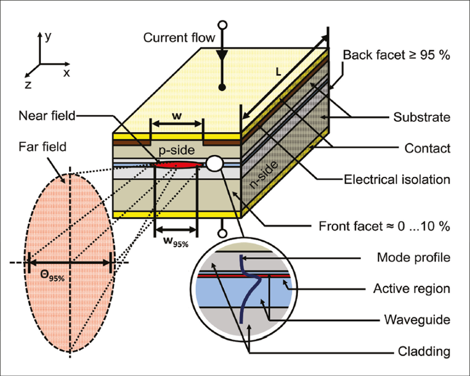
Figure 2. Conventional high-power diode laser
In all diode lasers, applying an external bias voltage drives electrons and holes towards a quantum well that is 5 – 10 nm thick. Here they are captured, and recombine to generate and amplify light. In conventional laser designs the well is surrounded by a thick, low-doped waveguide layer, itself sandwiched between two cladding layers with a lower refractive index. This architecture ensures that the optical field is confined in a region close to the quantum well (see Figures 2 and 3).
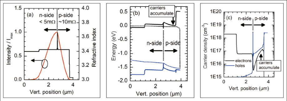
Figure 3. A conventional diode laser design has many inherent limits. (a) Vertical refractive index profile and optical field profile. More than 90 percent of the electrical resistance is from the p-side. When driven at high bias (here, 40 A in a laser with a 200 μm stripe and a 4 mm resonator), the p-side waveguide deforms, and many electrons escape and accumulate, dramatically increasing losses. This is seen in (b) the simulated vertical band structure and (c) carrier density. For more details see K.-H. Hasler et al. Semicond. Sci. Technol. 32 045004 (2017)
One of the weaknesses of these conventional highpower diode laser structures is the large difference in properties of n-type and p-type material, which supply the electrons and the holes, respectively. Specifically, the p-type material has a resistance that is ten to twenty times higher than the n-type, and an absorption that is four times higher. That is, the materials are highly asymmetric in their properties, but the vertical designs are not. Due to these imbalances, even well-optimized symmetric layer designs suffer from either high optical losses or high electrical resistance. Making matters worse, when devices are driven at high currents, a large voltage is needed to flow current through the resistive p-side waveguide. This directly limits the peak achievable power: the high voltage drop leads to band-bending, and this allows many electrons to escape from the well. When they exit, they accumulate in the p-waveguide, where they are rapidly lost. This contributes to optical losses, and limits the power produced by the chip.
Asymmetry, asymmetry...
As a first step to addressing these losses, we introduced the extreme-double-asymmetric epitaxial layer design (see Figure 4). It features two strong vertical asymmetries. The first is a thin p-waveguide – making it as thin as possible slashes the optical loss and electrical resistance. The second is a very different composition for the cladding layers either side of the waveguide, a modification that couples unwanted optical modes into the substrate. An additional merit of this design is that the thin p-waveguide prevents electron escape at high bias. Armed with this architecture, lasers have lower loss and resistance, and produce higher output powers (see Figure 4).
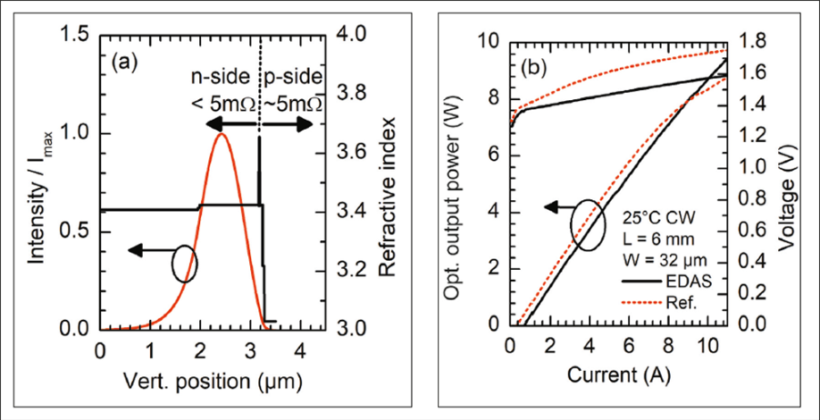
Figure 4. Extreme-double asymmetric (EDAS) structures improve performance, but problems remain. (a) Vertical refractive index profile and optical field profile. Electrical resistance from the (very thin) p-side is strongly reduced. (b) Electrical resistance is low, power saturation is improved, shown here for EDAS and conventional devices lasing close to 940 nm, with narrow stripes (32 μm) and long resonators (6 mm).
However, although performance was improved, our patented design needed further development. This double-asymmetric approach produces an offset between the optical field and the quantum well, lowering gain and leading to an increase in threshold current and a lowering of peak conversion efficiency. In addition, in spite of suppressing key power saturation effects by design, diode lasers using double asymmetry deliver significantly lower powers than predicted, even when studied using the best calibrated and most detailed simulation tools.
...and more asymmetry
To address all these weaknesses, we have recently introduced a third degree of asymmetry: an asymmetric refractive index profile for the layers either side of the quantum wells (see Figure 5). Thanks to this modification, the profile of the optical field can be finely tailored. Shifting the optical field towards the quantum well increases optical gain without the need to adjust the p-side, which can remain thin. The upshot is that, for the first time, it is possible to simultaneously realise low resistance, low loss, low power saturation and a low threshold current (see Figure 6).
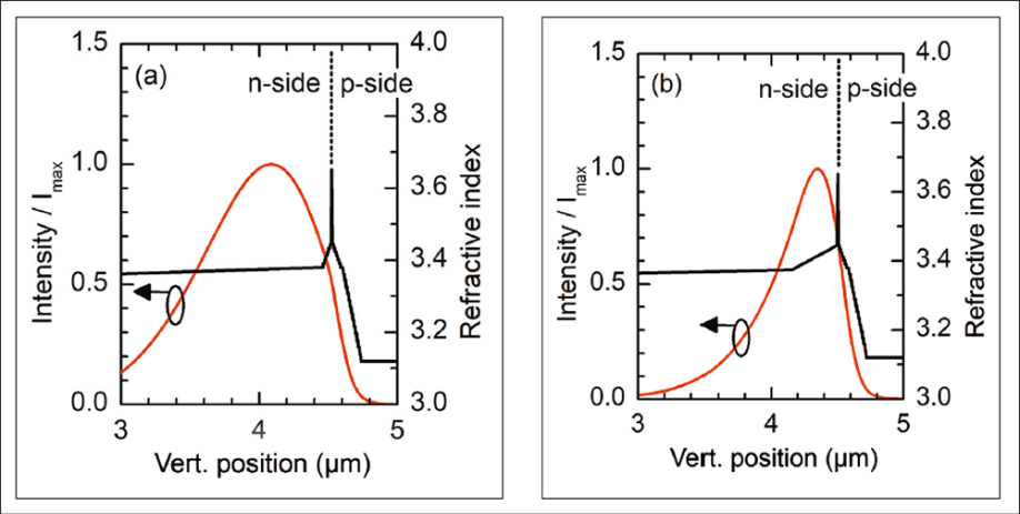
Figure 5. Extreme-tripleasymmetric structures (ETAS) further improve performance. (a) Vertical refractive index profile and optical field profile of a reference EDAS design. Gain is low, as the optical field has only small overlap with the quantum well. (b) Vertical refractive index profile and optical field profile of a new ETAS design: further asymmetry around the quantum well increases gain, without need to compromise elsewhere.
The complexity of our design, and the need for many finely tuned variations in material composition, does not imply that our laser is destined to remain in the lab. Using modern MOCVD tools and best scientific and engineering practise, fabs can reliably and reproducibly produce lasers with our design. It helps that they are constructed with the long-established GaAs-AlxGa1-xAs material system.
Our flexible mode-shaping technology, for which we have applied for a patent, is capable of producing further performance benefits (illustrated in Figure 6). Fine-tuning the vertical profile of the extreme-tripleasymmetric epitaxial structure allows the amount of light in the quantum well to be selected. It can be quantified using the optical confinement factor. When this increases, the threshold current falls and modal gain increases, leading to much lower temperature sensitivity. This attribute is highly valued in applications such as metal cutting, where the laser must operate at high temperatures in CW mode. The higher optical confinement factor obtained in devices using an extreme-triple-asymmetric epitaxial design also allows these devices to deliver higher optical powers in pulsed mode, as needed for applications like LiDAR. We are currently using both of these benefits of a higher optical confinement factor to realise higher-performance diode lasers. One of our findings may raise a few eyebrows, given that diode laser designs with high optical confinement factors are typically expected to show lower optical powers in pulsed mode, not higher.
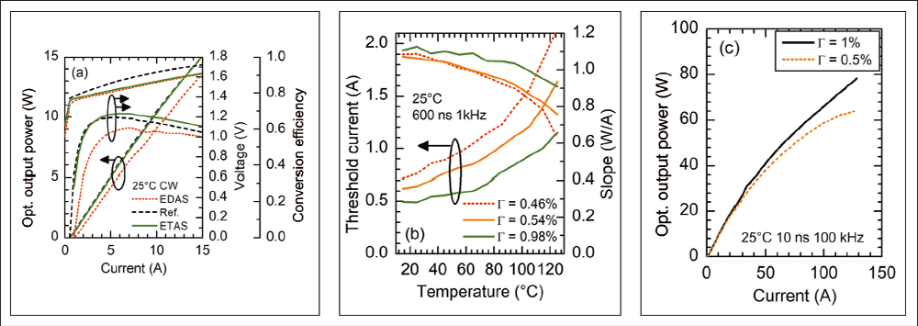
Figure 6. Experimentally demonstrated performance benefit of extreme-triple-asymmetric structure (ETAS) lasers. (a) Optical power, voltage and efficiency tested CW at 25°C for chips lasing at 940 nm with a 4 mm resonator and a stripe width around 90 μm. ETAS designs with an optical confinement factor of around 0.5 percent have the same threshold and power as conventional lasers and the same voltage as EDAS lasers, increasing peak efficiency (here to 69 percent) and efficiency at high power (here to 66 percent at 10 W). Prototype ETAS lasers with higher optical-confinement factors also show higher performance, with (b) lower temperature sensitivity (threshold and slope vary more slowly by a factor of about two) and (c) higher pulsed output powers.
The expectation is that high confinement leads to extra absorption at high bias, due to non-linear processes such as gain compression and twophoton-absorption. But our experiments show that for our designs, a high optical confinement factor and a low threshold current enable an increase in power. Or, to put it another way, the benefit of low threshold current – and hence a lower carrier density in the quantum well – more than compensates for any additional non-linear losses.
It is clear that our advanced extreme-triple-asymmetric epitaxial layer structures can set a new benchmark for the optical power and conversion efficiency of highpower diode lasers. Our technology allows the optical field to be finely tuned, enabling a low threshold to be combined with a low resistance, low loss and low power saturation. Our design is still at an early stage, and we expect that refinements to the laser and a better understanding of the power saturation mechanisms will spur performance to a new level.
The development of the extreme-triple-asymmetric epitaxial layer structure concept builds on many years of research by the FBH team, supported by close collaboration with partners in industry (including Trumpf and Jenoptik) and many public research grants (including support from the German Federal Ministry of Education and Research, BMBF, the German Research Foundation, DFG, and the EU commission).
Further reading:
T. Kaul et al. Proc. SPIE 10514 105140A (2018)
T. Kaul et al. Semicond. Sci. Technol. 33 035005 (2018)
Reducing the Schottky barrier height and improving the gate oxide will prepare the way for the production of the vertical nanowire MOSFET by Siva Ramesh from IMEC
Semiconductor Physics made great strides in the twentieth century. Studies of this form of material in the early 1900s led to an understanding of its basic properties, along with techniques on how to dope it. Further progress came in 1947, when a team at Bell Labs produced the first point contact transistor, and three key milestones followed in the 1950s: the first single crystal germanium in 1952; the first single crystal silicon in 1954; and then, in 1958, the first IC, thanks to efforts at Texas Instruments.
Rapid improvements in the IC followed, spawning the creation of the silicon industry. And in 1965, Gordon Moore quantified the rapid rate of progress: according to his prediction, now known as ‘Moore’s Law’, the transistor density on a chip would double every 18 months. This is accomplished by scaling the dimensions of the transistor, a move that must go hand-in-hand with improvements in the performance of the device. To help engineers adhere to this, in 1974 Robert Dennard and co-workers at IBM proposed a set of rules for transistor scaling.
Keeping pace with Moore’s Law, while following the guidelines of Dennard, has led to a period of extensive scaling. Performance and power specifications have been fulfilled at every new node, allowing the cost per chip to plummet. The enabler behind all this progress has been the innovation in process integration (see Figure 1).
Up until about a decade ago, advances in lithography held the key to performance improvement. But in recent times, there have been issues that can’t be addressed by just lithography, so other innovations have had to drive progress.
One of the big changes to the transistor has been the replacement of the SiO2 dielectric with HfO2. Driving this change is that the shrinking of the MOSFET leads to an increase in gate leakage current, due to direct tunnelling, so to combat this, Intel introduced HfO2/metal gates in its 45 nm technologies that were introduced in 2007.
Another recent challenge has been maintaining a reduction in power density. For many years, decreasing the applied voltage did the trick. However, that is no longer an option for silicon, with reductions in voltage compromising on-state performance. To address this, chipmakers introduced multi-core architectures in 2006, at the 65 nm node, and source/drain stressors in the year that followed at the 45 nm node.
Today, production has reached the 10 nm node. Further scaling will increase the severity of shortchannel effects, leading to a higher leakage current. This issue has led to concerns for device reliability at future nodes, and it threatens to halt improvement in device performance. To maintain the pace of progress, there needs to be innovation related to the gate stack, channel materials, device architectures and circuit designs.
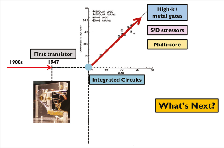
Figure 1. Innovation in process integration is the real enabler of Moore’s law
Multi-gate architectures
Mitigation of short-channel effects can be realized with a gate-all-around nanowire FET architecture, which provides superior electrostatic control (see Figure 2). A full circuit architecture is yet to be developed, but vertical channel designs are offering a compact footprint, constrained by the contacted-gate pitch. There is the possibility to relax physical gate length and even channel thickness with respect to lateral nanowires or FinFETs.

Figure 2. Different device architectures: triple-gate finFET, lateral gate-all around nanowire FET (GAA-NWFET) with one or more wires stacked horizontally on top of one another, and vertical GAA-NWFET with multiple wires stacked vertically next to each other. Figure taken from A. Veloso et al. ECS Trans. 2016
This new architecture is not just a solution for silicon. In fact, it offers even more promise for III-V channels, as they are severely challenged by channel thickness scalability, due to much stronger size-quantization effects. This issue stems from the lighter isotropic bulk electron effective mass for III-Vs than for silicon.
One of the most promising emerging devices is the tunnel FET, which could lead to far lower operating voltages. For this form of transistor, it makes sense to employ vertical channels, due to the need for complex epitaxial heterojunctions and the asymmetric source-drain overlap. Given this state of affairs, there is a need to investigate methods for realising highquality III-V vertical nanowire devices. At imec, we are pursuing this, with efforts directed at addressing the rising demand for innovations in process integration.
Any attempts at developing these alternate channel devices must use the silicon substrate as the foundation. Taking this approach ensures that the technology can take advantage of the mature silicon CMOS process, and enable co-integration of different functionalities. The challenge is that the growth of III-Vs on silicon is not easy: these are two markedly different material systems, with mismatches in lattice constants, thermal expansion coefficients and polarities.
Our focus is the investigation of InGaAs vertical nanowire devices, produced with an ‘industry-friendly’ approach. The idea is to grow stacks of InGaAs inside trenches, defined in a 300 mm diameter silicon wafer, before a top-down technique is applied, creating nanowires with diameters down to 30 nm using patterning and dry-etching steps. However, to speed our development, we have begun by using InGaAs grown on a lattice-matched InP substrate, to ensure good quality layers.
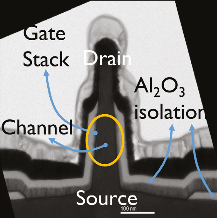
Figure 3. Tunnelling electron microscopy image of a typical vertical In0.53Ga0.47As nanowire device fabricated by imec. The key components of a device are marked.
To study the electrical properties of these highmobility channel materials, we form a semiconductor surface with a low density of defects. We meet this requirement with a process scheme that allows us to investigate nanowires that are dry etched from high-quality InGaAs layers grown on lattice-matched substrates (see Figure 3). Note that our dry etching does not damage the surface, but ensures a good channel-oxide interface; and it provides a vertical sidewall profile without any tapering, leading to superior electrostatic control.
Establishing a manufacturing process for the vertical nanowire III-V devices has to begin with efforts to understand the impact of the dimensions of the nanowire on the electrical properties of the channel, and its compatibility with high-κ dielectrics. While these issues are not a consideration for many research groups, they need to be addressed before production of devices is feasible.
Before manufacture can even be considered, it is essential to establish VLSI-compatible, uniform process flows for vertical gate-all-around devices. They must also be compatible with high-κ dielectrics. One key question is this: Does the reliability of the gate stack change with the introduction of threedimensional devices? Additional concerns relate to the parasitic source and drain resistances. How do the nanoscale contacts behave in a nanowire set-up? Another issue with vertical devices is the reduction in the access resistance and the contact resistance to the source/drain regions. Failure to address this can severely limit device performance.
We are trying to address all of this, and our starting point is to undertake an effective comparison of devices across different maturity levels, using a figure of merit called the Q factor: it is the ratio of transconductance (Gm) for on-state performance to the sub-threshold swing (SS) for switching efficiency. For our single vertical nanowire transistors, the Q factor is 21, one of the highest reported values for this class of device (see Figure 4).
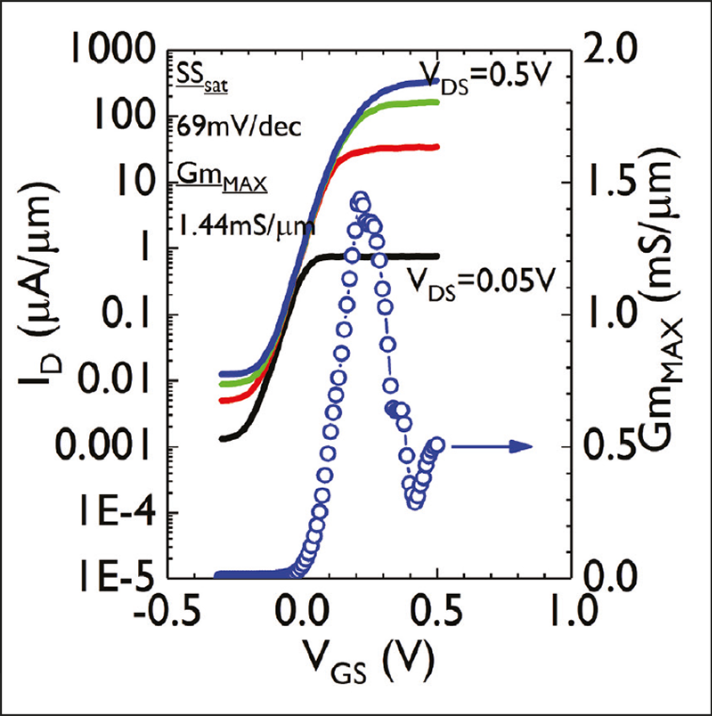
Figure 4. Normalized IDVGS of a single 30 nm-diameter device with best value for Q, which is the ratio of transconductance to sub-threshold swing.
In this device, the drive current increases by more than two orders of magnitude when the drainsource voltage is raised from 0.05 V to 0.5 V. This difference is caused by a Schottky barrier at the vertical nanowire top contact. This barrier, which is formed at the interface between the drain metal and InGaAs, increases as the nanowire diameter shrinks, highlighting the challenges associated with scaling this transistor.

Unfortunately, the access resistance in vertical devices is influenced by the three-dimensional nature of the device, but this is not captured in typical planar test structures. What’s needed is a dedicated test vehicle – addressed, in our case, with a vertical nanowire resistor, formed with a common process flow, that enables investigation of the n+ drain contact to the vertical nanowire MOSFET. Using data extracted from resistor measurements, in combination with Sentaurus Device simulations, we obtain a better understanding of the contact resistance and can predict this impact. In addition, we have a better insight on channel surface passivation, and the impact of interface states on the performance of the vertical nanowire MOSFET.
What we have learned with this approach can play a crucial role in the future of CMOS logic. We have discovered that a significant boost in performance results from reducing the Schottky barrier height at the vertical nanowire contact (see Figure 5).
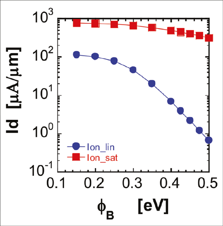
Figure 5. On-state performance prediction from device simulations.
Throughout the development of III-V MOSFETs, the gate stack has provided a significant challenge. Back as 1965, when a team at the Radio Corporation of America started to develop a GaAs MOSFET, they abandoned the project due to the lack of a defect free gate oxide. Progress has followed, using a combination of surface passivation and the addition of a gate dielectric, via atomic layer deposition.
However, there is still much work to do. The on-state performance of the device is hampered by a new challenge in the form of oxide traps in the high-κ dielectric. In InGaAs channel devices, Al2O3-based dielectrics are often used, thanks to a self-cleaning effect during atomic layer deposition. When deposition begins, most III-V surface oxides are reduced, giving rise to a good quality interface – even in the absence of any surface treatment or any in-situ oxide deposition after III-V growth. However, the oxide is still not free of traps.
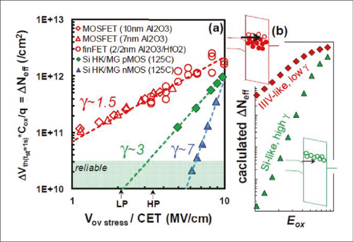
Figure 6. (a) Charge trapping density (ΔNeff) as a function of equivalent oxide field (EOX). The voltage dependence (γ ~ 1.5) is consistently weaker than that for silicon, due to (b) a wide distribution of oxide defect levels around the InGaAs conduction band minimum. Figure taken from J. Franco et al. IEDM 2017.
An indication of carrier-defect energy alignment is provided by measurements of the stress voltage dependence of the threshold voltage – that is, the shift in threshold voltage with applied operating voltage. Unlike silicon devices, Al2O3-based III-V devices, with an effective oxide thickness ranging from 5 nm to 1.4 nm, have a relatively weak voltage dependence of the charge trapping density, computed from the change / shift in threshold voltage (see Figure 6(a)). That’s because traps in Al2O3 are energetically located in the upper half of its bandgap, with a wide distribution peak above the conduction band edge of InGaAs (see Figure 6(b)). The location of these traps influences the characteristics of n-channel devices.
Holding back progress with vertical nanowire MOSFETs is the absence of study on the impact of processing and architecture on charge trapping in the gate dielectric. We are addressing this omission with an investigation of effective charge trapping in an Al2O3-based gate stack for InGaAs vertical nanowire devices. This effort has revealed that the charge trapping density in III-V vertical nanowire devices is comparable to that of nanoscale InGaAs devices with similar Al2O3-based gate stacks, such as finFETs, lateral gate-all-round devices and TFETs (see Figure 7). We have also found that we can reduce the defect density in the oxide and increase device performance by annealing transistors in forming gas, a mixture of 5 percent hydrogen and 95 percent nitrogen.
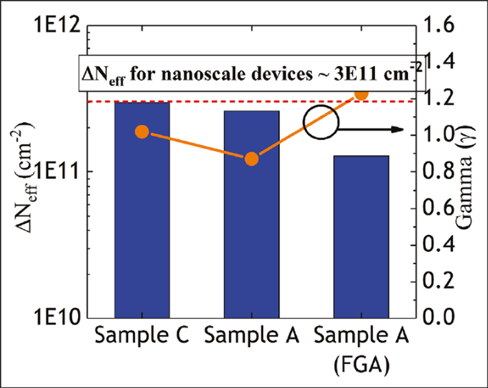
Figure 7. Sample A and Sample C are Nanowire MOSFET devices, with and without an ammonium sulphide treatment to the channel respectively, before gatestack deposition. We see that irrespective of the treatment the defect density is constant and only changes with an anneal, implying that these defects / traps are predominantly present in the gate oxide and not in the channel surface. The ΔNeff for III-V vertical nanowire devices is comparable to other nanoscale InGaAs devices. Forming Gas Anneal (FGA), a mixture of 5 percent hydrogen and 95 percent nitrogen, maximizes the improvement in terms of ΔNeff and g.
Marching to manufacture
Our results make a compelling case for our device as an industrial technology. There is good reason to believe that the gate stack is reliable: firstly, moving to a vertical nanowire architecture, we see no penalty in gate stack reliability; secondly, the combination of a dry etch and various surface treatments does not introduce significant defects to the channel surface or impact gate stack deposition; and thirdly, the gate stack quality, in terms of charge trapping, does not degrade with scaling of the equivalent oxide thickness. In fact, a marginal improvement results from the forming gas process, alongside a significant boost in device performance.
We anticipate that better nanowire contacts can improve our devices by a factor of two or three. With the help of our in-house developed test structures, we aim to undertake further study on the impact of nanowire dimensions on these contacts. Our ultimate goal is to realize the full-potential of high-mobility channel materials for future technology nodes.
Further reading:
S. Ramesh et al. Record performance Top-down In0.53Ga0.47As vertical nanowire FETs and vertical nanosheets, Electron Devices Meeting (IEDM), 2017 IEEE International
A. Milenin et al. Microelectronic Engineering 2018
Low temperature MBE yield high-quality InAs quantum dots on a SiO2-on-silicon substrate
Researchers at The University of Electro-Communications, Japan, are claiming to have broken new ground by forming the first high-quality InAs dots on SiO2-on-silicon substrates.
InAs dots on SiO2 have been reported as far back as 2007, by a team at the Institute of Nanotechnologies in Lyon, France. However, those dots failed to luminescence, while the ones made by the team in Japan exhibit excellent crystallinity and produce a strong photoluminescence peak.
An important aspect of the latest work is that it introduces greater freedom in the fabrication of the dots, giving them the potential to serve in a wider variety of applications. According to team spokesman Koichi Yamaguchi, the dots could be used for silicon photonics, photovoltaics, memory, and display devices.
In Yamaguchi’s view, the key to producing these high-quality dots is controlling the single nucleation of InAs islands on the surface of the silicon oxide. “In particular, we paid attention to control precisely the molecular beams of indium and arsenic.”
As well as forming the dots on SiO2 on silicon, the team produced them on a silicon oxide layer deposited on GaAs. The motivation is to understand how these dots form, and to be able to produce them on many different platforms. “Now, we are also trying to fabricate other III-V quantum dots on silicon oxide films, deposited on other substrates,” says Yamaguchi.
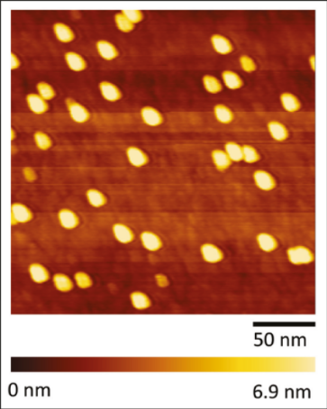
An atomic force microscopy image of InAs dots on silicon oxide on silicon.
He and his co-workers produced their dots via the Volmer-Weber growth mode, which involves forming threedimensional islands from the outset. Due to this, there is no wetting layer. That is advantageous, because it creates a system that is only zerodimensional, rather than one that combines this with a two-dimensional system.
Thermal oxidation creates SiO2-on-silicon substrates, which have a 1 μm-thick SiO2 film, while RF magnetron sputtering provides the deposition of a 0.5 μm-thick silicon oxide film on GaAs.
Both these structures provided platforms for the growth of InAs dots by solid-source MBE. For the GaAs-based platform, thermal cleaning under an arsenic pressure at 590 °C preceded the growth. For both types of foundation, after InAs dots were formed at temperatures of between 350 °C and 400 °C, using a growth time of 120 s and a growth rate of 0.05 monolayers per second, thermal annealing took place under arsenic pressure at the growth temperature.
Scrutinising the surface of the samples with an atomic force microscope revealed that the dots are individually deposited, and on both platforms the size and density of the dots are very similar. On silicon oxide on GaAs, the dot density is 5.9 x 1010 cm-3, while on SiO2 on silicon it is 6.7 x 1010 cm-3.
The researchers used the volume and density of the dots to gain an insight into the growth process. They found that as growth temperature increases, the product of the average volume and density of the dots decreases exponentially, due to re-evaporation of adatoms. This finding highlights the need for a low growth temperature.
Analysing samples with transmission electron microscopy revealed that each dot is a single crystal grain with a different crystal orientation.
With a height of 3 nm to 8 nm and a length of 5 nm and 13 nm, according to atomic force microscopy, the size of the dots is below the de Broglie wavelength in InAs. This means that the dots are expected to behave as a zero-dimensional system.
Photoluminescence measurements produce a peak at 1.22-1.23 eV. Simulations with APSYS software suggest that this is associated with a first excited state transition involving a heavy hole.
Yamaguchi and co-workers are planning to expand the capabilities of their MBE process, so that they can fabricate other III-V quantum dots on silicon oxide films, which may be deposited on other substrates. They will also try to improve the quality of their dots, to aid their adoption in devices.
Reference
A. Makaino et al. Appl. Phys. Express 11 0855501 (2018)

Lowering the growth temperature for the GaN cap yields promising InN
Indium Nitride has many attractive attributes. It has the highest electron mobility of the III-Ns, making it a promising material for high-frequency and high-speed optoelectronic devices; and its bandgap of 0.7 eV enables the nitrides to span the UV to the near infra-red.
Growth of InN is challenging, with material tending to be plagued with nitrogen vacancies that result in a high concentration of residual electrons. But it doesn’t have to be that way, according to recent work by a team from NTT Basic Research Laboratories, Japan – they have used MOCVD to produce InN heterostructures with a high crystal quality.
The team’s heterostructures are formed by sandwiching a 30 nm-thick layer of InN between two layers of GaN.
Other teams have produced similar structures with InGaN barriers, but these have less promise, according to team spokesman Tetsuya Akasaka. He argues that the higher bandgap discontinuity associated with GaN barriers could allow InN devices to operate at room temperature.
“In addition, InGaN has a miscibility gap. Consequently, in principle, the crystal quality of GaN should be better than InGaN.”
To produce their devices, the team discarded the rule book for GaN growth. Instead of adhering to the widely held view that the GaN cap must be grown at a higher temperature than the InGaN layer, they used a lower temperature.
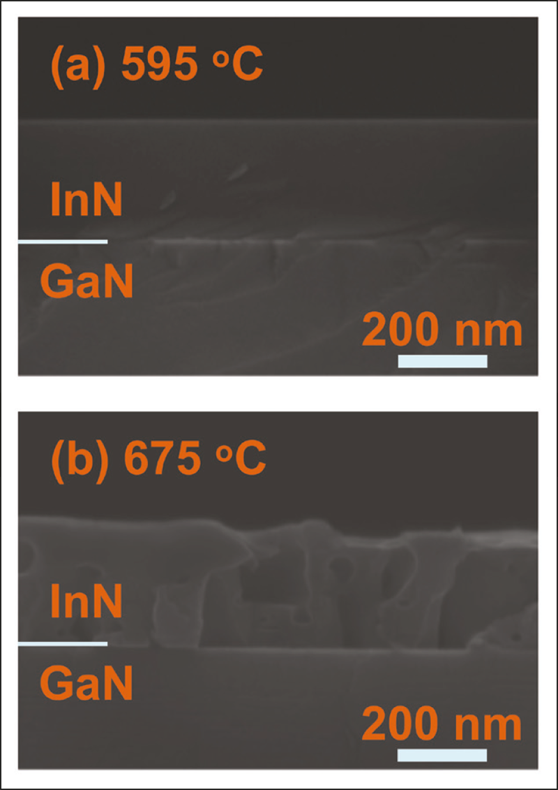
Scanning electron microscopy reveals the voids in InN that appear at higher growth temperatures
Another key to their success has been the use of substrates with a nitrogen face rather than a gallium face. The former prevents nitrogen from evaporating from the growing surface, enabling an increase in the growth temperature of InN by about 100 °C.
Production of the team’s heterostructures began by loading a commercially available N-face GaN(0001) bulk substrate into a vertical MOCVD reactor. This material, which Akasaka says has a price that is almost the same as that for a gallium-face GaN substrate, has an electron concentration in the region of 1018 cm-3 and a threading dislocation density below 5 x 106 cm-3.
Using a reactor pressure of 300 Torr, the researchers produced several single and double heterostructures, using a range of growth temperatures.
The portfolio of single heterostructures revealed that increasing the InN growth temperature from 595 °C to 675 °C changed the morphology of the InN surface from one that is smooth to one that fails to fully coalesce the GaN buffer. According to the team, the voids associated with high-temperature growth could be attributed to the etching of InN by atomic hydrogen, produced during decomposition of ammonia.
To evaluate crystal quality, the researchers recorded photoluminescence at 83K. They found that the higher the growth temperature, the stronger the peak and the longer its wavelength.
This shift in wavelength is attributed to the electron concentration, which falls from 1 x 1020 cm-3 for the sample grown at 595 °C to 4 x 1018 cm-3 for that grown at 675 °C. Akasaka says that the lower concentration is acceptable for applications such as LEDs. “However, we should decrease the residual electron concentration for transistors.”
The team’s next step involved the growth of an InN double heterostructure at 675 °C, a temperature that is good for intense photoluminescence, but far from ideal for good film coverage. Imaging identified voids in the InN layer and a rough interface with GaN.
To address this poor morphology, the researchers maintained the temperature for the InN layer, but reduced that for the GaN cap to 550 °C. This paid dividends, eliminating the voids and creating very abrupt interfaces. Note that further decreases in temperature are detrimental to the photoluminescence intensity, possibly because crystal defects are formed in the GaN cap that act as non-radiative recombination centres.
The researchers are now studying step-free InN LEDs emitting in the red, green and blue. Back in 2012, they produced a step-free InN quantum well with an InN thickness of one monolayer that emitted in the violet.
“A theoretical calculation suggests that two- and threemonolayer- thick, step-free InN quantum wells can emit green and red, respectively,” says Akasaka. Make these and the monolithic integration of red, green and blue LEDs could follow.
