


If you are a regular reader of this magazine, there’s a good chance that you can recall why the makers of blue and green LEDs and lasers advocate the use of very thin quantum wells.
It’s a relatively simple argument, which centres around the strong internal electric field in these optoelectronic devices, arising from the piezoelectric nature of the InGaN wells and GaN barriers. This field pulls apart electrons and holes, so to ensure a sufficient overlap and ultimately a healthy degree of radiative recombination, the wells must be no more than a few nanometres thick.
This oft-repeated argument is not being disputed – but it fails to tell the whole story. Why? Because it only considers ground state transitions between electrons and holes.
Take into account the excited states and you’ll come to a different conclusion, as the Polish team from the Institute of High Pressure Physics and TopGaN have found. Their simulations show that at typical current densities found in a laser, the overlap between the first excited states in a 10 nm-thick quantum well is even higher than the overlap of ground states in wells just a few nanometres thick.
So what, you may say. After all, aren’t thicker wells known to be riddled with dislocations, as well as being plagued with variations in thickness and compositional uniformity?
It’s a fair point, but these issues are not insurmountable. All that’s needed is a better substrate, found in the form of GaN grown by the ammonothermal method. Building on this foundation, the lasers that have been made by the Polish team have a remarkably low density of threading dislocations, and feature wells with great uniformity.
Thanks to these attributes, the lasers with the thicker wells have the edge over their more conventional siblings. Ridge-waveguide designs with a 10 nm-thick well have a differential gain that is about 30 percent higher than variants with three, 2.6 nm-thick wells.
The work by the team gives more freedom to the designers of GaN-based lasers. However, it remains to be seen if it can have a big impact on commercial production. Manufacturing GaN substrates by the ammonothermal method is far from easy, while the quality of this foundation could well be the key to making high-quality InGaN-based lasers with thick quantum wells.

Worldwide LED video display area shipments are expected to increase by 36.7 percent in 2019 as factors including plunging prices make them a more attractive alternative to projectors and flat panel displays, according to IHS Markit.
Global LED video display area shipments are set to reach 1.1 million square meters in 2019, up from 800,000 in 2018. This follows shipment growth of 83 percent in 2018. Revenue this year will amount to $5.1 billion, compared to $4.8 billion last year.
By 2023, area shipments will expand to about 2 million square meters and $7.5 billion in revenue.
“LED video display technology is rapidly replacing front projectors in large venues,” said Tarika Bheda, research and analysis associate director at IHS Markit. “The technology is also aggressively competing with LCD videowalls in indoor applications, such as command-and-control rooms and premium conference rooms. In addition to declining cost, lifespan, size scalability and seamless image display are the main factors driving the increasing adoption of LED video technology.”
Nearly 50 percent of LED video displays shipped this year will be installed in indoor applications, with the 2-to-4.99mm pixel-pitch category dominating the market.
“Pixel-pitch innovations and price erosion are continuing to make LED video-display technology more affordable for indoor applications,” Bheda added.
IHS Markit predicts the 2-to-4.99mm pixel-pitch category will grow to a 52 percent share of the global LED video display market in 2023, up from 40.0 percent in 2019. During the same time period, the share of the smaller-than-or-equal-to 1.99mm pixel-pitch category will expand to 13 percent, up from 9.0 percent.
The smaller-than-or-equal-to 1.99mm pixel pitch category is where most of the innovation is taking place. More brands are now venturing into this space. Sellers of projectors and legacy flat-panel displays are expanding their product lines to include fine-pixel-pitch LED video displays to cater varying customer demands.
LED video display suppliers have increased their manufacturing capacity significantly during the last few years. Competition among brands has intensified, pulling average selling prices (ASPs) lower. However, revenue growth is projected to remain positive as ASP erosion will be balanced by an increase in demand for expensive fine pixel-pitch displays.
In terms of applications, public spaces remain the biggest unit and revenue contributor for the LED video display market, with a share of more than 40 percent in 2018. IHS Markit expects the public-space application to remain on top, while transportation, control room and corporate will grow at the fastest pace during the forecast period between 2019 and 2023.
LED video display manufacturers are moving toward standardisation, so they are devising preconfigured and easy-to-install products to address the needs of certain vertical markets, where standard designs are preferred. These markets include corporate boardrooms, which don't require Regionally, China led the LED video display market with a 34 percent share of shipments in 2018, followed by North America at 22.4 percent and Western Europe at 13 percent. These regions are expected to maintain similar shares in 2019 with North America declining slightly to 19.6 percent due to US-China tariff conflict, which led to lower-than-expected results in the first quarter of 2019.
The Chinese market is thriving because of smart-city initiatives undertaken by local governments. North America leads in terms of volume due to large outdoor sports and public-space projects, which together account for more than 50 percent of total shipments. Western Europe brings significant demand from digital-out-of-home (DOOH) projects. LED video demand in Asia pacific is split between countries with high adoption rates—including India, Australia, Thailand and South Korea—and nations that have strong growth potential.
IHS Markit expects the Asia Pacific region to expand, as established brands develop their sales structures. Shipments in 2019 are expected to rise by 70.0 percent compared to 2018. Japan's LED video display shipments are expected to get a boost in 2019 as the country prepares for 2020 summer Olympics. creative designs.
Alta Devices has announced it is scaling up production of its GaAs solar cells to meet growing demand for small satellites (SmallSats). Tens of thousands of low-earth orbiting (LEO) SmallSats are expected to be launched over the next decade. They will all rely on the sun for power. Alta Devices solar material has the potential to meet the specific needs of this SmallSat boom.
Solar is the single most expensive hardware component in a small satellite. Alta Devices has developed a proprietary process to mass produce its thin film GaAs technology. The production equipment is being scaled up to produce at much higher volumes and lower cost than other space solar manufacturers. Alta's ability to produce at this scale could substantially lower the cost of each SmallSat.
Furthermore, Alta Devices flexible solar cells provide a new level of mechanical and design flexibility for the satellite industry. Alta's technology can be mounted to thin, flexible, low-mass deployable structures allowing creative design approaches to maximising the solar array. These include coiled carbon fibre booms, flat-packed, polymer-based accordion-style arrays, or even inflatable structures. This allows more compact design of the high-power solar arrays required to power high-speed LEO communication satellites.
Traditional photovoltaic assemblies (PVAs) are composed of hundreds or thousands of small solar cells, each protected with a tile of glass, connected to each other through individual metallic welds, which are then carefully grouted to prevent electrical arcing and attack from the space environment. In contrast, Alta's space product will consist of flexible, glass-free units that are 10 to 100 times larger, thus eliminating breakage, lowering cost and having no exposed electrical interconnects. Alta says its space product will enable bonding to customer substrates using a large-area, high-volume vacuum bonding process, as opposed to mounting individual cells or CICs (Coverglass Interconnected Cells).
Overall, Alta's goal is to provide LEO satellite manufacturers with a better balance of solar conversion efficiency, reduced array weight, cell durability, speed of deployment, and cost compared with conventional space solar cells.
According to filings disclosed by the US Federal Communications Commission, over 15,000 LEO SmallSats are planned for deployment in the near future. The applications of these satellites include communications, scientific research, military intelligence, remote sensing, and new technology development.
Over the coming years, Alta Devices plans to produce tens of megawatts of solar. Manufacturing will take place at Alta Devices corporate facility in Sunnyvale, California and at an international manufacturing facility. In April this year, Alta Devices solar was used on a successful mission to power over 60 ThinSats launched from the NASA Wallops Flight Facility in Virginia. Alta Devices is working with top satellite manufacturers for the deployment of its technology on several upcoming launches.
Alta Devices CEO, Jian Ding stated: “Now that we are established in the HALE UAV/HAPS market, we are committed to enabling LEO satellite projects with our unique technology. We believe our solution will meet the needs of this fast-growing market.”
Cree and ON Semiconductor have announced the execution of a multi-year agreement where Cree will produce and supply its Wolfspeed SiC wafers to ON Semiconductor.
The agreement, valued at more than $85 million, provides for the supply of Cree's advanced 150mm SiC (SiC) bare and epitaxial wafers to ON Semiconductor for use in high-growth markets, such as electric vehicle and industrial applications.
“ON Semiconductor continues to be a leader in driving the development of energy efficient innovations and devices,” said ON Semiconductor VP and chief procurement officer Jeffrey Wincel. “Partnering with Cree is essential in maintaining a world-class supply base. This agreement supports our commitment to growing automotive and industrial applications and ensuring the availability of industry-leading SiC that helps engineers solve their unique design challenges.”
“We are committed to leading the global semiconductor market's transition from silicon to SiC solutions and are pleased to support ON Semiconductor as we work to accelerate this market,” said Cree CEO Gregg Lowe. “This is the fourth major long-term agreement for SiC materials that we have announced in the past year and a half. We will continue to drive SiC adoption and availability through ongoing wafer supply agreements, such as this, and our recently announced major capacity expansion.”
LED firms Everlight and Nichia are both claiming victories over a series of courtroom wrangles about patents.
Taiwanese Everlight has issued a press statement announcing successful invalidation trial procedures in a number of countries against a range of YAG patents filed by its Japanese rival Nichia. These procedures include the US Supreme Court's decision that the claims of Nichia's US YAG patents US5,998,925 and US7,531,960 were invalid; and the Full Court of the Federal Court of Australia's decision that the claims of Nichia's Australia YAG patent 720234 were invalid.
In addition, Everlight says that on May 9, 2019, Beijing IP Court decided that Nichia's China YAG patent CN200610095837.4 was invalid; and on April 25, 2019, the Taiwanese Supreme Administrative Court decided that Nichia's Taiwan YAG patent TW383508 was invalid.
Meanwhile, Nichia has issued its own statement. It says that the China National IP Administration (CNIPA) has affirmed a patent invalidation request filed by Nichia against Chinese patent ZL200710161547.X (547 Patent) in relation to flip-chip technology owned by Everlight Electronics (China). Nichia states that after the CNIPA's decision, infringement lawsuits concerning the ‘547 Patent filed by Everlight against Nichia before the Shenzhen Intermediate Court were terminated by Everlight's withdrawal.
In January 2019, Nichia won infringement lawsuits, based on a YAG patent, against Everlight and its distributors in China. Nichia says that the judgment was final, and Nichia received damages of around $460k (RMB 3.2 million) from Everlight and its distributors.
In response to Nichia's press release, Everlight has declared: “We finally decided to withdraw the statements of the lawsuit without prejudice based on the adjustment of the litigation strategy, but the above-mentioned winning facts remain unchanged.”
Plessey has appointed Edward H. Frank to its microLED advisory board, as part of the rapid development of the company's microLED technology.
Keith Strickland, co-CEO and CTO at Plessey, said: “Ed's strong and proven history of developing and bringing revolutionary solutions to market makes him an excellent addition to our advisory board. His expertise in delivering innovative silicon and systems, at companies both large and small, will be invaluable as we continue to provide cutting-edge microLED display solutions to AR applications.”
Frank commented: “MicroLED display has many advantages such as high brightness, ultra-low power consumption, fast response time, very high contrast rate, wide colour gamut, long lifetime, environmental stability, high resolution, the option of flexible backplanes and integration of sensors in the display. Its main challenges are manufacturing complexity and yield issues, all of which Plessey are addressing, I am excited to be working with such an innovative, cutting-edge technology company.”
Previously, Frank was CEO and co-founder of Cloud Parity, a voice-of-the-customer start-up. Earlier, he served as VP of Macintosh Hardware Systems Engineering at Apple, as corporate VP of R&D at Broadcom, a broad-based manufacturer of wireless chips used in many Apple devices and served as a distinguished engineer at Sun Microsystems.Frank currently serves on the boards of Analog Devices, and Marvell.
Frank earned a BSEE and MSEE from Stanford University, and a PhD in computer science from Carnegie Mellon University, where he is presently Vice-chair of its Board of Trustees. He is a member of the National Academy of Engineering in the United States and is a named inventor on over 50 patents.
The US Army has awarded Lockheed Martin three contracts to produce additional Q-53 radars and outfit the GaN-based systems with enhanced capabilities, including extended range and counter unmanned aerial system (CUAS) surveillance.
"We realise the warfighter needs new and improved capabilities. The Q-53 represents a fast path to respond to current and emerging threats," said Rick Herodes, director of the Q-53 program at Lockheed Martin. "The flexibility of the architecture continues to allow the Q-53 to provide capabilities far beyond the original mission and allows for additional upgrades in the future."
The Army awarded Lockheed Martin a contract for a third lot of 15 Full Rate Production systems. Once this contract is delivered the Army will own 189 Q-53 systems. The Lot 3 systems will continue to be produced using GaN transmit-receive modules. This will provide the radar with additional power, reliability and the possibility for enhanced capabilities including extended range, counterfire target acquisition (CTA) and multi-mission, which delivers simultaneous CTA and air surveillance.
The primary mission of the Q-53 is to protect troops in combat by detecting, classifying, tracking and identifying the location of enemy indirect fire in either 90 or 360-degree modes. The Q-53 has protected warfighters around the world since 2010.
Lockheed Martin uses an open GaN foundry model, using relationships with commercial suppliers that use the power of the expansive telecommunications market to provide military-grade GaN modules while taking advantage of commercial cost efficiencies.
Akash Systems, a San Francisco-based GaN-on-diamond startup focused on satellite communications, has announced $14.5 million in Series A funding, including $10 million in new equity funds, and an additional $4.5 million converted from prior convertible notes.
Investors in this round include Khosla Ventures, Founders Fund, ACME Capital, Sriram Krishnan, Correlation Ventures and others. Akash will deploy the new capital toward scaling its transmit/receive radio modules and power amplifier business, moving it closer to profitability.
“The successful close of this funding round marks an important next step in fulfilling Akash's mission statement,” said co-founder, CEO and GaN-on-diamond Inventor Felix Ejeckam. “Our aim is to be the RF communications link for every satellite in space.”
Akash has designed its satellite transmit/receive radio modules to easily integrate with existing ground station and satellite infrastructure for satellite makers in all markets. The company's radios, which are expected to be available for purchase in late 2019, promise impressive performance not yet seen on the market.
“Akash Systems is playing a critical role in meeting the growing and vital need for improved satellite communications infrastructure,” said Delian Asparouhov of Founders Fund, which is focused on assisting entrepreneurs to build impactful new energy and technology companies. “We're proud to be part of Akash's journey as a critical enabler and accelerant in global communications.”
“It's rare to see a young company with such transformative technology already approaching commercialisation,” said Alex Fayette of ACME Capital. “Akash's business lies squarely at the intersection of major trends like global connectivity, high-performance telecommunications and space-based infrastructure. Their foundational technology will underpin other solutions across these industries. We are thrilled to partner with the team at this early stage as they execute against their vision.”
“What Akash has been able to achieve in its first few years is remarkable, as it has already attracted major customers across the ecosystem. The company is quickly shaping trends in global telecommunications. It's one of the most exciting companies we've seen in a while,” said angel investor Sriram Krishnan.
In GaN-on-Diamond, the hottest part of a transistor is brought to within tens of nanometers of synthetic diamond - the most thermally conductive material ever made by humans. The result is a dramatic reduction in the waste heat generated from the power amplifier, and therefore the entire satellite system; in the communications “base stations” of space, the RF power amplifier is typically responsible for the bulk of the power consumed and the heat generated. The cooler state of operation gives RF and satellite system designers a previously unattainable thermal envelope to dramatically improve a satellite's communication bandwidth and energy efficiency while simultaneously shrinking the system's size, weight and operating costs.
Akash is currently manufacturing GaN-on-diamond-based power amplifiers and radio modules for customers who make satellites requiring high frequency and high power efficiency. Its radio products are on track to hit the market in Q4 2019.
Australian semiconductor company BluGlass has announced that the United States Patent and Trademark Office has issued US Patent 10,355,165, Buried Activated p-(Al,In)GaN Layers. This proprietary technology has significant performance potential in a number of applications including high-brightness LEDs, micro-LEDs, laser diodes, solar cells, and other optoelectronic and power electronics devices.
BluGlass' RPCVD-grown buried activated p-GaN layers can help address one of the LED industry's critical challenges: “efficiency droop”. The efficiency of an LED is a measure of how much light output is generated for a given amount of electrical power used to drive the device. Efficiency droop is where the efficiency of an LED reduces as operating power is increased. This challenge results in many of today's high-powered LEDs being operated outside their peak efficiency.
Incremental efficiency improvements continue to be a major objective for LED manufacturers.
One potential resolution of efficiency droop is multi-junction or cascade devices (LEDs or laser diodes as examples). RPCVD's buried activated p-GaN layers are a critical building block to enable the tunnel junction, which in turn allows multiple LEDs to be grown in a continuous vertical stack and interconnected in a single, high efficiency chip, called a cascade LED. As a result, less power is needed to deliver the desired light output, potentially eliminating efficiency droop and significantly increasing device performance.
Cascade LEDs are expected to enable smaller, cheaper and higher performing LEDs - the three key interest areas of the LED industry. To date, functioning tunnel junctions, and therefore cascade LEDs, have been prohibitively difficult to produce due to the challenges in achieving buried activated p-GaN using conventional growth technologies such as MOCVD.
BluGlass is developing and commercialising a unique Australian technology called remote plasma chemical vapour deposition (RPCVD), a revolutionary approach to the manufacture of group III nitrides which are essential components used in millions of electronics devices globally. RPCVD offers better-performing, lower-cost devices and more environmentally sustainable processes for electronics manufacturers producing LEDs for automotive and overhead lighting, microLEDs for wearables and virtual reality display and power electronics for efficient power conversion.
BluGlass' Managing Director, Giles Bourne said “This patent adds an important cornerstone to BluGlass' intellectual property portfolio, protecting our unique RPCVD process, hardware and competitive advantages. RPCVD allows us to develop this elegant new option for resolving the challenges of efficiency droop in high-performance LEDs - something that's been very difficult to resolve using the industry standard MOCVD technology.” “Our growing strategic patent portfolio, comprising 63 internationally granted patents, continues to underpin the commercialisation of our RPCVD technology across a range of market segments with long-term market exclusivity”. BluGlass has received strong interest on the performance potential of RPCVD tunnel junctions and cascade LEDs from the industry. Discussions with a number of groups are continuing.
The Superior Court of California has granted Lumileds a permanent, worldwide injunction against Elec-Tech International (ETI), immediately prohibiting ETI and its affiliates from using, disclosing, licensing, or selling Lumileds' epitaxy technology trade secrets that ETI was found to have misappropriated.
The injunction also prohibits ETI from manufacturing, distributing, importing, exporting, or selling any products that use certain of ETI's own epitaxy growth recipes that the jury concluded were produced using Lumileds' trade secrets.
This injunction is the result of a bench trial (following last August's jury trial), where Lumileds presented experts and significant evidence that clearly demonstrated the appropriateness of a permanent worldwide injunction.
The Court specifically found that Lumileds' trade secrets continue to exist and are valuable. The Court determined that without an injunction, ETI would continue to misappropriate Lumileds' trade secrets and further stated that if ETI continued to use the stolen intellectual property, Lumileds would suffer irreparable harm. Furthermore, the Court has denied ETI's motions for a new trial and to set aside the verdict awarded by the Jury.
“We are very pleased with the Court's determination that a permanent injunction is warranted in this case as it further validates the jury's findings from the 2018 verdict,” said Cheree McAlpine, chief legal officer and SVP of Lumileds. “Protecting our innovations is paramount to our business, and we will continue to vigorously defend our intellectual property.”
After a four-week jury trial beginning in July 2018, a jury of 12 people found that ETI misappropriated and used five Lumileds' trade secrets related to epitaxy technology. These trade secrets include the foundational epitaxy-development technology used by Lumileds to produce its LEDs.
The jury determined that ETI used Lumileds' trade secrets in six of their recipes and the misappropriation and use of Lumileds' trade secrets was a substantial factor in causing ETI to have obtained an unjust benefit of $66 million.
Infineon Technologies utilizes the ANPC topology for its hybrid SiC and IGBT power module EasyPACK 2B in the 1200 V family. Optimising for sweet spot losses of the CoolSiC MOSFET and the TRENCHSTOP IGBT4 chipsets respectively, the module features increased power density and a switching frequency of up to 48 kHz. This is especially well suited for the needs of new generation 1500 V photovoltaic and energy storage applications. The new ANPC topology supports a system efficiency of more than 99 percent. Implementing the hybrid Easy 2B power module in for example, the DC/AC stage of a 1500 V solar string inverter allows for coils to be smaller than with devices with a lower switching frequency. It therefore weighs significantly less than a corresponding inverter with purely silicon components. Additionally, the losses with silicon carbide are smaller than with silicon. For this reason, less heat must be dissipated so that the heat sink can also shrink. Overall, this leads to smaller inverter housings and costs savings at system level. Compared to 5-level topologies, the 3-level design reduces complexity of the inverter design.
The Easy 2B standard package for power modules is characterised by an industry-leading low stray inductance. Additionally, the integrated body diode of the CoolSiC MOSFET chip ensures a low-loss freewheeling function without the need for another SiC diode chip. While the NTC temperature sensor facilitates the monitoring of the device, the PressFIT technology reduces assembly time for mounting the device.
Wafer firm IQE has started initial VCSEL production for a second major customer at the Newport Mega Foundry in Wales and further positive qualifications.
Initial production has now commenced with a second major customer, serving the Android supply chains, and several more are in advanced stages of qualification. Performance data from the Newport Foundry has exceeded previously attained performance levels, and several new qualifications are now in long term reliability testing.
As a result, IQE has signed a contract extension with one of its largest VCSEL customers, extending the current contract until the end of 2021. In addition, two other existing contracts have also been extended with several other new contracts in final negotiations.
VCSELs are a key component in multiple current and future 3D sensor systems, using both structured light and Time of Flight (ToF) technologies. Applications range from 3D Facial Identification (front facing) systems and world facing cameras on mobile handsets to LiDAR and in cabin sensing for autonomous drive vehicles, range-finding and 3D sensing systems for a wide range of industrial and commercial applications.
Production volumes are expected to ramp strongly over the next few years as adoption across multiple mobile platforms and other use cases proliferate. In anticipation of such strong growth, IQE has invested heavily over the last two years in building the worlds's largest VCSEL epi-wafer facility in Newport, UK (IQE's Mega Epi Foundry). IQE is involved in multiple engagements across all of the aforementioned applications and is currently qualifying more than a dozen volume customers at the Newport Mega Foundry.
Mark Furlong, executive VP, Global Business Development, Photonics and InfraRed commented: "The initiation of production for a second major customer at our Newport Mega Epi Foundry, is another important milestone in cementing Newport as the premier location globally for large scale, state of the art, VCSEL production. The availability of the large-scale production capacity which has been established over the last 18 months at Newport, and consequent improvement in production efficiency and performance, is highly valued by our customers as they address mass market adoption across multiple applications."
Vishay Intertechnology is adding to its portfolio of short wavelength ultraviolet (UVC) emitting diodes with a compact new SMD device for sterilisation, sanitation, and purification applications.
Designed to replace mercury UVC lamps, the Vishay Semiconductors VLMU35CL-280-120 delivers an extremely long lifetime in a 3.5 mm by 3.5 mm by 1.2 mm surface-mount package with a quartz window that eliminates the need for an external lens.
The device offers an emission angle of ± 60° and high radiant power to 3.2 mW at 20 mA or 7.5 mW at 50 mA. Built on AlGaN technology, the VLMU35CL-280-12 features maximum forward voltage of 6.5 V, a wavelength range of 265 nm to 285 nm, and forward current up to 70 mA, compared to 30 mA for typical competing parts.
The emitter diode's specifications make it suitable for water and air purification, physical surface sterilisation, medical disinfection, and portable sanitisers. RoHS-compliant, halogen-free, and Vishay Green, the VLMU35CL..-280-120 is compatible with reflow soldering processes and features a Moisture Sensitivity Level of 3 in accordance with J-STD-020.
Power Integrations has announced new members of its InnoSwitch3 families of offline CV/CC flyback switcher ICs. The new ICs feature up to 95 percent efficiency across the full load range and up to 100 W in enclosed adapter implementations without requiring a heatsink. This groundbreaking increase in performance is achieved using an internally developed high-voltage GaN switch technology.
Quasi-resonant InnoSwitch3-CP, InnoSwitch3-EP and InnoSwitch3-Pro ICs combine primary, secondary and feedback circuits in a single surface-mounted package. In the newly released family members, GaN switches replace the traditional silicon high-voltage transistors on the primary side of the IC, reducing conduction losses when current is flowing, and considerably reducing switching losses during operation. This results in substantially less wasted energy and therefore increased efficiency and power delivery from the space-saving InSOP-24D package.
Targeting high-efficiency flyback designs, such as USB-PD and high-current chargers/adapters for mobile devices, set-top boxes, displays, appliances, networking and gaming products, the new ICs provide accurate CV/CC/CP independent of external components, and easily interface to fast-charging protocol ICs. The InnoSwitch3-CP and ‑EP variants are hardware-configurable, while the InnoSwitch3-Pro incorporates a sophisticated digital interface for software control of CV and CC setpoints, exception handing and safety-mode options.
Comments Balu Balakrishnan, president and CEO of Power Integrations: “GaN is a pivotal technology offering significant efficiency and size benefits over silicon. We anticipate a rapid conversion from silicon transistors to GaN in many power applications. InnoSwitch3 has been the clear technology leader in the offline switcher IC market since we launched the silicon variants 18 months ago, and the new GaN-based ICs further extend our lead by advancing both the efficiency and power capability of our flyback products.”
Power Integrations' new InnoSwitch 3 ICs are available now, priced at $4/unit in 10,000-piece quantities. Five new reference designs describing USB-PD chargers from 60 W to 100 W are available on the Power Integrations website, along with an automated design tool, PI Expert, and other technical support documentation.
From 3D lidar sensing to optical communications, key applications will fuel rapid market growth for edge-emitting lasers in the next five years, reports Rebecca Pool.
BY 2024, the market for edge-emitting lasers (EELs) will have more than doubled to $5.1 billion, predicts market research & strategy consulting firm, Yole Développement.
Spurred on as always by the optical communications markets, emerging potential killer applications are set to underpin more growth, driving a 13 percent compound annual growth rate in the next five years.
“Edge-emitting lasers can be used as direct lasers, or coupled with optical fibres or crystals to make diode-pumped solid state lasers,” highlights Martin Vallo, technology and market analyst at Yole. “As a result, the number of applications is impressive, including optical communications, material processing, medical, sensing, optical storage [and more].”
“But as the automotive industry head towards an autonomous era, lidar systems for automotive applications are being developed at a fast pace,” he adds. “So 3D lidar sensing is a key emerging killer application.”
According to Yole, right now, the largest market segment for edge-emitting lasers is optical communications, providing a hefty $1.385 million revenue in 2018 and forecast to swell to $3.397 million by 2025. At the same time, the relatively well-established materials processing and display sectors will provide healthy growth opportunities with markets expected to grow by some $100 million and more, to $533 million and $441 million, respectively. Meanwhile, combined printing and optical storage markets will dwindle from $155 million to $53 million.
“The growth rate of optical communications does depend on large Chinese companies such as Huawei and ZTE that produce many laser-based optical systems for datacoms and telecoms,” points out Vallo.
“So optical communications could compensate for decreases in optical data storage,” he adds. “But emerging applications in automotive lidar systems as well as new applications in the medical and materials processing sectors could also compensate here.”
Technology competition
Right now, different edge-emitting laser technologies, and of course, VCSELs are available for all market sectors.
For example, in optical communications, 1550 nm, InGaAsP/InP Distributed Feedback (DFB) EELs and 1300 nm, InGaAsP/InGaP Fabry-Perot EELs are typically used at transmission distances between 2 km and 40 km and at up to 40 Gbit/s. However,
850 nm InGaAs- and AlGaAs-based VCSELs dominate at 60 m to 300 m transmission distances and lower transmission speeds.
But for the new wave of emerging applications, which technology will be used where? Perhaps not surprisingly, the pathway is not yet clear. For starters, as Vallo points out, the EEL industry is extremely fragmented.
For example, leading players in materials processing sectors, making, say, laser dicers, are vertically integrated so will manufacture edge-emitting lasers, laser systems and everything in between. Meanwhile, in upcoming sensing applications, numerous device-level challenges mean companies are more specialised and will focus on producing just the edge-emitting laser.
“It is going to be difficult to unify the laser diode device market and we do not expect to see any [market] unification coming soon,” says Vallo. “We see plenty of edge-emitting laser designs for different applications but will carefully watch how he edge-emitting lasers market changes.”
In the meantime, it’s no secret that the VCSEL has a head-start in the world of 3D sensing. With a small form-factor, narrow wavelength range and being testable at wafer-level, these devices have already infiltrated consumer applications, most notably in facial recognition, in Apple’s iPhone.
However, next-generation, high-end smartphones are set to include rear-facing 3D sensors with ranges up to 5 m to detect and measure objects across a room. And this could favour the higher-power, edge-emitting lasers.
As Vallo puts it: “A huge advantage of the VCSEL is its form-factor and the technology can be easily used for facial recognition in mobile applications, but edge-emitting lasers have potential in rear-3D sensing. It’s really a question of whether the power of a VCSEL is enough here or if [manufacturers] will use the edge-emitting lasers instead,” he adds.
And of course, the future looks bright for both VCSELs and edge-emitting lasers in the sensing systems of future autonomous vehicles. Thanks to high efficiency, narrow bandwidth, VCSEL arrays are vying to replace LEDs for in-cabin sensing, to, say, detect and warn a texting driver.
Meanwhile, both VCSELs and edge-emitting lasers could be used for short- to medium-range lidar for blindspot detection, lane departure and rear-collision warning.
“Edge-emitting lasers are one hundred times brighter than the VCSEL, which will make these lasers more suitable for long-range sensing applications,” says Vallo. “But the VCSEL is a low power device and could save battery power in the future electric car.”
“For each technology, the market share of each application remains questionable and the final integrators will always be considering which is the best option for them,” he adds.
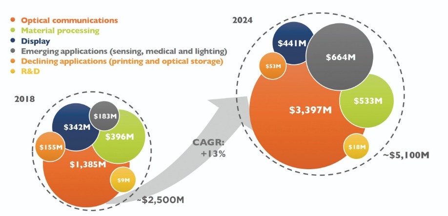
Caption: Rising revenues for edge-emitting lasers. Source: Edge-emitting Lasers – Market and Technology Trends 2019 report, Yole Développement, 2018)
With its latest funds, Ascatron is ready to scale production of high-voltage SiC devices to meet growing market demands, reports Rebecca Pool.
In July this year, Sweden-based SiC power semiconductor developer, Ascatron, revealed it had raised Ä3.5 million in funds, following the sale of shares in Basic Semiconductor, a joint venture business in China.
Now focusing on product development and volume production, the company is currently providing its first devices – 1200 V and 1700 V diodes - to customers for design-in projects, with MOSFETs scheduled for volume production next year.
“Right now we are working on 1200 V devices and higher,” says Ascatron chief executive, Christian Vieider. “We see our competitors having difficulties getting out products with higher voltages than 1700 V so high-voltage devices are our focus.”
“Our next step is to increase capacity, and we will coordinate this in line with customer demand,” he adds. “We have good connections with suppliers of epitaxy equipment and we see this as being feasible within a one-year time period.”

Ascatron Chief Executive, Christian Vieider
Critical technology
Ascatron span out of Swedish research institute, Acreo, in 2011, and has since developed myriad processes for manufacturing SiC semiconductors. They include substrate buffers, SiC epitaxy, deep trench etching and more.
At the heart of its processes lies the company’s proprietary technology, ‘3DSiC’, that is based on embedded epitaxial growth methods that replace the conventional process of doping with ion implantation during fabrication.
Doped material is grown over 3D structures, such as trenches and doped patterns, reducing electric fields at Schottky contacts and MOS interfaces and boosting device performance. For example, Ascatron claims losses can be reduced by up to 30 percent compared to devices fabricated via conventional processes.
Crucially, the company has spent the past year transferring the process from its in-house clean room at the Electrum Laboratory, just outside Stockholm, to an external foundry. According to Vieider, Ascatron’s design is now cost-compatible with competitors, and the company is currently gearing up for volume production.
“We use this buried grid in our design to shield off electric fields and then fabricate the Schottky diode or MOSFET on top of this,” says Vieider. “This was a new process step for the foundry, but we’ve got this to work and we are now getting the same results at the foundry as in our own clean room, which is a big achievement for us.”
Up until now, Ascatron has been manufacturing some 1000 epiwafers a year on its own equipment, but Vieider is keen to triple production in the short term, and take volumes to at least 1000 a month in the next three to four years. As he points out, the foundry capacity is more than 20,000 wafers a year, although, in his words: “It could take some time for us to get to this level [of production] from where we are now.”
And as a handful of SiC device makers have been making the tricky transition from 100 mm to 150 mm wafers, grappling with yields and defect levels, Vieider anticipates Ascatron production will be centred on the 150 mm size for the foreseeable future. “Six-inch wafers are still not as high quality as four-inch wafers. So in terms of quality, we would be stepping back a couple of years by shifting to eight-inch wafers, even if these were available to buy,” he says.
But could industry issues over SiC wafer supply stymie Ascatron’s plans for volume production? Vieider isn’t worried.
“Everyone is fighting these wafer shortages but we haven’t seen any problems yet,” he says. “For us volume production starts at 1000 wafers a month and from what we understand these volumes are available.”
“Also, if we talk about scaling over a two-year period, our suppliers don’t anticipate this being a problem as they are investing heavily in capacity,” he adds.
So what now for Ascatron? With its fabrication process qualified, the company is working on product qualification, which Vieider reckons will be achieved towards the end of 2020. The company is targeting high-power, high-voltage applications, including industrial and the all-important electric vehicles, and its focus will remain firmly here.
“We have seen interest in 650 V devices but right now we need to focus on our buried-grid technology and there is a clear advantage for this at the higher voltages,” says Vieider. “Also, it’s important for us to be competitive with other silicon carbide vendors by having a design where we can increase the current density and make our chips smaller, so we can get more chips on every wafer.”
And importantly, Vieider is confident that Ascatron is ready to compete with the likes of Infineon and Cree. “From customer feedback, Infineon is the reference, so we have been evaluating our first products against its high-performing devices,” he says. “We have our innovative design which gives us many advantages compared to these bigger companies.”
At the same time, Ascatron can also tailor its diode design to customer requirements. “Until recently, we were considering packaging but we’ve now reduced our product offering to bare dies so that our customers take care of the packaging and offer a complete module,” he says. “In this way Infineon could also be our customer.”
Widely used in silicon fabs, the corona non-contact C-V technique is now available for wide bandgap semiconductors
BY MARSHALL WILSON FROM SEMILAB SDI
Material AND DEVICE characterisation is an essential step in the production of compound semiconductor devices. To carry this out, foundries and chip manufacturers have dedicated metrology tools that offer a wide variety of characterisation techniques. One of these key techniques is capacitance-voltage (C-V), which provides important information such as dopant concentration, as well as dielectric and interfacial properties.
Standard C-V measurements are well-established, but have significant drawbacks. There is a cost associated with fabricating electrical test structures, and feedback can take weeks. When devices are being developed, this slows progress; and when C-V is used to monitor a manufacturing process, it takes longer for issues to be identified, compromising yield. An additional downside with standard C-V is that it is a destructive test, preventing the use of monitor wafers in subsequent production. To address these issues, the industry needs a non-destructive, cost-effective form of C-V metrology that provides rapid feedback for device development and manufacturing process control.
Fulfilling all of these requirements is advanced corona-based non-contact C-V (CnCV) metrology, developed for comprehensive C-V characterisation of wide bandgap semiconductors, dielectrics and interfaces. It offers a non-destructive, preparation-free alternative to standard C-V that trims manufacturing costs, while slashing the time for data feedback from weeks to just minutes.
CnCV is based on the corona-Kelvin technique that is not new. It is a proven, production-tested method that has been widely adopted in silicon fabs since the 1990s. More than 400 of these tools have been installed worldwide, used primarily for dielectric characterisation. Recently, however, the use of this technique has expanded, so that it can start to serve the wide bandgap power and RF industries through characterisation of SiC, GaN and Ga2O3 based materials.
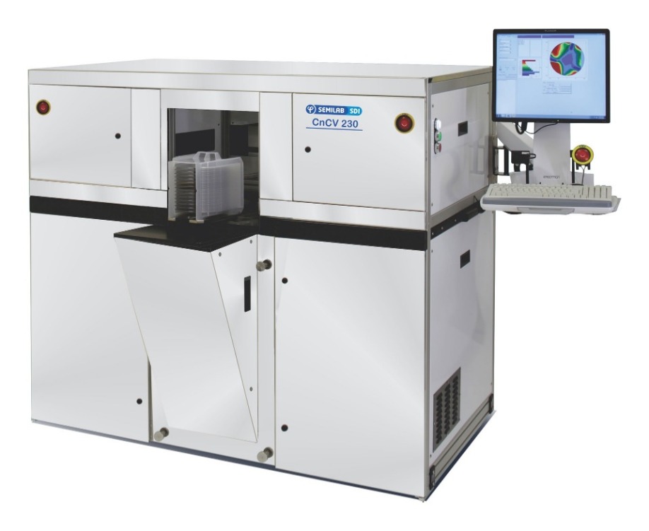
Semilab SDI CnCV 230 tool for non-contact C-V characterisation of wide bandgap semiconductors.
To control the semiconductor manufacturing process, engineers must map the wafer surface. This enables them to evaluate process uniformity and identify localised defects. Our tool helps them in this endeavour – all of the parameters that are listed in Table 1 can be measured very precisely, at selected locations on a wafer, with results displayed as contour maps that reveal process uniformity.
Principles of CnCV
In CnCV metrology, electric charge that is needed for bias is provided by corona discharge in air. These charges– they may be positive or negative, depending on the selected discharge polarity – are gently deposited on the surface of the wide bandgap semiconductor or dielectric in known charging increments. These charge increments induce a change in surface voltage, which is measured in a non-contact manner, using a vibrating Kelvin probe (see Figure 1). The non-contact capacitance is calculated by dividing the change in charge by the change in voltage. In a corona charge bias sweep, the semiconductor space charge and the surface barrier are cycled between accumulation and depletion. By adopting this approach, the technique provides a full set of data including voltage, charge, capacitance and surface barrier voltage, as well as plots of V-Q, C-Q and C-V. These characteristics form a basis for quantification of the semiconductor, interface and dielectric parameters. Armed with all this information, engineers can gain great insight into the nature of their wide bandgap material and devices.
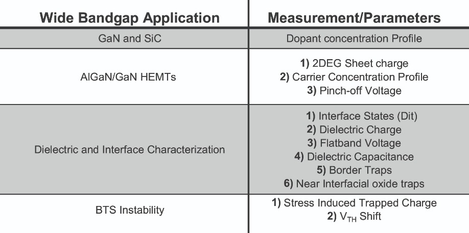
Table 1. Applications of the CnCV technique to wide bandgap materials.
Characterising promising power devices
One of the wide bandgap power devices that is growing in revenue, and will continue to do so, is the SiC MOSFET. Its attributes include delivering great performance at high fields and high temperatures, but operating in this manner makes the device susceptible to bias- and temperature-induced instability of the threshold voltage. Variations in the threshold voltage stem from complex interfacial instability phenomena, such as near-interfacial oxide trap charging.
To characterise the interfacial properties of dielectrics on wide bandgap semiconductors, engineers now have the CnCV technique at their disposal. It offers a quick assessment of threshold voltage changes before and after bias and thermal stress. This feedback aids investigations of process changes that aim to mitigate this instability, and ultimately improve device reliability.
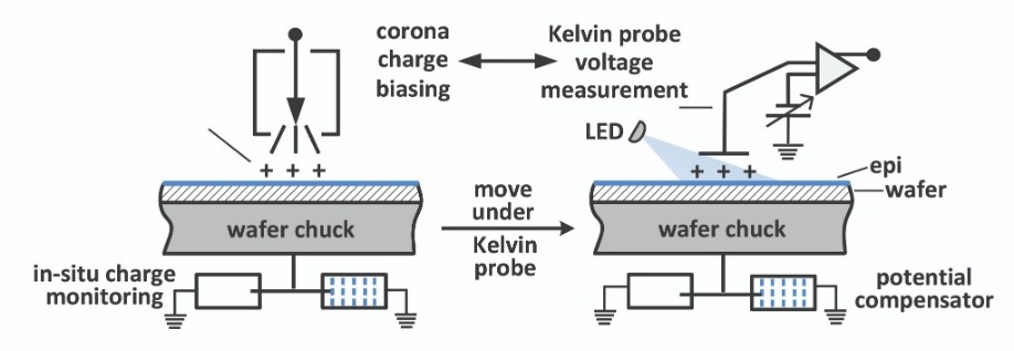
Figure 1. The basic operation of the CnCV technique.
New developments
Recently, there have been several valuable developments in CnCV metrology, enhancing its appeal for the characterisation of wide bandgap semiconductors, dielectrics and interfaces. These new features are focused on characterising aspects of material properties that are critical for wide bandgap device performance and reliability.
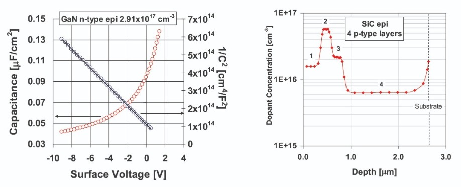
Figure 2. Non-contact corona based CnCV can be used to characterise epitaxial SiC and GaN layers, providing plots of C-V and 1/C2 characteristics (example of n-type GaN on the left). CnCV can also measure dopant profiles on multiple layer epi samples (example of four-layer SiC epi on the right).
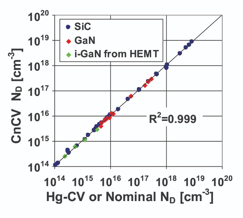
Figure 3. There is a high degree of correlation between CnCV and standard mercury C-V results of dopant measurements on epitaxial SiC, GaN and intrinsic GaN in HEMT structures.
It is very valuable to determine an accurate value for the flatband voltage, which serves as an anchor point allowing the determination of the oxide voltage and the surface barrier, at any given charge (see V-Q plot in Figure 5, top). The capacitance-voltage and capacitance-charge (see Figure 5, bottom) characteristics are then calculated.
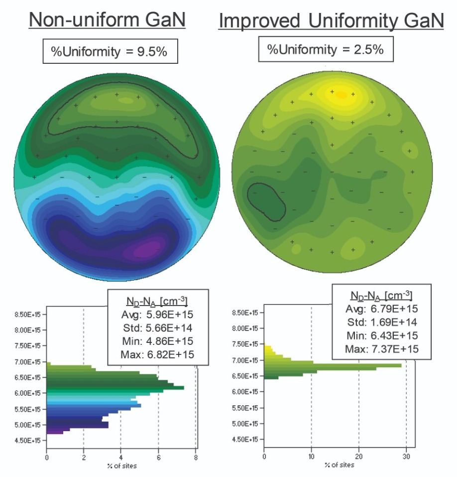
Figure 4. CnCV maps of net dopant concentration on silicon-doped, n-type GaN MOCVD epilayers on GaN substrates show the benefit of process improvement, which reduces the non-uniformity of compensating acceptors.
A key feature of materials with a wide bandgap is a large energy separation between the interfacial traps and the edges of conduction and valence bands. Due to this, deep traps cannot maintain occupancy dictated by Fermi statistics, and they remain largely invisible in dark C-V sweeps. Take oxidised n-type SiC, and carry out a sweep that stretches from accumulation to deep depletion, and only shallow interface traps will empty themselves when they move above the Fermi level. Consequently, measurements of interface trap density spectra are limited to about 0.7 eV below the conduction band – that’s less than a quarter of the energy gap. This is a significant impediment, as deep states, uncovered by photo-assisted C-V and current measurements, are known to impact device performance.
To address this concern, we have applied a form of photo-assisted C-V characterisation to our CnCV technique. This addition allows engineers to characterise deep interface states very quickly. We have also adopted the surface photovoltage spectroscopy method, invented back in the 1960s at MIT. This uses a monochromatic source of light with sub-bandgap energy to provide further insight into properties of these deep states.
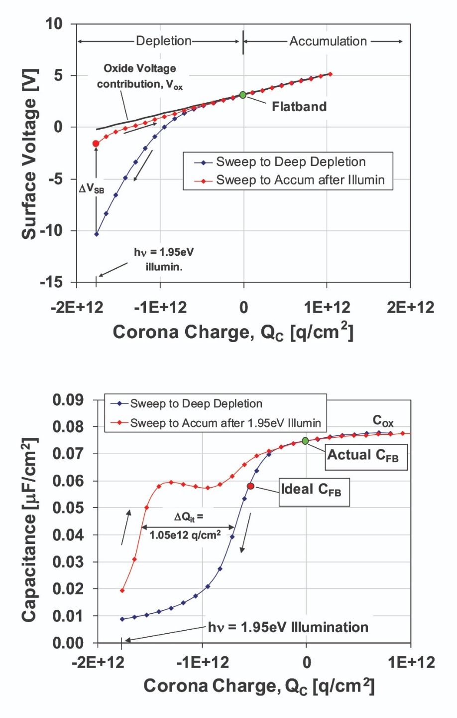
Figure 5. CnCV V-Q (top) and C-Q (bottom) characteristics on n-type SiC with a 45 nm-thick insulating layer of SiO2. Illumination causes photoionisation of interface traps and a negative shift in C-Q characteristic (bottom).
We can see the effect of photoionisation in our V-Q and C-Q plots (see Figure 5). Emptying traps decreases the surface barrier, but does not affect the oxide voltage or corona charge. Photons with an energy above the photoionisation threshold depopulate the deep interfacial traps. When the density of trapped interfacial electrons falls, this is manifested as a surface voltage transient (see Figure 6).
With this approach, the magnitude of the change in photoionisation-induced surface voltage gives a measure of the deep interface state concentration. Recording the time constant of the photoionisation decay, using a constant illumination intensity and wavelength, identifies the specific interfacial trap involved in the process – in analogy to the thermal emission constant in deep-level transient spectroscopy.
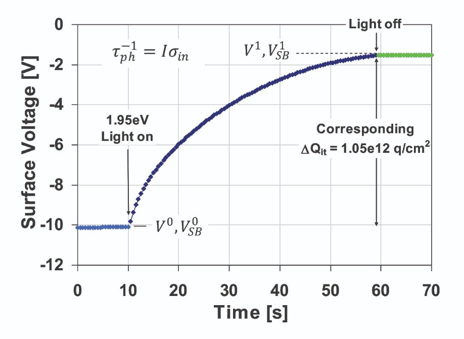
Figure 6. Surface-voltage transients corresponding to Figure 5, resulting from photoionisation of deep interface traps with 1.95 eV illumination.
Illustrating the power of the CnCV technique are measurements made on oxidised SiC, before and after a 850 °C, 8 hour, wet annealing process. Rapid feedback CnCV provides plots of C-Q before and after photoionisation revealing a reduction in deep interfacial states (see Figure 7, top) and shallow interface states (see Figure 7, bottom) by more than a factor of two. This indicates that annealing reduces various types of interface states that are known to cause flatband voltage instability under bias stress conditions. The ability to obtain such quick feedback about the impact of various stages of processing on parameters important for device fabrication can help to greatly improve cost and time savings in process development.
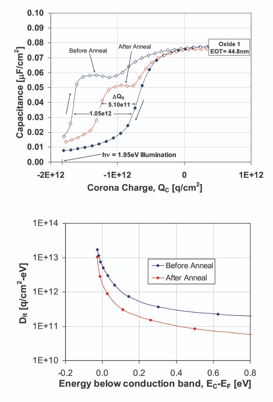
Figure 7. Photoionisation of deep interfacial states using sub-bandgap illumination enables their characterisation using unique photo-assisted CnCV C-Q curves. Example shows reduction in deep (top) and shallow (bottom) interface states before and after a wet post-oxidation anneal.
With sales of wide bandgap power devices rising throughout the next few years and beyond, there will be a growing need for characterising the electrical properties of SiC, GaN and Ga2O3. We have no doubt that the best way to meet this demand is with CnCV, a powerful and convenient non-contact, non-destructive alternative to standard C-V and mercury C-V. CnCV has the upper hand on many fronts: it saves time; it cuts costs; and it offers many unique insights that are not possible with standard C-V, such as direct determination of the flatband voltage and C-Q characteristics. Such attributes will help those that are developing wide bandgap devices, and also those that are ramping production to keep pace with demand.
M. Wilson et al. ECS J. Solid State Sci. Technol. 6 S3129-S3140 (2017)
A. Savtchouk et al. Materials Science Forum 509 858 (2016)
The roll-out of 5G is going to benefit the compound semiconductor industry. Volumes of GaAs HBTs and GaN HEMTs are set to flourish, and a ramp in other technologies could follow, such as that of the GaAs pHEMT and the GaN-on-silicon transistor
BY RICHARD STEVENSON
There are some people that always want the latest and the best. They are sure to be ones to splash out on a 5G smartphone, allured by the promise of a faster connection that could enable a 4K movie to be downloaded in a minute or so.
It is likely that these early adopters will be heavily disappointed. If they live in a city that has just rolled out 5G, it is true that they will enjoy better connectivity – and when everyone wants to access the internet at the same time, that’s highly valued. But if they expect to download data at breath-taking speeds, they will probably be in for a shock. According to many experts, the increase in speed will be only about 20 percent.
Why are these expectations going to be so different from reality? Well, it’s because 5G is being deployed in two phases – and it is only the second phase, which doesn’t start rolling out until around 2023 at the very earliest, that is going to deliver a substantial hike in data rates, thanks to a move to wider frequency bands in the millimetre-wave spectrum above 24 GHz.
Right now, it is only the roll-out of a sub 6 GHz band that is underway. This typically operates at a frequency of 2.6 GHz or more, and as well as increasing coverage for subscribers, it will open up new business opportunities for operators, such as industrial monitoring.
Only by understanding the details of this two-phase deployment, as the analysts at Yole Développement do, is it possible to predict how the emergence of 5G will impact sales of RF compound semiconductor devices. According to experts at Yole, the roll-out of 5G will be good for GaAs and GaN. Production of GaAs-based power amplifiers for mobile phones will increase, as the introduction of the new network will lead to, on average, an additional amplifier in every phone; and sales of GaN HEMTs will rise as carriers deploy 5G infrastructure, which will start forming national networks in the next few years.
In cities in South Korea, the UK, the US, Japan and China, deployment of a 5G, sub 6 GHz network is already underway.
“The technology looks a lot like LTE,” says Antoine Bonnabel, Technology & Market Analyst for the Power & Wireless team at Yole. Thanks to this similarity, Bonnabel argues that it is relatively easy to develop and implement this form of 5G, with existing base stations upgraded to include this new communication technology.
In some dense urban areas, operators are improving their coverage by also introducing a network of small cells. This has happened in South Korea, where Samsung has deployed 53,000 of them, operating at 3.5 GHz. Operators are using these cells to initially provide LTE coverage, but in time they will be upgraded to operate on the 5G network.
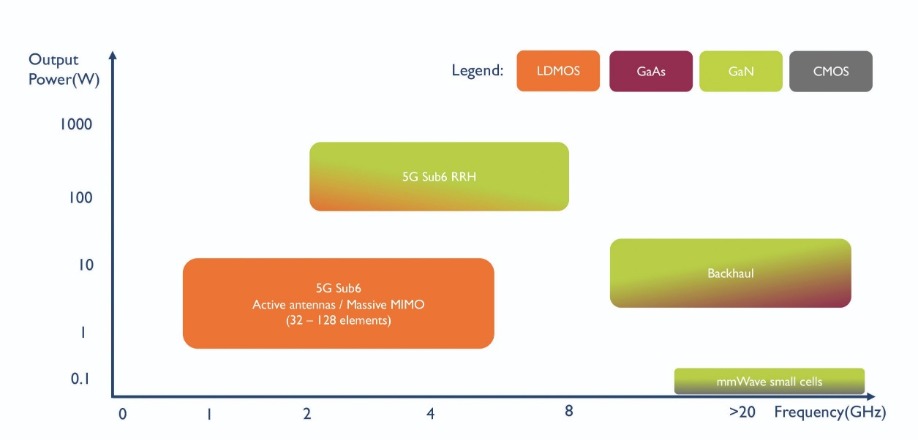
Today, the two most common technologies for wireless communication are silicon LDMOS and GaN, with the latter having the upper hand at higher frequencies. Taken from 5G Impact on Telecom Infrastructure report, Yole Développement, 2019.
The output of these small cells is less than that of conventional base stations. Rather than producing 240 W, it’s typically between 40 W and 80 W. “It’s still high power,’ says Bonnabel. “You can reach up to a few hundred metres.”
GaN versus silicon
For many years, network operators had to choose between silicon LDMOS and GaN to provide the amplification in the base station. For the emerging 5G networks, the base station needs to deliver a high-power at a relatively high efficiency, a requirement that plays into the hands of GaN. According to Bonnabel, for all the 5G base stations built with conventional technology, as frequencies are above 2.6 GHz, GaN is the only viable option.
As carriers have moved from one generation of communication technology to another, they have also, independently, advanced their antennae technologies. One innovation has been the introduction of active antennae, a move that allows beam-forming and massive MIMO. To deliver these technologies, a small front-end is employed at each antenna, rather than a single front-end for all antenna elements. Configuring the base station in this manner slashes the power requirement for each antenna element, opening the door to the use of silicon LDMOS in 5G networks.
However, even though GaN faces competition from silicon LDMOS for some tasks within the 5G network, shipments of this device will still rise fast. According to Bonnabel, sales of GaN devices to the base station market will increase from $300 million this year to $750 million by 2024.
Bonnabel says that today, the only substrate used for the production of these GaN HEMTs is SiC. However, he points out that the opportunity to turn to a silicon substrate has attracted much interest within industry, due to its potential for low cost, with prices approaching those of silicon LDMOS.
Grabbing the lion’s share of the GaN-on-SiC market is the Japanese firm Sumitomo, which ships its GaN amplifiers in the form of discrete devices. “The main reason [for their dominance] is that they are the exclusive supplier of Huawei,” says Bonnabel, who believes that Sumitomo’s success is deserved, because it has the best technology – and it continues to refine it. To cater to the growing market, Sumitomo is increasing its production capacity, a move that will help it to stay ahead of a chasing pack that includes Wolfspeed and Qorvo. Legislation in several countries, related to security concerns, has dented Huawei’s attempts to win contracts to deploy 5G all over the world.
“China, because of this ban, has invested more in its 5G deployment than it was supposed to,” says Bonnabel. “The investment that they were supposed to make over the course of three years, they have made it in a year.”
One advantage that Huawei has over its peers in the 5G market is that it has a lot of expertise in making and deploying devices operating at relatively high-frequencies within the sub 6 GHz band. In comparison, the main frequencies in today’s networks in the US and Europe are below 2.6 GHz, a domain well served by Nokia and Ericson.
Ironically, it is only recently that the US has permitted the use of higher frequency bands, such as those at 3.5 GHz and 4.2 GHz. In developing countries, legislators are far more willing to permit the use of higher frequencies, and operators are using them for 4G deployments. “They go for Huawei products, because they are 30 percent cheaper than Ericson,” says Bonnabel.
5G smartphones
Alongside the roll out of 5G networks is the introduction of a handful of compatible smartphones. Aside from a couple of exceptions, 5G capability is limited to the sub 6 GHz network.
So far, 5G smartphone sales have totalled between 5 million and 10 million, according to Cédric Malaquin, a Technology & Market Analyst who specialises in RF devices & technologies and works within the Power & Wireless division at Yole. Malaquin expects that even by the end of this year, sales of 5G phones will not have exceeded 50 million, and it will take until 2025 before they can account for 30 percent of the market. “So, in number, something like 600 million units.”
The compound semiconductor content in the smartphone is in the form of a GaAs power amplifier. “The power and efficiency is unmatched by any other technology, especially CMOS,” says Malaquin. He expects the dominance of the GaAs power amplifier to continue, as operators are requesting more and more power from the device to the base station.
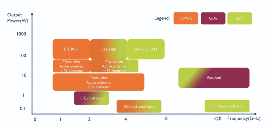
By 2025, GaN will be the dominant technology in traditional base stations, and in millimetre-wave 5G. However, in massive MIMO, silicon LDMOS is tipped for success. Taken from 5G Impact on Telecom Infrastructure report, Yole Développement, 2019.
Rivals in this sector include Skyworks, Murata and Qorvo – an entity formed from the merger of RFMD and TriQuint – that are drawing on their in-house GaAs power amplifier technology to make front-end modules. Up against them are the likes of Qualcomm and Broadcom, all making their own GaAs power amplifiers by drawing on the services of GaAs foundries, such as WIN Semiconductors of Taiwan.
It is not easy to assess the impact of the introduction of sub 6 GHz 5G networks on the production volumes of GaAs power amplifiers. In some countries, such as Japan, the established 4G networks operate at high frequencies, and it is possible that a design engineer could use one amplifier for both the 4G and 5G signals. But that is not the norm, according to Malaquin, who has calculated that, on average, the introduction of 5G will lead to the addition of one power amplifier per phone. That’s good news for the makers of MOCVD tools, GaAs substrates, metal-organics sources and characterisation equipment, that will all welcome the additional business.
Note that the key component in the front-end module is not the GaAs power amplifier, as its production can be outsourced. “It’s more important to have the right cost and the right performance for the filter,” says Malaquin, who argues that it is the excellence in this technology that is behind the success of Skyworks, Qorvo, Broadcom, Murata and Qualcomm.
Millimetre-wave networks...
The second phase the 5G rollout – the introduction of a millimetre-wave network – will require a revolution, rather than just an evolution, in infrastructure. At frequencies of 24 GHz and above, signal attenuation is far higher, so the smartphone must be far closer to the base-station. Consequently, there needs to be a far denser network, which will be made of small cells. Deploying this only makes sense in areas where there are large crowds, such as sports stadia.
Trials of millimetre-wave networks are underway. In the US, there has been great interest in this technology, but according to Bonnabel, those working in this area have found it more challenging than expected. “Right now there is a move back from millimetre wave, and larger interest in sub 6 GHz frequencies.”
Bonnabel believes that it will be 2023 before the millimetre-wave market starts to develop, and from then on growth will be modest. “Operators spend a limited amount of money on their annual deployment, so the amount of money for millimetre-wave small cells will be limited, and will not grow,” reasons Bonnabel. He expects a saturation in sales to the small cell market to occur by 2025. “We don’t expect it to be a booming market that will see millions and millions of devices.”
It is not yet clear what technology will be used in these small cell deployments. In today’s trials, millimetre-wave cells employ GaN. “In the longer term, when you reach a large number of antenna per small cell, you may not choose a power amplifier, and you might be able to use CMOS itself,” argues Bonnabel.
…and smartphones
For those living or working where 5G millimetre-wave trials are taking place, there is the opportunity to experience this revolutionary network by buying one of a very small number of compatible handsets. They include a version of the Samsung SG105G, and a solution from Motorola. It far from easy to cram the additional technology into a phone that enables it to operate in the millimetre-wave band. In fact, Motorola doesn’t even try, preferring instead to have a separate unit for this spectral domain, and strapping it onto one of its Z-Series phones (see the image on the right).
Designing a handset that works well at these frequencies is a tough ask. Antenna gain is low, and current CMOS power amplifiers are inefficient. “It’s a problem for your battery life,” says Malaquin.

The 5G Moto Mod, which provides millimetre-wave connectivity, places a 5G modem inside a plastic backpack. Using magnets and pogo pins, this unit bonds to a Motorola Z-series phone.
Over the next few years, other technologies could come to the fore. “Above 6 GHz, your HBT today doesn’t do the job,” says Malaquin. “But the pHEMT, it’s a different story – you can use the pHEMT design to do a millimetre-wave power amplifier.” Another candidate is GaN-on-silicon, a technology dogged by concerns over reliability.
This is further evidence that there is much uncertainty surrounding the revolutionary phase of 5G. That’s certainly not the case for the first phase, which is an evolution of 4G LTE that will drive an increase in the production of GaAs HBTs and GaN HEMTs. So, in the short term, 5G is definitely going to be good for the compound semiconductor industry – and looking further ahead, there could be additional sales from the roll out of millimetre-wave networks.
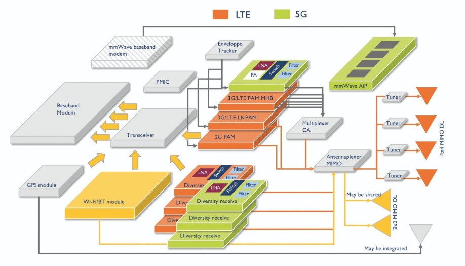
The introduction of 5G will have an impact on the architecture of the RF front-end of mobile devices. Taken from 5G’s Impact on RF Front-End Module and Connectivity for Cell phones report, Yole Développement, 2019.
Record-breaking modulation speed are realised at elevated temperatures by fabricating VCSELs with two apertures, formed by zinc-diffusion and oxide relief
BY JIN-WEI SHI FROM NATIONAL CENTRAL UNIVERSITY, TAIWAN
Demands on data centres are rocketing. That’s no surprise, given the rise of Netflix, Youtube, social media, and far greater use of the cloud.
To cope with this ever-increasing demand, there have been changes taking place within the infrastructure of the data centre. Historically, coaxial cables have routed data between different central processing units and different mother boards. But these cables are bulky, lossy, and highly dispersive – and they fail to accommodate the tremendous increases in both the data rate and the number of channels in the data centre. So, to overcome this bottleneck associated with the total bandwidth capacity in the data centres, coaxial cables have been replaced with optical fibres. They have the upper hand on many fronts, combining a far lower loss with less dispersion, a broader bandwidth and a smaller form factor. The only downside is that by moving from the electrical to the optical domain for the links, additional electrical-to-optical and optical-to-electrical processes have to be inserted on the transmitting and receiving sides of fibre, respectively.
One option for the light source that generates the data for the optical link is the edge-emitting, distributed feedback (DFB) laser. It is a well-established device, deployed in the traditional optical communication network, where the length of the fibre can be up to thousands of kilometres. The DFB laser dominates this application, because of its high optical output power, low chirp, and a narrow spectral width, a set of attributes that make it ideal for transmitting data over vast distances with very low error rates. But the DFB laser is not a good option in datacentres, where many millions of high-speed light sources have to be densely packaged with ICs, to move data at high speeds between different boards and chips. Its Achilles heel is its relatively high power consumption, which can lead to thermal management issues, wasted heat, and a high carbon footprint for the data centre.
For this particular application, a far better candidate is the VCSEL. In data centres, over 95 percent of fibre channels have linking distances less than 50 metres, so fibre loss and dispersion are not major concerns. In these very-short-reach links, what is paramount is to minimise the electrical-to-optical and the optical-to-electrical conversion losses. And when judged in this manner, the VCSEL wins hands down, consuming just one-tenth of the power of the edge-emitter, thanks to the far smaller size of the optical cavity.
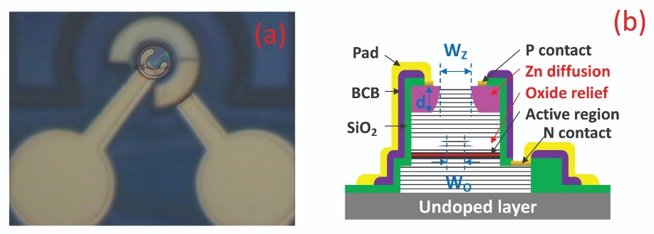
Figure 1. By turning to a double-aperture design, researchers at the National Central University, Taiwan, have set a new benchmark for VCSEL performance. (a) Top-view and (b) conceptual cross-sectional view of the demonstrated device.
Working at the National Central University, Taiwan, our team has developed a novel form of VCSEL that sets a new benchmark for performance. This device, a prime candidate for serving tomorrow’s datacentres, features a pair of apertures (see Figure 1). One is defined by zinc diffusion, and allows us to manipulate the number of modes of the VCSEL; and the other is created by oxide relief, and provides us with a lever for the device modulation speed.
A great strength of our device is that it is able to deliver a record-breaking performance at elevated temperatures. For those that build data centres, this is a very valuable attribute. When VCSELs are paired with photodiodes to form transceiver modules, they must be packaged as close as possible to the electronic integrated circuits, which generate a significant amount of heat during high-speed operation. Dense packaging is essential, because it minimises propagation loss and dispersion in the high-speed electrical signals transmitted by the printed circuit board. However, heat generated by the ICs increases the junction temperature of the VCSEL, applying the brakes to the modulation speed.
To serve in the next generation of optical interconnect channels, VCSELs need to have a high-speed performance that is almost invariant with temperature. A data rate of more than 50 Gbit/sec per lane must be maintained between room-temperature and over 85 °C.
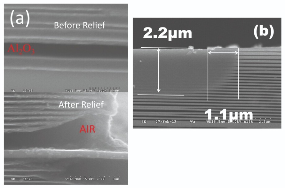
Figure 2. (a) Scanning electron microscopy image of the DBR structure withthe oxide current-confined layer before and after performing an oxide relief process. (b) Scanning electron microscopy image of DBR layers after the zinc-diffusion process.
Armed with this form of active region, our novel design of 940 nm VCSEL has realised record modulation bandwidths. Judged in terms of optical-to electrical conversion, for a -3dB loss, we have recorded bandwidths of 40 GHz and 32 GHz under room-temperature and at 85 °C. These milestones follow important successes by other groups, such as: a team led by researchers Chalmers University of Technology that reported a 850 nm VCSEL with a 3 dB electrical-to-optical bandwidth of 30 GHz in 2015; and in the same year, a group at the University of Illinois, Urbana Champaign, that announced a multi-electrode VCSEL with a 3 dB bandwidth up to 37 GHz. Recently, the company VI System demonstrated single-mode VCSEL chips with 3 dB bandwidth up to 30 GHz.
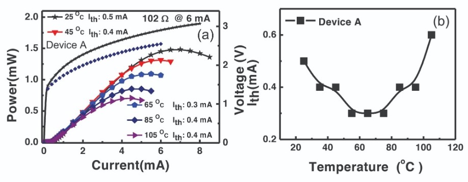
Figure 3.
(a) Measured power-current-voltage curves under different ambient temperatures; (b) corresponding threshold current (Ith) versus ambient temperature.
(b) Figure 4. Bias dependent electrical-optical frequency responses under (a) room-temperature and (b) 85 °C operation. The corresponding bias-dependent output optical spectra under (c) room-temperature and (d) 85 °C operation.
(c) Figure 5. The measured (a) 50 Gbit/s at room temperature, (b) 50 Gbit/s at 85 °C, and (c) 60 Gbit/s at room temperature OOK transmission eye-patterns over 1 m OM5 fibre (back-to-back) without signal processing; (d) corresponding bathtub curves. The bias current and peak-to-peak driving voltage (Vpp) applied to the device during measurement are 5 mA and 0.55 Vpp, respectively
We fabricate our VCSELs by processing epiwafers purchased from Landmark. Grown on an semi-insulating GaAs substrate, our epiwafers feature: an active region with several InGaAs quantum wells; an aluminium-rich AlGaAs oxidation layer that sits just above the active region; and a pair AlGaAs-based distributed Bragg reflectors, which form the mirrors either side of the active region (see Figure 1).
Our first step is to process these epiwafers into mesa structures with diameters of typically 30 µm. After this, we employ wet oxidation and oxide-relief processes to selectively remove the AlxO1-x current confined layer. During these two processes, oxidation takes place in the oxide current-confined layer and also at the edge of distributed Bragg reflector layers with high aluminium concentrations. Consequently, both are subsequently etched away (see Figure 2 (a), which shows scanning electron microscopy images of our oxide aperture before and after the oxide relief process).
The oxide-relief process is beneficial. As the refractive index of air is much smaller than that of the AlxO1-x layer – it is 1, rather than 1.6 – there is a further reduction in the parasitic capacitance of the oxide-relief device. This leads to an increase in the bandwidth of the VCSEL, so that it can operate at a higher data-rate.
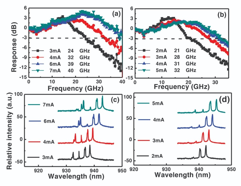
Figure 4. Bias dependent electrical-optical frequency responses under (a) room-temperature and (b) 85 °C operation. The corresponding bias-dependent output optical spectra under (c) room-temperature and (d) 85 °C operation.
In a typical VCSEL, there is just one aperture, formed by oxidation. But in our devices, we have a second one, created by zinc-diffusion. A downside of the diffusion process is that it supresses the local lasing phenomenon: threshold gain increases in the zinc-diffused region, due to a rise in free-carrier absorption loss; and there is also a reduction in reflectivity. However, there is an upside too, as zinc diffusion enables mode control, a key to improving the quality of data transmission through an optical fibre. Improving mode control trims chromatic dispersion, and in turn increases the transmission distance, which can be valuable in modern data centres that have expanded to several buildings to accommodate the demand for more data, and may contain links of a kilometre or more.
We use a high-quality Si3N4 layer to create a diffusion mask that controls the location of the zinc within our device. Inspecting the distributed Bragg reflector after the diffusion process shows that it introduces a great deal of disorder – the individual layers are no longer visible with a scanning electron microscope (see Figure 2 (b)). This disordering is beneficial, as it reduces the contact resistance when the injected current flows through the distributed Bragg reflector.
To evaluate the performance of our VCSELs, we have plotted their current-voltage-light characteristics and their threshold current over temperatures ranging from ambient to 105 °C (see Figure 3). These measurements show that over that temperature range the increase in the threshold current is very small – it is less than 0.2 mA. We attribute this to the large conduction band offset in the AlGaAs/InGaAs active region, which minimizes electron leakage.
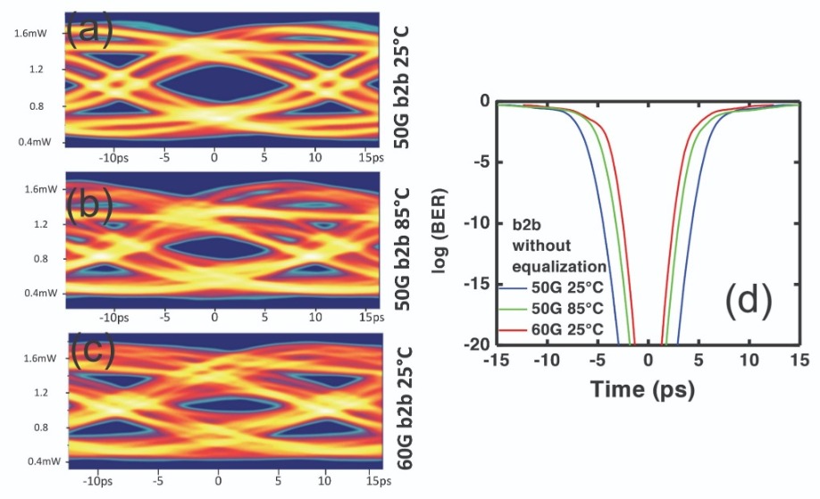
Figure 5. The measured (a) 50 Gbit/s at room temperature, (b) 50 Gbit/s at 85 °C, and (c) 60 Gbit/s at room temperature OOK transmission eye-patterns over 1 m OM5 fibre (back-to-back) without signal processing; (d) corresponding bathtub curves. The bias current and peak-to-peak driving voltage (Vpp) applied to the device during measurement are 5 mA and 0.55 Vpp, respectively
Another attribute of our VCSELs, highlighted in Figure 3, is their low differential resistance. Under a 6 mA bias current, differential resistance is as low as 100 Ω at room temperature, and just 80 Ω at 85 °C. In comparison, conventional 980 nm VCSELs with a similar size of oxide aperture – that is, about 3 mm – have differential resistances of typically 200 Ω at 85 °C. The superiority of our devices stems from the zinc-diffusion process and the topmost current-spreading layers.
We have also measured the bias-dependent electrical-optical frequency responses of our VCSELs, and their corresponding output optical spectra, at both room temperature and 85 °C (see Figure 4). The graphs show that the maximum 3 dB electrical-optical bandwidth can hit 40 GHz at room-temperature, and is still as high as 32 GHz at 85 °C.
Additional measurements have been made to evaluate the capability of our VCSELs to transmit data through a fibre. They include 50 Gbit/s and 60 Gbit/s on-off keying transmission results with eye-patterns and corresponding bathtub curves for the device under room-temperature and 85 °C operation over a 1 m OM5 fibre (see Figures 5 (a) to (d)). These results are very encouraging. At 50 Gbit/s, the bit-error rate is below 1 x 10-12, all the way from room-temperature up to 85 °C, without any pre-emphasis or equalisation techniques. In other words, over this temperature range, we have produced bit-error-free transmission. What’s more, at room temperature, the maximum error-free data rate can be as high as 60 Gbit/s.
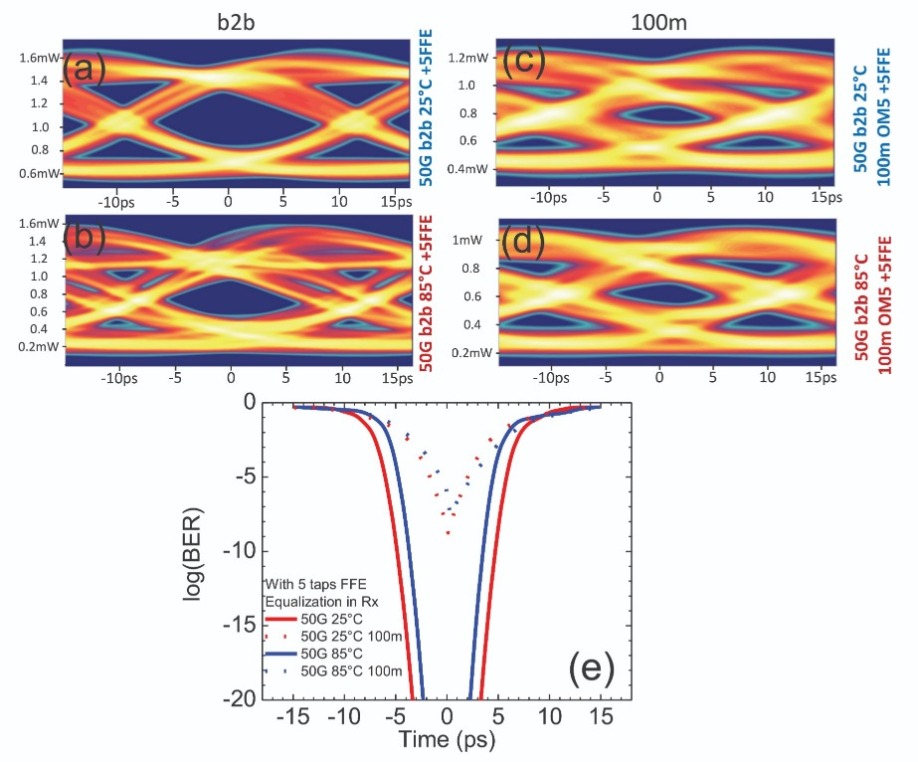
Figure 6. (a) 50 Gbit/s eye patterns measured at 25 °C and back-to-back transmission; (b) 50 Gbit/s eye patterns measured at 85 °C with back-to-back transmission; (c) 50 Gbit/s eye patterns measured at 25 °C and 100 m OM5 fiber transmission; (d) 50 Gbit/s eye patterns measured at 85 °C and 100 m OM5 fibre transmission with FFE equalization; (e) corresponding bathtub curves.
Our results are very encouraging for the future of very-short-reach optical interconnect networks. The capability of these novel VCSELs over a wide temperature range makes them very attractive candidates for data centres. In addition, they could also serve in other harsh environments. They could, for example, deliver data transmission inside autonomous cars and drones, opening up yet more markets for what is arguably the most exciting compound semiconductor device of our age.
J.W. Goodman et al. Proc. IEEE. 72 850 (1984)
D. M. Kuchta et al. IEEE Photon. Technol. Lett. 27 577 (2015)
E. Haglund et al. Electron. Lett. 51 1096 (2015)
S. T. M. Fryslie et al. IEEE Photon. Technol. Lett. 27 415 (2015)
G. Larisch et al. IEEE Photon. Technol. Lett. 28 2327 (2016)
Jin-Wei Shi et al. IEEE J. of Sel. Topics in Quantum Electronics 19 7900208 (2013)
Chen-Lung Cheng et al. Proc. OFC 2019, San Diego, CA, USA, March, 2019, W3A.2.
Near-equilibrium ammonothermal growth of multiple GaN crystals in a single vessel realises high throughout and great material quality
By Tadao Hashimoto FROM SixPoint Materials
The success of the Blu-ray player has worked wonders for our industry. It has not only given the GaN laser and its native substrate their first killer application – it has been instrumental in driving improvements in material quality. Makers of BluRay players strive for reliable products, and thus reliable lasers, so to achieve that there has been much effort directed at reducing the dislocations in the underlying GaN substrate. If it doesn’t meet the mark, it is LED-grade rather than laser-grade, and can only be used for the production of ultra-high brightness LEDs.
Twenty years on from the first commercialization of free-standing GaN wafers by HVPE, this market is now worth many tens of millions of dollars (according to market analyst Yole Développement, sales totalled $60 million in 2017). But it could be worth even more, if GaN substrates can set a new benchmark for material quality. Exceed on that front and they can underpin the development of high-power electronic and optoelectronic devices.
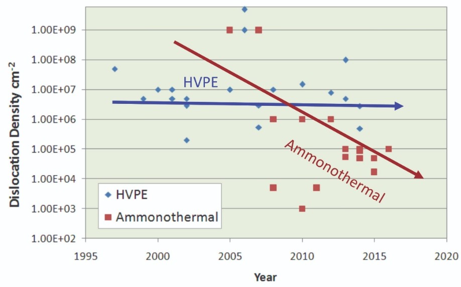
Figure 1. Historical trend of dislocation reduction in GaN.
All these efforts have been motivated by the need for high-power, high-efficiency electronic devices. More and more engineers are recognising that the best way to realise them is through a GaN-on-GaN architecture. Devices will need to combine an incredibly low leakage current in extreme reverse bias with the capability to handle a great deal of heat, to ensure reliability. Crucial to meeting these two goals are GaN substrates with a lower dislocation density than today’s laser-grade material.
Such a platform is also an essential ingredient in the production of multi-mode, high-power blue lasers. If they produce an output of 100 W or more, they can be used for machining. To produce such a source, engineers are trying to draw as much power as possible from each device within a laser array. Success hinges on handling a great deal of thermal, electrical and optical energy. For these extreme power lasers, the GaN substrates that provide their foundation must have a dislocation density that is below that found in today’s laser-grade material.
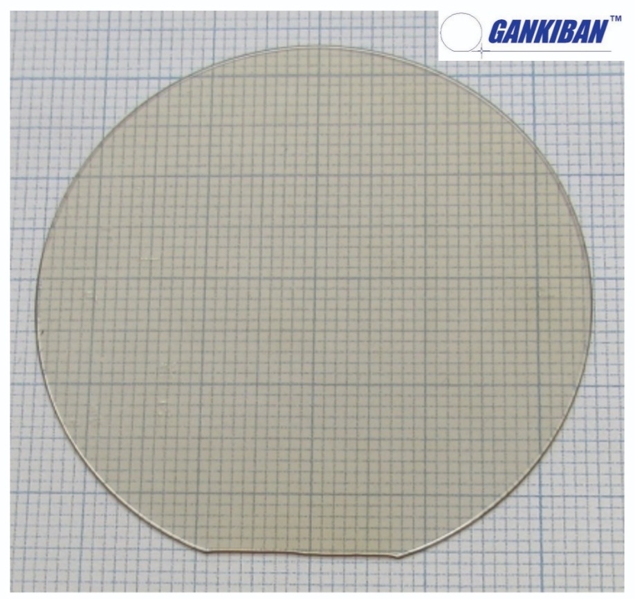
Figure 2. Near-equilibrium ammonothermal growth has been used to produced 2-inch GaN substrates.
There are two significant hurdles that must be overcome in order to enable the production of ‘power-grade’ GaN substrates with sufficient quality for the manufacture of high-power electronic devices and lasers. One is an improvement in quality, driven by a reduction in dislocation density. Progress with HVPE-grown material has stagnated over the last 15 years, with dislocation densities typically in the low-to-mid-106 cm-2; and the chances for a breakthrough are not great. Progress is held back by a lack of understanding of how to reduce defects in thick layers – those that are 100 µm or more – and the mechanism behind the generation of these imperfections. Plot the reduction in dislocations over time (see Figure 1), and results suggest that it is unlikely that there will be a significant reduction in the dislocation density in HVPE-grown material. However, there is hope, as the ammonothermal method is yielding better and better material, and further improvements are promised.
The second obstacle to power-grade material is market deadlock. Customers want more substrates at a lower price, but manufacturers can’t increase production volume without pushing up the price. Although the price of a 2-inch GaN substrate has dramatically declined over two decades, thanks to intensive, patient improvement of the HVPE process,
it appears that it cannot go any lower. Today, the leading manufacturers of GaN substrates are producing their material with fully depreciated HVPE equipment. To increase production, they would need to invest in new equipment, and recoup this outlay through an increase in the price of the substrate. So far, the producers of HVPE GaN substrates have not ventured down this road, despite increasing market demand.
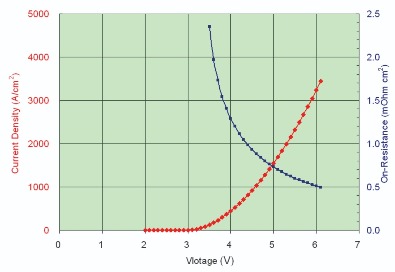
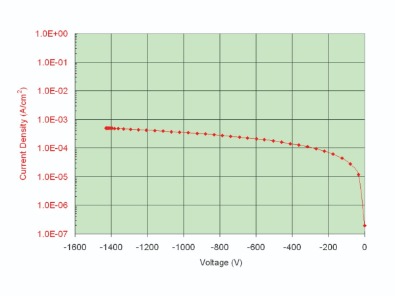
Figure 3. Current-voltage characteristics for p-i-n diodes fabricated on GaN substrates produced by near-equilibrium ammonothermal growth. Device growth, fabrication and characterization were conducted by R. Dupuis, S-C. Shen and T. Detchprohm at Georgia Tech.
At SixPoint Materials of Buellton, CA, we can overcome both of these obstacle with our near-equilibrium ammonothermal (NEAT) technology. In general, material made with ammonothermal approaches is decreasing in dislocation density year on year. For us, the typical density of our latest 2-inch substrate is low-to-mid-105 cm-2. Lower figures should follow, making our product an attractive candidate for makers of next-generation, high-power electronic and optoelectronic devices that are in search of power-grade GaN substrates.
Similar to the hydrothermal method used for the mass production of quartz, the ammonothermal technique uses supercritical fluid, which has a low viscosity and a high circulation speed. These characteristics enable a uniform temperature inside the reactor, which is a great attribute, as any non-uniformity of temperature on the growth front hampers scaling.
The ammonothermal method is renowned for its low growth rate. It typically takes an entire day to grow 100 µm, while HVPE could realise this is just an hour. Given this substantial difference, it’s no surprise that many groups have focused on increasing the speed of their ammonothermal process. Typically, this is realised by increasing the driving force of crystal growth. However, that has a downside: it results in unwanted heterogeneous nucleation inside the reactor. Once GaN nucleates, it consumes the source, leading to a drop in growth rate. Such conditions impair consistent crystal growth and deteriorate the quality of the material.
We take a different tack, growing many crystals simultaneously in a large reactor, with the growth condition near equilibrium. Using this approach, we minimise parasitic deposition, and as the crystals grow thicker, their quality improves. Although the growth rate is slow, by growing many crystals simultaneously, we compensate for this.
Thanks to the strong support of ARPA-E and DoE, we have made great progress in the development of our 2-inch GaN substrates. We refer to them as Gankiban. In Japanese, this is literally ‘GaN substrate’.
Through an intensive study of crack generation during our growth of bulk GaN, we have been able to identify the key culprits of crack generation. This insight enables us to produce 2-inch crack-free substrates (see Figure 2). They have an excellent microstructure, according to X-ray diffraction rocking curves, which have an average full-width at half-maximum of 20-70 arcsec. The dislocation density of this material, determined by defect-selective etching, is low-to-mid-105 cm-2.
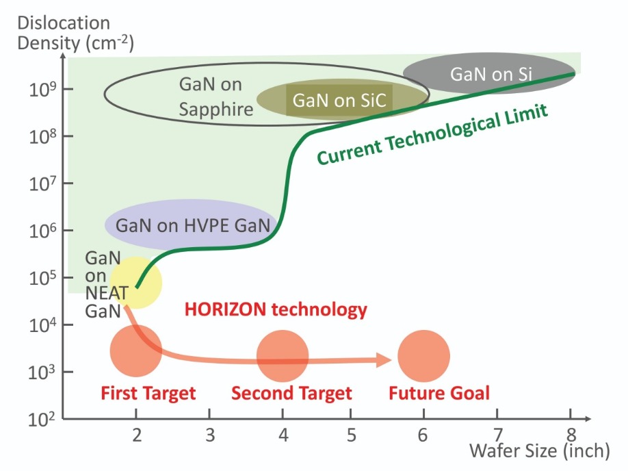
Figure 4. Current GaN technology mapped in terms of wafer size and dislocation density. HORIZON technology aims to address this dilemma and achieve low-dislocation, large-area GaN substrates.
Through our funding from the DoE, as well as optimising our ammonothermal growth process, we have been able to develop a technology for forming high-quality substrates from our crystals. Establishing a back-end wafering process is just as important as having one for crystal growth, because it is needed to make the power-grade substrates that are the bedrock for the production of high-quality epitaxial films.
We can offer this to our customers – our Gankiban substrates are epi-ready on the gallium face, and have miscut angles of 0.4°±0.1° along the m-direction and 0.0°±0.1° along the a-direction. These attributes enable the growth of high-quality GaN layers with thicknesses of 10 µm or more that will lie at the heart of high-power diodes and transistors.
Working within the ARPA-E SWITCHES program, our collaborators have used our substrates to make and then characterise p-n diodes, p-i-n diodes, and high-power diodes. Researchers at Georgia Tech have measured forward and reverse current-voltage characteristics of p-i-n diodes that have a drift layer consisting of 4 µm of lightly doped n-type GaN and 6 µm of undoped GaN (see Figure 3). Characterisation reveals a reasonable on-resistance and a breakdown voltage of over 1400 V.
Other teams that used our substrates to make high-power diodes have also enjoyed success. This shows that our substrates have a high degree of compatibility with various kinds of MOCVD reactors, and that they are well suited for power device applications.
Future prospects
Our successful demonstration of a 2-inch GaN substrate has paved the way for pilot production. We are currently raising $5 million to increase the number of production reactors. Our method for producing GaN and our associated technologies are well protected – we have over 100 patents world-wide, and there are about an additional 40 patents pending.
Efforts at developing our technology are focusing on four areas: clear Gankiban, insulating Gankiban, further reductions in dislocation density, and an expansion in the size of our substrates. Today, the substrates that we ship are slightly coloured, due to a high concentration of oxygen in the crystal (see Figure 2). Our material has an oxygen concentration of about 2 x 1019 cm-3, making it heavily n-type. This high electrical conductivity is beneficial for vertical power electronic devices and laser diodes, but its coloration is not acceptable for LED applications, and also not for some VCSEL applications. Another drawback of the high concentration of oxygen is that it could have an adverse effect on the thermal conductivity of the wafer.
Through process purification and optimization, we have recently been able to reduce the oxygen concentration in our material to 2 x 1018 cm-3. This yields transparent, clear Gankiban. We plan to release this form of GaN substrate in late 2019. It will contribute to further implementation of GaN-on-GaN LEDs, and offers added values of a low lattice bowing and low-cost production.
We are developing insulating Gankiban for RF applications, because this could be a superior alternative to SiC. Using GaN rather than SiC as the substrate for the GaN RF HEMT will reduce thermal conductivity, but this drawback could be overshadowed by the reduction in defects in the device layer that might limiting the performance of the device. What’s more, the buffer layer that is required for epitaxial growth of GaN on SiC might be a thermal barrier, eradicating the benefit of the high thermal conductivity of SiC.
The other two goals that are high on our agenda are to reduce the dislocation density of our substrates and increase their size. Compared with other compound semiconductors, GaN has a long way to go. Even the best material, GaN made with our ammonothermal technique, has a relatively high dislocation density – and this, and HVPE-grown GaN, are limited in substrate size. Going to GaN-on-silicon addresses the size issue, but the price to pay is a hike in the dislocation density. We are trying to tackle both of these issues head-on by developing 6-inch GaN substrates with a dislocation density of just 103 cm-2 (see Figure 4 for our roadmap).
This effort will build on our development of our 2-inch power-grade GaN substrates that will provide a great foundation for the next generation of high-power electronic and optoelectronic devices. They address the two key requirements of these chipmakers – a low-dislocation density and a more competitive price.
The work introduced in this article has been conducted under the support of the ARPA-E SWITCHES program (DE-AR0000445) and the DoE EERE AMO SBIR program (DE-SC0013791). p-i-n diodes were grown, fabricated, and characterized by the research group of Prof. Dupuis, Prof. Shen, and Dr. Detchprohm at Georgia Tech.
AlGaN nanocrystals have great potential for raising the performance of UV LEDs and laser diodes, thanks to their negligible defects and dislocations, highly efficient p-type conduction, and efficient light extraction
BY XIANHE LIU AND ZETIAN MI FROM THE UNIVERSITY OF MICHIGAN
UV light emitters serve a broad range of applications. They can be used to provide purification of water and air; deliver disinfection, curing, bioagent analysis and detection; and provide the light source for fluorescence spectroscopy. But all of today’s common UV sources are far from ideal. Whether it is a mercury lamp, an excimer laser, or a diode-pumped solid-state laser that produces UV emission, the source suffers from a large footprint, a low energy efficiency and a limited emission wavelength, and it uses toxic material. What’s more, when viewed from an environmental perspective, all these forms of UV emitter are unsustainable.
Far more promising alternatives are LEDs and laser diodes. These sources, which reach the UV with AlGaN alloys, are far smaller, safe in operation, and able to target a specific wavelength. This expands the number of applications that the UV source can serve.
However, before UV LEDs and lasers can become considerable commercial successes, a few challenges have to be overcome. High on this list is the limited spectral range – to date, the shortest reported wavelength for an electrically injected AlGaN quantum-well laser is 336 nm. Another drawback of this device is its large threshold current density, which is on the order of at least 10 kA cm-2. Like the laser, the performance of the LED is vastly inferior to the visible cousins, with an efficiency well below 10 percent in a large part of the UV-C spectrum, which spans 100 nm to 280 nm. The losses come from inefficient light extraction, the presence of a large density of defects, and poor p-type current conduction.
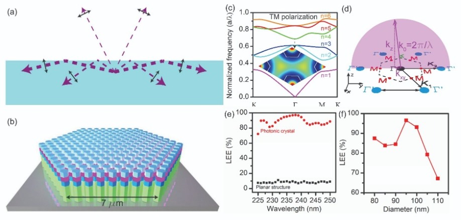
Figure 1. (a) Planar structures are impaired by a poor light extraction efficiency due to total internal reflection. (b) The light extraction efficiency is higher for a photonic crystal structure. (c) Photonic band structures are calculated for a lattice constant of 160 nm and a diameter of 95 nm. The electrical field intensity profile for the Γ point at the band n=4 indicates that there is a large overlap between the centre of nanocrystals and the maxima of the electric field intensity profile. This aids the output power of a nanocrystal LED. (d) Light with a wavelength of 240 nm has zero wavevector (Γ point at the band n=4). With a wavevector that is either zero or negligible in the horizontal plane, light emission is primarily coupled into the vertical direction. (e) Light extraction efficiencies calculated for a photonic crystal structure and a planar structure. (f) Variation in the light extraction efficiency with diameter. For more details, see X. Liu et al. IEEE Photon. J. 10 1 (2018).
At the University of Michigan we are trying to succeed on these fronts with arrays of AlGaN nanocrystals. This approach has much promise. One of its merits is that it is possible to realise a light extraction efficiency in excess of 90 percent by arranging nanocrystals in a photonic crystal structure, a geometry that is compatible with large-area LEDs. Taking this approach, we have produced devices spanning 210 nm to 360 nm that have efficient p-type doping, one of the issues in conventional devices. What’s more, we have made a low-threshold, electrically pumped nanocrystal laser operating at 369.5 nm, by engineering the optical properties via the photonic crystal structure.
Efficient light extraction
Mid and deep UV LEDs have an extremely low efficiency, due to the dominance of transverse-magnetic-polarized optical emission. In these devices, the electric field of the emitted light is parallel to the c-axis, due to the negative crystal-field splitting energy in aluminium-rich AlGaN. One consequence of this is that the majority of light is emitted out of the active region in the horizontal direction (see Figure 1 (a)), and it cannot be extracted out of the chip due to total internal reflection. The resulting light reabsorption inside the device is highly detrimental, leading not only to an extremely low efficiency, but also causing severe heating and device instability.
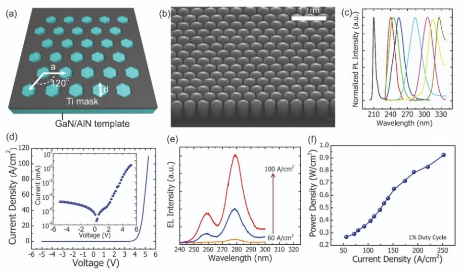
Figure 2. (a) Nanocrystal structures are produced by first patterning a growth mask on the substrate. (b) A scanning electron microscopy image of AlGaN nanocrystals formed by selective-area epitaxy. (c) Photoluminescence spectra of AlGaN nanocrystals with an aluminium-content varying from 20 percent to 100 percent. (d) Current-voltage characteristics of an LED based on AlGaN nanocrystals formed by selective-area epitaxy. Inset: Current-voltage characteristics plotted on a semi-log scale. (e) Electroluminescence spectra under varying injection current density. (f) Variation of output power with injection current density, measured using a pulsed biasing condition. For more details, see: X. Liu et al. Opt. Express 25 30494 (2017)
The benefits of the nanocrystals are so substantial that they can clear the bottleneck of light extraction, which has been hampering efforts to improve deep UV LEDs for many years. While extraction efficiency for planar structures is below 10 percent, in photonic crystals it can exceed 90 percent.
Note that the photonic crystal structures that we are investigating are not just designs for hero results in a lab. The architecture is robust, offering reasonable tolerance for deviations in dimensions. Even if the 95 nm target is missed and diameters vary from 80 nm to 100 nm, the efficiency of light extraction is still around 85 percent or more, implying that this device has much commercial promise.
Selective area epitaxy
The majority of III-nitride nanostructures are grown on foreign substrates through a self-organisation process. However, that is no good to us, as it creates nanocrystals with random diameters at random positions. Instead, we employ selective-area epitaxy to achieve site-controlled growth of nanocrystals with a well-defined size and position. This involves using a growth mask to promote the growth of nanocrystals on the template, in favour of growth in the apertures on the mask.
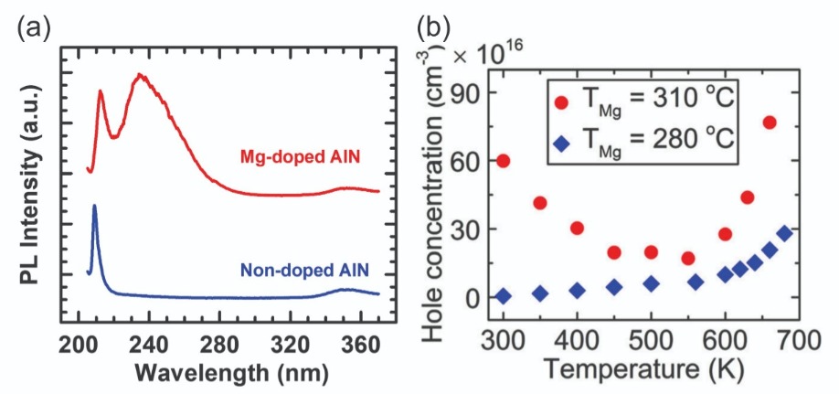
Figure 3. (a) Photoluminescence spectra for magnesium-doped AlN and non-doped AlN nanocrystals. (b) Variation of hole concentration with temperature for samples with two different magnesium doping levels (different magnesium cell temperatures). For more details, see; X. Liu et al. Photonics Res. 7 B12 (2019); and N. H. Tran et al. Appl. Phys. Lett. 110 032102 (2017)
We have fabricated LEDs from our nanocrystals. Plotting current as a function of voltage reveals excellent characteristics, with 50 µm × 50 µm devices showing a turn-on voltage of 4.4 V, and a current density of 100 A cm-2 at 5.5 V. This is a level of performance comparable to, or better than, that of a conventional AlGaN quantum-well LED.
Electroluminescence spectra reveal a peak at 280 nm, coming from emission from the active region (see the inset of Figure 2(e)). There is also a peak at 260 nm, due to electron overflow and resulting emission from the cladding layer. The output power produced by this device, measured at current density of 250 A cm-2, is 0.9 W cm-2.
p-type conduction
With conventional planar structures, one of the biggest barriers to realising high-efficiency with mid- and deep-UV LEDs and laser diodes has been the quality of the p-type current conduction. As aluminium content increases in the AlGaN alloy, p-type conduction gets more and more difficult, due to a larger activation energy and reduced hole concentration in the valence band. For example, for the typical p-type dopant, magnesium, the room-temperature activation energy in AlN can be as high as 500-600 meV. Consequently, only a tiny proportion of magnesium dopants are activated and contribute holes in the valence band. Compounding this issue, if the magnesium dopant is cranked up, this promotes the formation of donor-like defects, such as nitrogen vacancies. This self-compensation severely limits the magnesium concentration and ultimately restricts the hole concentration.
With nanocrystals, doping is a very different story. Thanks to efficient lateral strain relaxation, far less energy is required to substitute a magnesium dopant for an aluminium or gallium atom. This significantly enhances magnesium dopant incorporation. What’s more, the growth condition can be tuned to the nitrogen-rich regime, suppressing formation of donor-like nitrogen vacancies. The upshot is a far more effective incorporation of magnesium in the nanocrystal structure, compared with a planar structure.
Evidence for the enhanced incorporation of magnesium in nanocrystals is confirmed by a pronounced photoluminescence peak associated with a magnesium-acceptor-related transition at 235 nm (see Figure 3(a)). Measurements on AlN nanowire transistors reveal that the hole concentration at room-temperature reaches 6×1017 cm-3 in magnesium-doped AlN nanocrystals – that is seven orders higher than that in a magnesium-doped AlN epilayer. Our detailed investigations also suggest that the efficient p-type conduction comes from a combination of the significant reduction in activation energy for a portion of magnesium dopant, and hole hopping conduction in the magnesium impurity band. Both of these traits are enabled by the significantly enhanced magnesium-dopant incorporation in Al(Ga)N nanocrystals and suppressed defect formation.
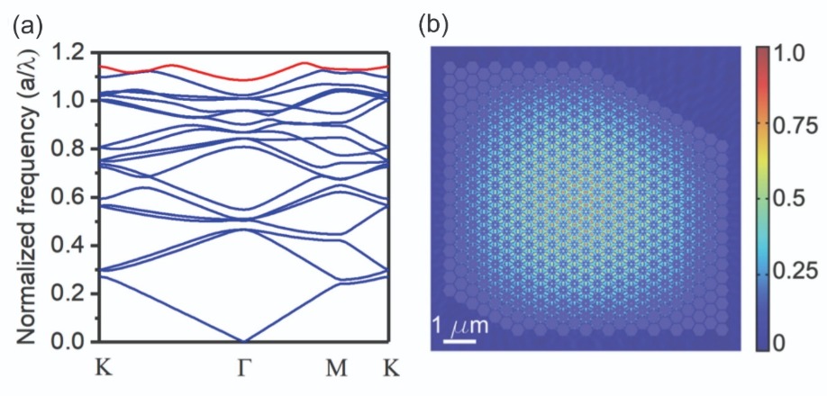
Figure 4. (a) Band structure of the designed photonic crystal structure targeted to operate at 370 nm with a lattice constant of 400 nm. The Γ point in the band in red colour is the designed operation wavelength. (b) The design of the irregular shaped nanowire photonic crystal, acting as a topological high-Q resonator, and the mode profile with a Q factor of 11,460. For more details, see: B. H. Le et al. Opt. Express 27 5843 (2019)
The performance of the UV laser diodes is held back by the lack of a high-reflectance mirror for optical feedback. Its absence results in a high threshold and severe heating.
One solution is to form a defect-free photonic nanocrystal structure that functions as a topological resonator with a high quality factor. Note that this architecture does not need extra mirrors for optical feedback. Designs with an arbitrary irregular shape can exhibit a high quality-factor resonance at the G point, a feature that is essential for the robustness of device operation.

Figure 5. (a) Current-voltage characteristics of the photonic nanocrystal laser. Inset: Current-voltage characteristics displayed on a semi-log scale. (b) Emission spectra of photonic nanocrystal lasers below (red) and above (blue) threshold current. (c) Variation of output with injection current. Inset: Variation of output with injection current displayed on a log scale. For more details, see: B. H. Le et al. Opt. Express 27 5843 (2019)
Our efforts show that AlGaN nanocrystals have many desirable properties, including negligible defects and dislocations, highly efficient p-type conduction, and efficient light extraction. All these strengths are difficult to realise with conventional AlGaN planar structures. Further work is now needed to develop efficient mid- and deep-UV optoelectronic devices, including LEDs and laser diodes, that are hampered by standard device architectures.
X. Liu et al. IEEE Photon. J. 10 1 (2018)
X. Liu et al. Opt. Express 25 30494 (2017)
X. Liu et al. Photonics Res. 7 B12 (2019)
N. H. Tran et al. Appl. Phys. Lett. 110 032102 (2017)
B. H. Le et al. Opt. Express 27 5843 (2019)
Arrays of back-emitting VCSELs are enabling a range of 3D sensing applications, from short-range facial recognition to long-range automotive LiDAR
BY JAMES FORESI AND LUKE SMITHWICK FROM TRILUMINA
3D sensing has crept quietly into common use. The advent of the iPhone X facial recognition system has enabled millions of people to interact with 3D sensing systems on a daily basis.
At the heart of these facial recognition systems is a class of laser known as the VCSEL – the vertical cavity, surface-emitting laser. The VCSEL enables structured-light depth-sensing analysis of an image. However, its attributes also make it an attractive option for other forms of 3D sensing, and it is being used in the automotive market to provide time-of-flight sensing, as well as LiDAR, for autonomous driving.
These applications are ensuring that the sensing market has a great future. According to figures from market analysts, global revenue for the 3D sensing market will climb from $2.1 billion in 2017 to $18.5 billion in 2023. That’s a compound aggregate growth rate of 44 percent that will help to spur sales of the VCSEL. By 2023, the market for just VCSEL illumination and associated optics will be worth more than $6 billion.
For the foreseeable future, VCSEL sales will rise across mobile, consumer, industrial and automotive sectors. In each of these sectors, there are different requirements for the illumination sources. However, despite these differences, there are five common considerations: wavelength selection, performance over temperature, reliability, range and cost.
VCSEL virtues
Sales of the VCSEL are rising far faster than its more common cousin, the edge-emitting laser, due to its superior attributes. Merits include its vertical architecture (see Figure 1 (a)), which simplifies production by removing the need for cleaving wafers and coating facets. After processing, all that is needed is to dice the wafer. Another feature of the VCSEL is its relatively short cavity, enabling high data rates. These strengths, plus the circular emission profile that is defined by the aperture, have made the VCSEL a very competitive and successful product for data communications, and are driving its success in 3D sensing. For the latter, higher output powers are required, realised by assembling arrays of apertures on a single die.
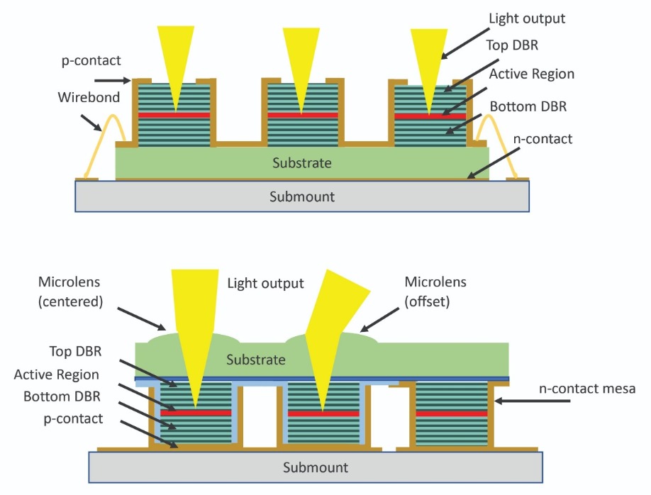
Figure 1. VCSEL designs feature a pair of distributed Bragg reflectors (DBRs). These reflectors provide the mirrors for a resonant cavity that contains the actives layers, featuring multiple quantum well structures. In a top-emitting VCSEL (a), light is emitted from the top of the wafer. This design requires wire bonds for electrical connection. In TriLumina’s novel, back-emitting VCSEL (b), light is emitted from the back side of the wafer. In this configuration, no wire bonds are required and lenses can be monolithically etched above the emitter to either reduce beam divergence (centred microlens) or shift the output angle of the beam (offset microlens). Note that the features are not to scale.
Our back-emitting VCSEL configuration has several notable advantages over its conventional sibling. It requires no wire bonds for electrical connections to the array – instead, the VCSEL die is simply flip-chip bonded to a sub-mount that has all of the required electrical connections defined. Thanks to the absence of wire bonds, back-emitting VCSEL die can be tiled close to one another to form large illumination modules that produce enough power for long-range sensing applications. In addition, eliminating wire bonds trims the parasitic impedance of the package, and in turn speeds rise and fall times, improving the performance for pulsed depth-sensing applications.
Another merit of back-side emission is that it allows micro-lenses to be monolithically etched directly into the emitting surface. Armed with this feature, beam shaping is possible: either reducing the divergence of each emitter, or diffusing light output. What’s more, lenses can be offset from the emitter aperture to steer the beam off-axis. This enables fully solid-state beam steering, by combining beam pointing with individual addressability of zones of the VCSEL apertures. Armed with these features, the overall system cost for 3D sensing can be reduced by eliminating optical elements or beam steering components.
What wavelength?
For engineers that design 3D sensing systems, one of their biggest decisions is the selection of the operating wavelength. Common lasing wavelengths include 850 nm, 905 nm, 940 nm and 1550 nm. The wavelength that an engineer selects will influence: eye safety; visibility, as sources that meet eye safety requirements can still be distracting; interference from ambient light; and the availability of sensors for detection. Note that all these considerations can impact other aspects of system design.
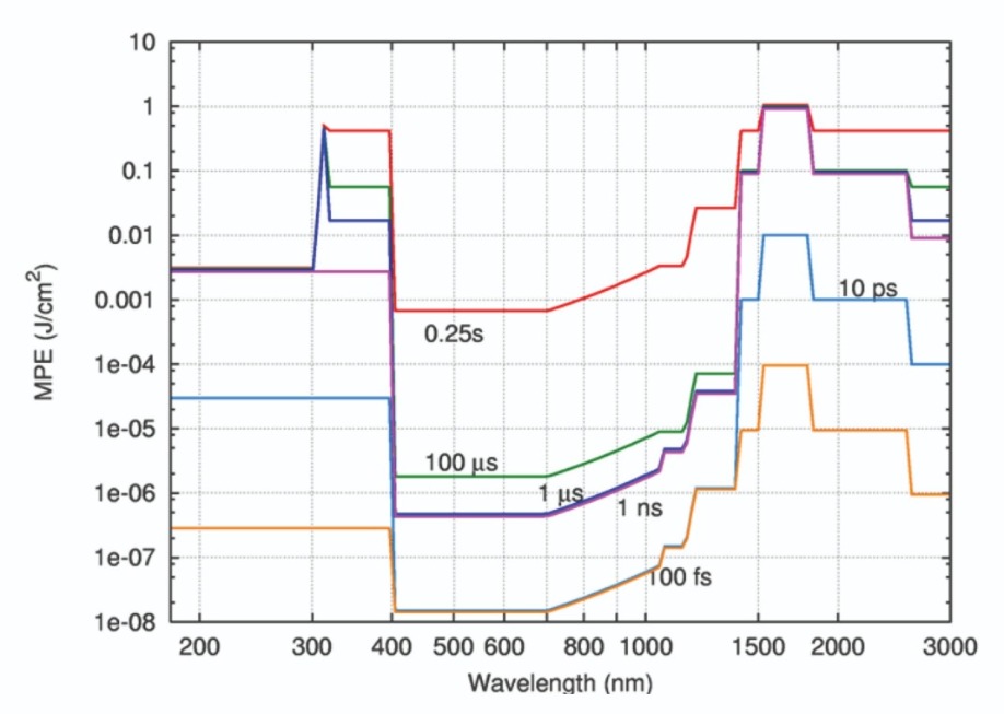
Figure 2. The maximum permissible exposure for eye safety, calculated as a function of wavelength and pulse width, for a fixed energy per pulse. For high-power point sources, eye safety configurations push systems to longer wavelengths. For VCSEL arrays, individual emitter output can be quite low, enabling eye-safe operation, even when the total array output is high.
VCSEL arrays typically operate at 850 nm to 980 nm. This might suggest, based on Figure 2, that eye safety would limit output powers compared to sources at longer wavelengths. However, it’s not that simple. That’s because eye safety considerations account for the difference between an array of lower-power sources and a single, high-brightness emitter, such as an edge-emitting laser. Far from the source, VCSEL arrays appear to be a single, circular output beam, and at these distances they behave like point sources. But as one gets closer to a VCSEL array, they become an extended source and eye safety considerations change, now being determined by the output of individual emitters. That’s welcome, as it can slash the overall power factors by up to four orders of magnitude, and make 940 nm VCSEL array sources nearly equivalent to point sources at 1550 nm in regard to eye safety.
Another consideration, which affects the performance and cost of the system, is the level of background illumination at or near the source wavelength. When background illumination is high, it must be suppressed with additional filtering. To gauge the level of filtering required, one can consider the solar radiation at air mass 1.5. Data provided by NREL (see Figure 3) reveals the level of background at the wavelengths 850 nm, 940 nm, and 1550 nm. At 850 nm, radiation is relatively high, and additional filtering is required for systems operating at this wavelength. Both 940 nm, which is not coincidentally where the iPhone X VCSELs operate, and 1550 nm, have reasonably low background radiation.
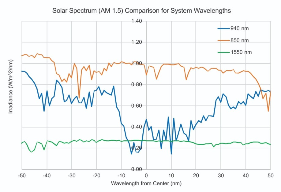
Figure 3. The AM 1.5 reference spectrum from NREL is shown centred at three different wavelengths (850 nm, 940 nm, and 1550 nm). Ambient solar light can become background noise in 3D sensing systems. To limit this background, systems can be formed at 940 nm or 1550 nm, rather than 850 nm.
Coping with the heat
All of the key markets for 3D sensing systems – consumer, industrial and automotive – require the optical source to maintain performance over an extended temperature range. The toughest requirements are found in the automotive sector, where operation may need to extend from -40 °C to +125 °C. This challenge is particularly tough because, to prevent system costs from escalating, the illumination source must ideally run without temperature control. Unfortunately, the characteristics of the laser change with temperature, including its wavelength and its output power.
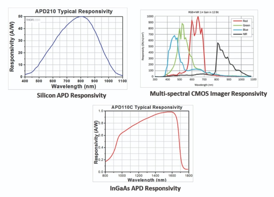
Figure 4. Responsivity, as a function of wavelength, for three different candidate sensors for 3D sensing systems. To trim system costs, silicon detectors and CMOS imagers are preferred over their more expensive III-V counterparts.
The shift in the output power of semiconductor lasers with temperature tends to be associated with the resonator mode and gain profile shifts, and changes in non-radiative recombination rates. The extent of the variation in power is strongly dependent on the design, but in a typical edge-emitter it can plummet to near zero at 85 °C. In contrast, our VCSEL arrays operate at up to 125 °C at close to 70 percent of the rated power at 25 °C (see Figure 5), meeting the most demanding automotive requirements without the need for temperature control systems.
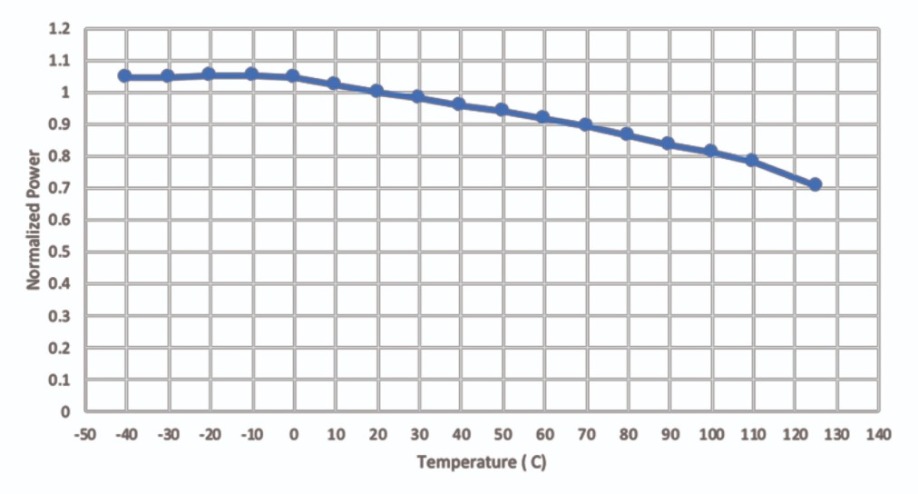
Figure 5. The output power of a TriLumina illumination module operating at 0.1 percent duty cycle (10 ns pulse, 100 kHz repetition rate), as a function of temperature. Output power is normalized to the output power at 25 °C. At 125°C, the illumination module still produces over 70 percent of its rated power.
Reliability is a key concern, especially in automotive applications where user safety is critical. Our VCSELs excel in tests to judge this characteristic, because the back-emitting architecture is inherently robust to the typical stresses used for assessing reliability. The n- and p- contacts sit on the same side of the VCSEL array, and are both entirely clad in metal or silicon nitride. Thanks to this design, there are no ingress paths for moisture into the active area of the device.
That’s not the case for the top-emitting VCSEL, which needs to have an opening in the p- contact to allow light to exit the device. It is only fair to point out that these top-emitting VCSELs have been shown to be highly-reliable – but we have no doubt that our back-emitting configuration provides even greater confidence for long-term operation. We find no evidence of degradation when driving our arrays under accelerated conditions for over 9,000 hours. We are now undertaking full evaluation of our 8 W illumination module to the automotive quality standard, AEC-Q102, and expect to complete qualification before this article is published.
Expanding the range
Depth-sensing systems use various approaches to determine distance. For short-range systems, either a structured light approach is adopted, such as in the iPhone X, or one based on stereoscopic vision. For medium to long-range systems, including LiDAR, the more common approaches are based time-of-flight. They can be either direct, using a flash; or indirect (see Figure 6).
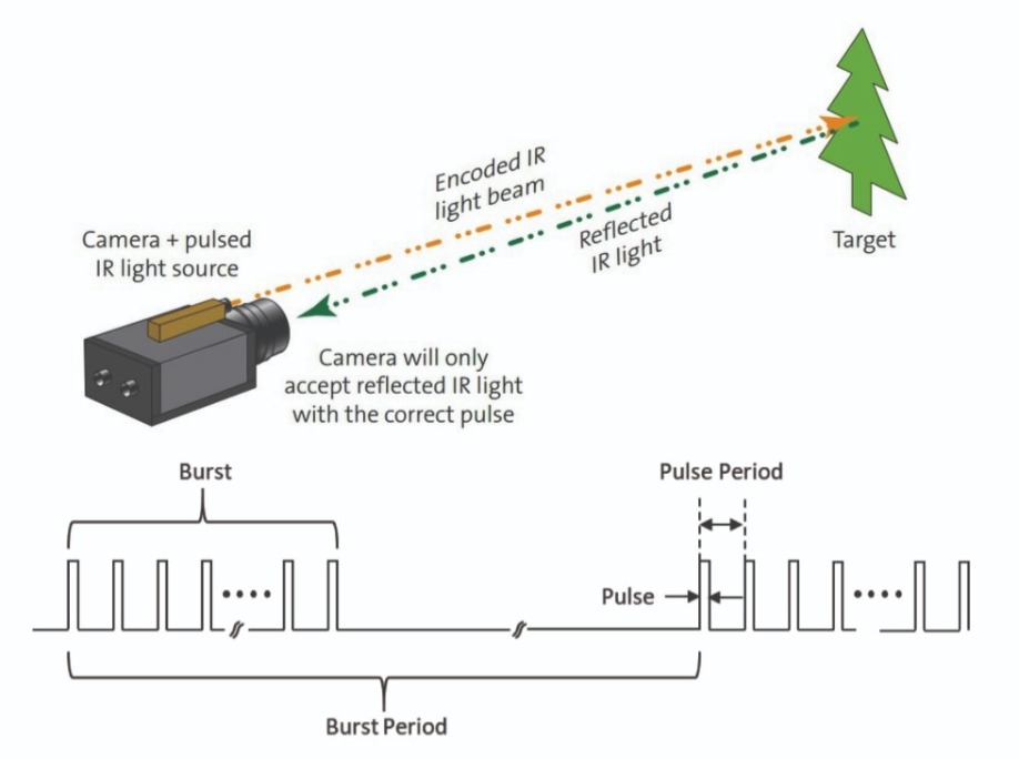
Figure 6. In a differential time-of-flight system, a pulsed infrared source illuminates an object with an encoded (pulsed) beam. The arrival time of the reflected pulse is measured with a detector or a camera system. The encoding scheme tends to employ a burst pattern, repeated at a burst period that corresponds to the maximum measurement range of the system. A notional burst pattern, shown here, can contain additional pulse patterns that allow the system to disambiguate multiple reflections, or other spurious returns.
Our lasers are going into short-range systems, providing a key ingredient in world-facing cameras for mobile applications. The unique advantage of illumination modules formed with our VCSELs is that they can be soldered directly to a printed circuit board, like any other electrical component. This makes them a low-cost option for replacing LEDs with VCSEL sources. Modules run at low duty cycles – typically a 1 percent to 3 percent average duty cycle – and they produce an output power of about 4 W.
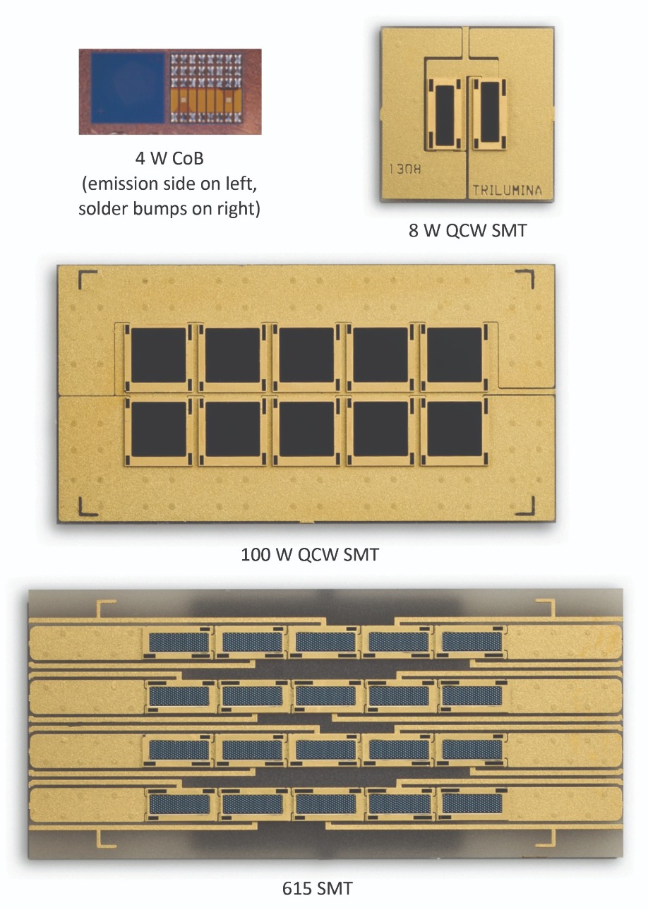
Figure 7. Examples of TriLumina’s illumination modules, for ranges from 5 m to 300 m.
For the 50 m to 100 m range, our illumination modules are being deployed in multi-mode time-of-flight cameras. These are used in indirect time-of-flight systems, featuring multi-spectral CMOS imagers that attain high-resolution depth maps, along with black-and-white and infrared images. The cameras are positioned at the four lamp locations on an automobile and enable the driver to benefit from increased awareness and safety. For this application, we produce 100 W modules, operating at a 2 percent duty cycle, formed from ten 2 mm x 2 mm VCSEL arrays on a ceramic sub-mount.
We ship 600 W illumination modules for the longest ranges. Assembled from twenty 1 mm x 2 mm die, and housed on a ceramic sub-mount, they are suitable for direct time-of-flight and flash front-facing LiDAR systems. To realise a narrow divergence – it is approximately 12 degrees, in terms of its full-width at half maximum – micro-lenses are etched into the chip. Using pulses as short as 10 ns or so, delivered at a 100 kHz repetition rate, LiDAR realises the specified range. Note that it is the low duty cycle of just 0.1 percent that allows the module to hit its high peak power.

Table 1. TriLumina illumination modules by range and application.
Looking ahead
VCSEL technology is continuing to make its way into new applications. The advent of the 3D sensing system has made the VCSEL array a very strong contender for infrared illumination. Armed with our back-emitting laser with integrated microlenses, we are able to offer a compelling product that helps to drive down the total system cost for advanced 3D sensing systems. The back-emitting configuration paves the way for higher levels of integration that will see VCSEL technology used in innovative designs at the forefront of 3D sensing.
By providing p-type doping, nitrogen-ion implantation promises to accelerate the development and commercialisation of vertical gallium oxide transistors
BY MASATAKA HIGASHIWAKI AND MAN HOI WONG FROM THE NATIONAL INSTITUTE OF INFORMATION AND COMMUNICATIONS TECHNOLOGY
To combat climate change, we need to generate far more clean electricity, and use this precious resource far better. Improvements must be made in motor drives, electrified transportation, data centres and the grid.
In all these applications, the performance of the power converters is governed by the characteristics of two core components: the diode, which controls the direction of current flow; and the transistor, which acts as a switch. Today, the majority of diodes and switches are made from silicon, but they are rapidly approaching fundamental performance limitations. Due to these constraints, commercial power systems are bulky and inefficient. What’s needed is the emergence of a portfolio of wide-bandgap semiconductors that will define a new generation of design for power conversion.
One material that has recently earned its citizenship within the compound semiconductor community is gallium oxide. Its hallmarks include an incredibly large bandgap that makes it a very promising candidate for high-voltage, high-power device applications, and the availability of large-size, high-quality wafers produced from melt-grown bulk single crystals. In addition to these two very attractive features, it is easy to dope Ga2O3 by ion implantation. This is a rare, yet technologically desirable property for any compound semiconductor.
For mass production of silicon and SiC devices, a key technology is ion-implantation doping. Its merits, compared with alternative process technologies such as re-growth and diffusion, include a higher degree of freedom and a considerable cost advantage for designing device structures.
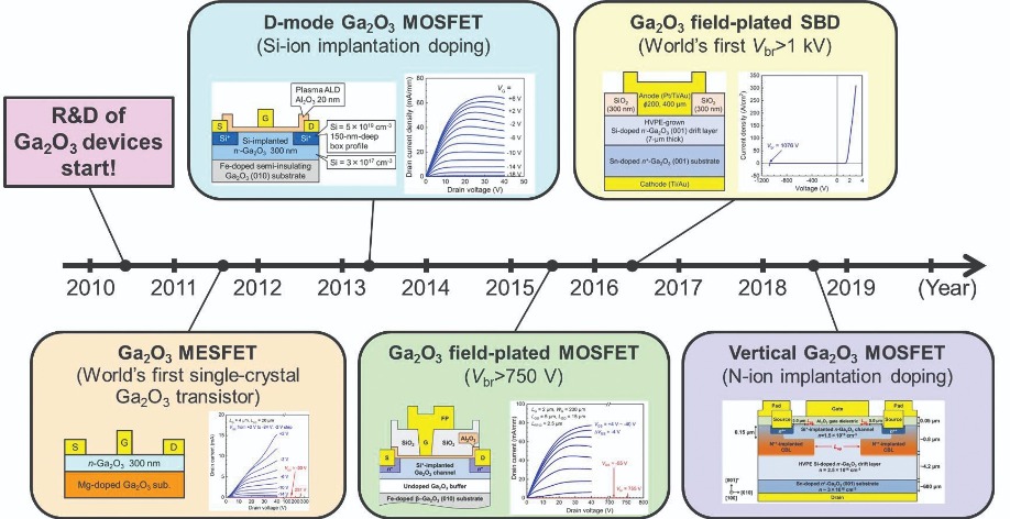
Figure 1. R&D history of Ga2O3 transistors and Schottky barrier diodes at NICT.
Weaknesses of the first Ga2O3 transistor, a metal-semiconductor field-effect transistor (MESFET), include large ohmic contact resistances for the source and drain electrodes. In addition, this device is held back by a lack of uniform, reproducible, n-type tin doping of the MESFET channel during crystal growth. This impediment stems from a narrow growth temperature window, making it very difficult to promote dopant incorporation into the material while maintaining high crystal quality.
To improve our MESFET, we have developed a silicon-ion implantation doping process. This allows us to trim the ohmic contact resistance by selectively forming heavily n-type Ga2O3 regions that shorten the metal–semiconductor tunnelling barrier thickness. Further benefits are that by using silicon-ion implantation for doping of the channel layer, we can employ higher growth temperatures that ensure optimal crystal quality – no longer do we have to worry about the possibility of irreproducible dopant profiles.
Thanks to development of our ion-implantation technology, we have been able to realise several milestones in Ga2O3 device technology. They include: depletion-mode MOSFETs; the world’s first Schottky barrier diodes with a breakdown voltage of over 1 kV; enhancement-mode MOSFETs; and very recently, vertical depletion-mode (D-mode) MOSFETs (see Figure 1).
Ion implantation doping
Most of our effort at developing n-type ion implantation doping of Ga2O3 has involved the addition of silicon. It forms a shallow donor, and with an activation energy below 50 meV, full dopant ionization is realised at room temperature. Typically, we activate the implanted silicon atoms with annealing at 800 - 1000°C. Even at these relatively low temperatures compared to those used to activate dopants in SiC, activation efficiency is really high: it is almost 100 percent for a silicon doping concentration of 1017 - 1018 cm-3, and between 60 percent and 80 percent for a concentration of more than 1019 cm-3.
While n-type doping is relatively easy, p-type doping is anything but. This has led the Ga2O3 community to endure a long struggle to uncover a suitable p-type dopant. Now, at last, the wait is over – recently, we have succeeded in developing an effective p-type ion implantation doping process using nitrogen as an acceptor.
Note, however, that it is not possible to obtain p-type Ga2O3 with effective hole conductivity. There are fundamental reasons why this is the case. One reason is that Ga2O3 lacks shallow acceptors with activation energies that are sufficiently small for ionisation at room temperature. According to several independent theoretical calculations, typical acceptor candidates for Ga2O3 – such as magnesium, zinc, beryllium and nitrogen – all have activation energies of 1 eV or more.
Additional reasons behind the lack of p-type Ga2O3 are related to its valence band structure, which is composed of oxygen 2p orbitals. Due to a very small dispersion in the band structure, holes have a very large effective mass – and calculations indicate that these positive charge carriers are impeded by a self-trapping effect associated with characteristic lattice distortions.
However, there is still a limited role that p-Ga2O3 can play – it is useful for engineering large energy barriers in the form of p-n junctions. We have done just that, with experiments confirming that a nitrogen-ion implanted Ga2O3 region formed in n-Ga2O3 can act as a current-blocking layer.
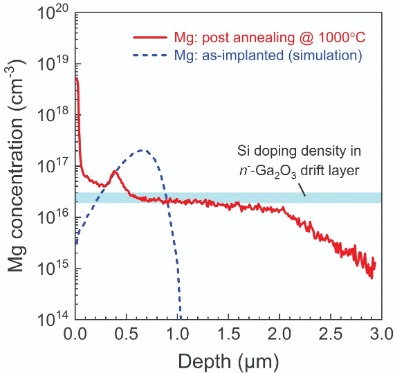
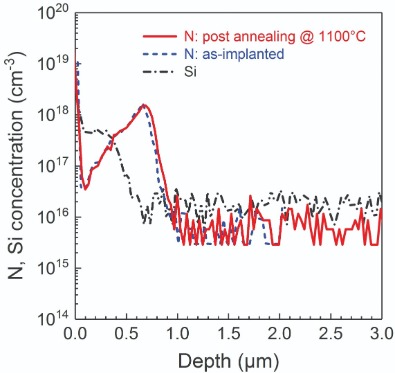
Figure 2 . Depth profiles of implanted (a) magnesium and (b) nitrogen atom concentrations before and after thermal activation annealing at 1000°C and 1100°C, respectively. All profiles were measured by secondary-ion mass spectrometry (SIMS), except for the simulated as-implanted magnesium profile. After annealing at 1000°C, the as-implanted Gaussian-like magnesium profile was transformed into a box-like one with a plateau concentration stabilised at the background donor concentration. On the other hand, absence of thermal diffusion was confirmed for implanted nitrogen atoms even after 1100°C annealing.
The background donor density determined the final distribution of the magnesium ions. Due to this, the as-implanted Gaussian-like magnesium profile transformed into a box-like profile, with a plateau concentration that was stabilised at the background donor concentration (see Figure 2(a)). We found that this happened for various concentrations of magnesium and the background donors, such as silicon and tin. Therefore, its occurrence was independent of both the impurity concentrations and the specific donor species.
Due to the rapid diffusion of magnesium, we switched to nitrogen, which is theoretically predicted to be an acceptor in Ga2O3, for p-type ion-implantation doping. The good news is that implanted nitrogen atoms are activated above 1100°C, and that thermal diffusion is insignificant compared with magnesium (see Figure 2(b)).
We have compared the current-blocking characteristics of magnesium- and nitrogen-doped Ga2O3 barrier layers fabricated in n-Ga2O3 by ion implantation and subsequent activation annealing (see Figure 3). Our measurements reveal that the current-blocking capability of the nitrogen-implanted barrier layer is vastly superior to that of the magnesium-implanted equivalent. For the nitrogen-implanted structure, the distribution of nitrogen atoms after the annealing process is nearly identical to the as-implanted profile; as a result, an n-p-n junction structure can be formed in the n-Ga2O3, and the nitrogen-doped p-Ga2O3 region can block electron current flow due to a large built-in potential at the n-p junction.
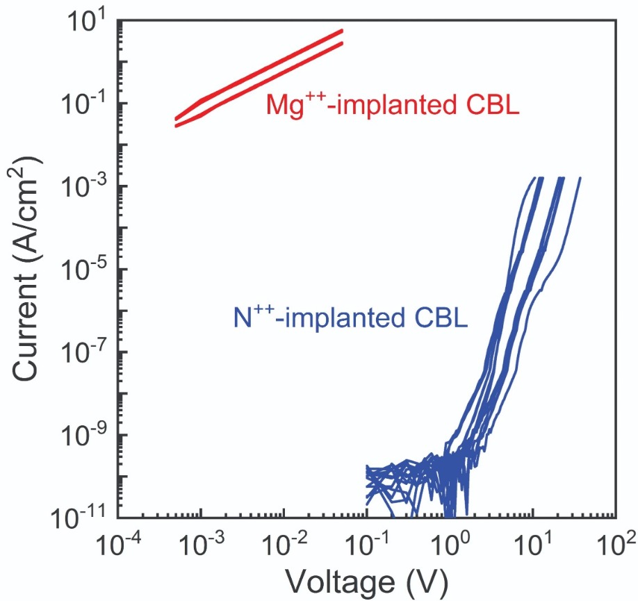
Figure 3. Comparison of vertical leakage current through nitrogen-implanted and magnesium-implanted current-blocking layers. The nitrogen-implanted region led to a much lower leakage current than the magnesium-implanted one.
Vertical transistors
We have employed our nitrogen-ion implantation doping process when fabricating normally-on D-mode vertical Ga2O3 MOSFETs. These transistors have a vertical architecture, because this is superior to a lateral one for realising high voltage ratings and high power levels. What’s more, it allows higher currents without requiring sizeable layout areas, and it enables far superior field termination, without much concern over surface-induced instabilities.
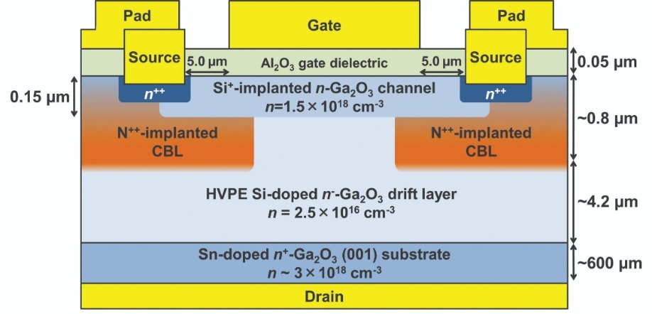
Figure 4. The vertical D-mode Ga2O3 MOSFET pioneered by NICT.
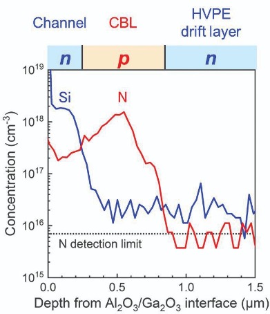
Figure 5. Depth profiles of implanted silicon and nitrogen atom concentrations in the overlapping region of the gate metal and the current-blocking layer of a vertical Ga2O3 MOSFET structure measured by secondary-ion mass spectrometry (SIMS). These data were obtained from a completed device. The depth profiles of both silicon and nitrogen atoms were just as designed.
While there is still much room left to improve the performance of our vertical MOSFETs, they are a breakthrough. The real value of this accomplishment lies in the use of multiple n- and p-type ion implantations to fabricate these vertical transistors, mirroring the process for making silicon and SiC devices. In other words, we have established a baseline process for future mass production of Ga2O3 power devices, and this greatly enhances the commercial prospects of this class of device.
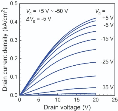
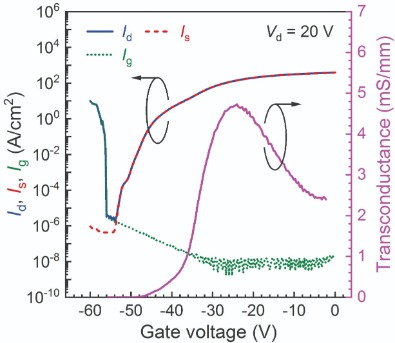
Figure 6. (a) DC output characteristics and (b) transfer characteristics of vertical Ga2O3 MOSFET.
Thanks to the high thermal stability of nitrogen in Ga2O3, there are unique opportunities for designing and engineering a variety of high-voltage Ga2O3 devices. It is worth noting that the p-type behaviour of nitrogen-doped Ga2O3 has also been observed for MBE-grown materials, in which nitrogen atoms are incorporated during epitaxial growth. However, many of the material properties of nitrogen-doped Ga2O3 are still unknown. It is also unclear how nitrogen atoms are incorporated in Ga2O3 lattice sites. Frankly, it is counter-intuitive to imagine that a nitrogen atom would displace and replace an oxygen atom in the Ga2O3 lattice, as an oxygen ion is very electronegative and its 2p orbitals are very stable. However, this picture is necessary to explain the activation of nitrogen atoms as acceptors.
Our work is helping Ga2O3 to rapidly emerge as the next major wide-bandgap semiconductor. In just the last few years, Ga2O3 transistors have taken enormous strides, such as the demonstration of kilovolt breakdown, normally-off operation, and the capability to form vertical devices. These breakthroughs are helping to position Ga2O3 as a strong contender for future technologies.
What’s needed now is to transfer the Ga2O3
transistors and diodes from the lab to the fab, so that commercial devices can start serving in practical applications. With the full support of the research community, which is establishing a more complete understanding of the materials and devices, this is a goal that can be reached by efforts directed at developing and building up the technologies. This will take time, but the payback will more than justify all the effort.
Masataka Higashiwaki and Man Hoi Wong thank Dr. Ken Goto, Prof. Hisashi Murakami, and Prof. Yoshinao Kumagai of Tokyo University of Agriculture and Technology for their collaborative contributions to HVPE growth in this work. This work was partially supported by Council for Science, Technology and Innovation (CSTI), Cross-ministerial Strategic Innovation Promotion Program (SIP), “Next-generation power electronics” (funding agency: New Energy and Industrial Technology Development Organization).
Further reading
M. Higashiwaki and G. H. Jessen. Appl. Phys. Lett. 112 060401 (2018)
A. Kuramata et al. Jpn. J. Appl. Phys. 55 1202A2 (2016)
M. Higashiwaki et al. Appl. Phys. Lett. 100 013504 (2012)
K. Sasaki et al. Appl. Phys. Express 6 086502 (2013)
M. H. Wong et al. Appl. Phys. Lett. 113 102103 (2018)
M. H. Wong et al. IEEE Electron Device Lett. 40 431 (2019)

InGaN lasers with wider wells produce an impresive performance, thanks to radiative transitions between excited states
Within the optoelectronic community, it is common knowledge that wells need to be thin to make high-performance GaN lasers. But this view is not correct, according to recent work by a Polish team from the Institute of High Pressure Physics and TopGaN – these researchers have shown that wide quantum wells can deliver an unexpectedly high optical gain.
The case against wide wells is based on a high piezoelectric polarisation, which creates a built-in field that pulls apart electron and hole wavefunctions, and ultimately diminishes the likelihood of radiative recombination. It’s argued that the thicker the well, the lesser the overlap of these wavefunctions.
However, according to team spokesman Grzegorz Muziol, what really happens is that beyond a certain thickness wells allow excited states with a high transition probability to emerge. “At the same time the transition probability between ground states drops more and more with quantum well thickness.”
Why has this encouraging behaviour taken so long to discover? Well, according to Muziol, the optoelectronics community did not expect to find such a substantial difference between the ground and exited states.
“In the case of conventional materials, such as arsenides and phosphides, there is no big difference between the ground and excited states,” points out Muziol.
Moving to wider wells produces relatively modest improvements in the threshold current density and the optical gain. “However, the sole fact that you can obtain optical gain in wide quantum wells is game changing,” says Muziol, who claims that this opens the door to new designs of laser.
The researchers demonstrated the virtues of wider wells by producing three different designs of ridge-waveguide, Fabry-Pérot laser. One features three 2.6 nm-thick wells, the second has a 10.4 nm-thick well, and the third a 25 nm-thick well.
All three design are formed on GaN substrates made by Ammono. These foundations have a threading dislocation density of typically 1 x 104 cm-2, and enable the fabrication of lasers with an extremely low degradation rate.
Lasers were made using standard processing steps. Fabrication involved SiO2 passivation, the evaporation of Ni/Au metal contacts on the p-side of the device, and the cleaving of mirrors.
Calculations with the SiLense 5.4 package highlight the merits of a thicker well. For a 2.6 nm-thick well, at no injection current the electron-hole overlap of the ground states is 0.19, rising to 0.39 at a current injection density of 100 A cm-2. For a 10.4 nm-thick well, at no current there is negligible overlap of both the ground states and first excited states. But crank up the current to 100 A cm-2 and the overlap between excited states is 0.56 – while for the ground states, it is just 0.0006.
Experimental results are broadly in line with these findings. For devices with either three 2.6 nm-thick quantum wells, or a single well that is 10.4 nm-thick or 25 nm-thick, the threshold currents are 3.2 kA cm-2, 2.8 kA cm-2, and 3.5 kA cm-2, respectively; and differential gains are 10.4 cm kA-1, 13.8 cm kA-1 and 11.7 cm kA-1, respectively.
When moving to wider quantum wells, there are concerns relating to the introduction of defects and compositional and thickness fluctuations. But none of these issues are present in the team’s devices.
Muziol and colleagues are planning to continue to explore the physics of excited-state transitions, and to design novel lasers that exploit the opportunities associated with wider wells.
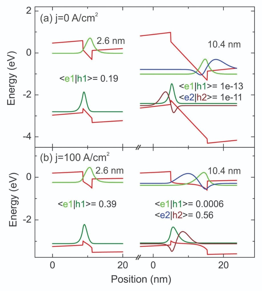
Band profiles, determined with the SiLense 5.4 package, reveal that at a current density of 100 A cm-2 the overlap of the first excited states in a 10.4 nm-thick quantum well is higher than that of the overlap of ground states in a 2.6 nm-thick well
G. Muziol et al. Appl. Phys. Express 12 072003 (2019)

Quantum cascade lasers operate with Peltier cooling
A partnership between researchers from ETH Zurich and Lund University is claiming to have raised the operating temperature for quantum cascade lasers (QCLs) emitting in the terahertz domain.
The team’s 3.9 THz lasers, which run at up to 210K, break new ground as they can be operated with a Peltier cooler. Up until now, terahertz QCLs have required cooling with cryogenic and helium-based technology.
This advance is a promising step towards compact, powerful terahertz systems employing Peltier cooling. They would combine terahertz QCLs with commercial detectors that are made from deuterated triglycine sulphate and already run on Peltier coolers.
Such systems could deliver non-invasive imaging and non-destructive quality assessments, and could be used for airport security screening and measuring the thickness of coatings.
The terahertz QCL made by the Zurich-Lund team is a two quantum well design. Prior to recent work, the maximum temperature for this form of QCL was 173K. Spokesman for the team, Lorenzo Bosco from ETH Zurich, attributes the improved performance of this latest two quantum well design to the combination of a more powerful and accurate simulation tool and superior processing technology.
To raise the operating temperature of the QCL, it is crucial to increase in the proportion of electrons in the upper state. One way to do this is to trim the number of states per period, a goal that is realised with a two quantum well design.
The team turned to non-equilibrium Green’s function modelling to optimise the design of their QCLs. Back in 2018, the team reported results on two-quantum-well QCLs, and their recent calculations suggest that improved performance can result from a shortening of the period and a thickening of the barriers.
To put this theory to the test, the Bosco and co-workers used MBE to produce QCLs with a thicker active region that reduced waveguide loss at the expense of a slightly higher mirror loss.
Devices were produced from a 3-inch wafer that had a thickness variation of 4 percent between its centre and its edge. This variation allowed the team to evaluate a portfolio of lasers, all with widths of 150 mm and lengths ranging from 1 mm to 2 mm.
The best laser, featuring relatively thin layers, is 1.8 mm long and able to lase at up to 210K. Driven with 50 ns wide pulses with a 415 Hz repetition rate, peak output at 10K is about 200 mW.
Increasing the temperature of the laser to just over 200K reduces the output of the QCL to around a milliwatt. “This power would probably be enough for some imaging applications and perhaps acousto-optics experiments,” says Bosco, but for most applications, he reckons that the source needs to have an output of hundreds of milliwatts.
One goal for the terahertz QCL community is to produce devices operating at room-temperature. “The higher the operating temperature, the smaller and more efficient the Peltier cooler can be,” argues Bosco. However, he points out that it’s not essential to eliminate the Peltier cooler. “Even mid-infrared QCLs, which reached room-temperature operation almost twenty years ago, still use a Peltier cell for temperature stabilisation.”
The work reported by Bosco and his co-workers did not included efforts to optimise the material composition within the QCL or its doping profile. The team are now looking into these opportunities.
“We have already achieved designs which are substantially better than the one shown in the paper, in theory,” says Bosco. “We will definitely keep working in this direction, and we are very hopeful that the performance of terahertz QCLs will improve in the near future.”
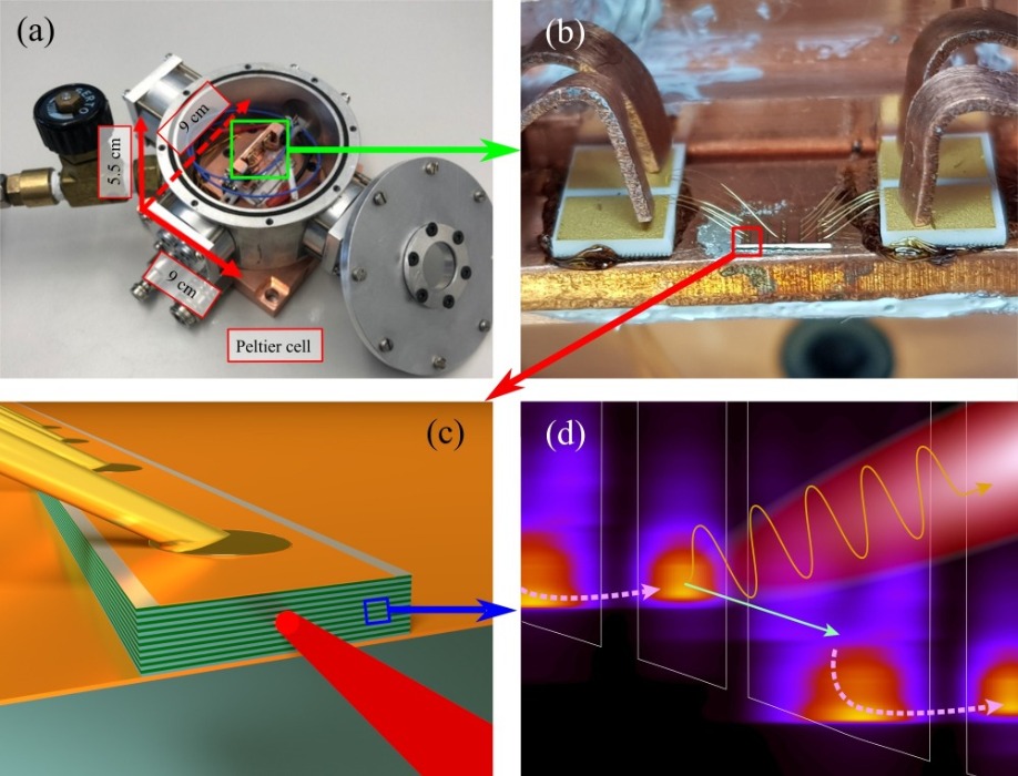
Peltier cooling (a) of the terahertz quantum cascade laser ((b) and (c)) that features a two quantum well design (d)
L. Bosco et al. Appl. Phys. Lett. 115 010601 (2019)

Switching to zirconium increases mobility in gallium oxide crystals
Gallium oxide is a very promising material for making electronic and optical devices, thanks to its ultra-wide bandgap, its transparency, its high breakdown field, and the availability of native substrates.
However, Ga2O3 substrates are not ideal. Conventional dopants, such as silicon, tin and germanium are unable to realise high doping, and they limit the conductivity of gallium oxide. But this problem is not insurmountable, with a team from the US reporting that progress can be made by switching to a zirconium dopant.
Recent work by this partnership – involving researchers at Washington State University, The University of Utah and Lawrence Livermore National University – has shown from both a theoretical and an experimental perspective that turning to zirconium allows the formation of n-type, highly conductive b-type Ga2O3 crystals with tuneable conductivity.
According to the paper’s lead author Muad Saleh from Washington State University, the mobility of zirconium-doped crystals is comparable to that of silicon and tin at a lower doping concentration – and mobility is higher with zirconium doping in medium- and high-doped crystals. Typical values are between 30 cm2 V-1 s-1 and 60 cm2 V-1 s-1.
These are encouraging results, given that this work is in its infancy. “As the growth process gets improved for any dopant, the mobility and electrical properties are known to improve,” argues Saleh. “So we believe the mobility with zirconium doping would improve further than its competition as we optimise our process.”
Zirconium-doped Ga2O3 crystals have been previously produced by the Verneuil method, also known as flame fusion. Powder is heated by an oxyhydrogen flame, with fusing and melting forming small droplets. However, crystals are limited in quality and size, restricting their use to scientific studies.
None of these issues occur when producing b-type Ga2O3 crystals from the melt, the approach adopted by the team. They began by preparing charges of Ga2O3 mixed with zirconium, and melting them in an iridium crucible with an RF induction coil. Crystals were grown with a zirconium content, defined in terms of atomic percent, of 0.1, 0.32 and 0.5.
Initially, crystals were pulled from the melt using the iridium seed, but this yielded polycrystalline material with a large grain size. So, the researchers slowly cooled the remains in the crucible with the vertical gradient freeze technique; and they also pulled a crystal still dipped in the melt, using Kypropoulos-style growth. Both techniques yielded large single crystals that were cleaved and cut with a wire saw.
Using these single crystals, the researchers determined values for mobility in zirconium-doped b-type Ga2O3 with Hall effect measurements. Decreasing the percentage of zirconium from 0.1 percent to 0.32 percent decreased mobility from 112 cm2 V-1 s-1 to 73 cm2 V-1 s-1, but a further fall in mobility did not result when the zirconium content increased to 0.5 percent.
The researchers have also measured the temperature-dependent electron density in their three samples. Fitting these curves provided values for the activation energy of 13 meV and 10 meV, for samples with a zirconium content of 0.1 percent and 0.32 percent, respectively. Calculations based on the Heyd-Scuseria-Ernzhof screened hybrid functional and projected-augmented wave approach are consistent with these results, suggesting that zirconium behaves as a shallow donor.
The team are continuing to study zirconium-doped b-type Ga2O3, with efforts directed at optimising the growth process and gaining greater insight into its conduction mechanisms.
“We have also found a different dopant that shows, both theoretically and experimentally, even higher mobility than zirconium doping with a higher free carrier concentration, which allows for higher conductivity materials,” says Saleh.
Crystals of β-type Ga2O3 cleaved along the (100) plane
M. Saleh et. al. Appl. Phys. Express 12 085502 (2019)
