
SEMICONDUCTOR MANUFACTURERS have witnessed a mixed bag of industry headlines following first quarter sales reports. Yet despite receding sales compared to 2018’s lofty highs, the SEMI trade group and independent analysts expect growth to return later this year or early in 2020.
In a SEMI forecast report published in late May, Walt Custer (Custer Group Consulting) stated that global electronic equipment shipments were up in April more than 2 percent compared to April 2018, but down compared to March tallies. Seasonality provided an early spring rebound, but Custer noted that year-over-year growth was minimal. Keep in mind that 2018 saw record performance after 2017’s breakneck growth. Factors pulling down 2019 sales forecasts include the continuing US-China trade dispute and memory chips struggling to recover after record-setting 2017 figures. Custer expects that chip and equipment sales will bottom-out later this year followed by a late year/2020 recovery. Stay tuned.
On a positive note for European manufacturers, attendees at the SEMI-sponsored Industry Strategy Symposium (April 2019) heard about ways that the EU is positioning and supporting its semiconductor industrial base for future growth. A key strength for Europe remains research and development hubs spawning new businesses in emerging sectors including photonic integration, sensors, IoT/IIoT and automotive autonomy along with established industrial leaders. Last December, the European Commission announced its IPCEI Microelectronics Project, which focuses on developing IoT and connected car technologies; 29 participating manufacturers and research organizations will receive Ä1.75 billion in public support while leaders are courting Ä6 billion in private investment.
In this edition of Silicon Semiconductor we take a look at key innovations that support a growing process tool and semiconductor equipment base. On the cover we feature Logotech’s new LP70 Multi-station Precision Lapping & Polishing System, which can process up to four 100mm or two 150mm wafers simultaneously.
Logitech has substantially automated wafer processing for silicon and III-V wafers, improving performance 40 percent compared to non-automated systems. We also hear from industry leader EV Group that is exploring new ways to accelerate the production of SAW-based devices through the use of new materials and packaging methods supported by the company’s advanced wafer bonding techniques. Sonoscan explores the benefits of combining high-frequency scanning with x-ray defect detection processes. And PVA TePla America delves into wafer cleansing techniques that support MEMS, flip chip and other advanced IC manufacturing requirements.

Rudolph Technologies has announced that a leading outsourced assembly and test facility (OSAT) has ordered Rudolph’s exclusive StepFAST Solution for panel-level packaging production, which includes a repeat order for the JetStep panel lithography system. Rudolph’s StepFAST Solution is a feed-forward adaptive shot technology that addresses process variations, die placement errors and dimensionally unstable materials that are common in existing and next-generation advanced packaging technologies. The elements included in the StepFAST Solution are Rudolph’s Firefly system for die position metrology, Discover software for advanced analytics, and the JetStep system for exposure.
“Uneven die placement on reconstituted panels, followed by die shift from the compression molding process, is a critical challenge for fan-out panel-level packaging,” said Alex Chow, vice president of strategic marketing. “Measuring the die placement prior to exposure is necessary to achieve overlay and yield thresholds, but measurement is not enough. Rudolph’s StepFAST Solution utilizes Discover software to analyze the error components and generate the appropriate correction file and exposure map for the JetStep lithography system to execute. Discover software automatically determines the optimal field size for exposure based on the overlay specifications and actual die placement error.”
“We are extremely grateful to have collaborated with this customer as they developed their ground-breaking panel packaging line using their first JetStep panel lithography system,” said Rich Rogoff, vice president and general manager of Rudolph’s Lithography Systems Group. “Their repeat order for a second JetStep panel system, which includes our StepFAST Solution, is a verification that our customers need complete solutions that provide a competitive advantage in the marketplace.”
The StepFAST Solution is exclusive to Rudolph Technologies and can double lithography throughput while providing 90% improvement on registration with feed-forward advanced process control. The Firefly system performs 2D defect inspection and die position metrology in a single pass, feeding critical metrology data to the Discover software engine to initiate the StepFAST Solution process. The method also provides a means to balance productivity (throughput) against yield, adding an extra dimension of flexibility for optimizing profitability. Systems and software are expected to ship in the fourth quarter.
TowerJazz and Vishay Siliconix has announced manufacturing portfolio expansion of existing and next-generation power semiconductor products for the automotive markets, to be produced in two of TowerJazz’s worldwide IATF16949 qualified manufacturing facilities. The newly developed automotive dedicated platforms will enable improved efficiency of power management circuitry in end products while reducing space requirements.
“With the ongoing increase of electronic content, automotive has been the main driver of growth in our industry. Ranking as Vishay Siliconix’s number one foundry while continuously supporting growing market activities, this expansion recognizes TowerJazz’s valuable continued commitment, exceptional technical and customer support, strong collaboration, and delivery performance,” said Serge Jaunay, Vishay MOSFET Division Head.
According to IC Insights, the automotive IC market reached record revenue of $32.3 billion in 2018 and is expected to remain the fastest growing IC market with a CAGR of 12.5%, exceeding $43 billion in 2021. This market is expected to be dominated by analog ICs, power management including power MOSFETs, visual and non-visual sensors, RF, and lighting.
Vishay Siliconix utilizes TowerJazz’s Transfer Optimization and development Process Services (TOPS) business unit for its world-leading low-and high-voltage power MOSFET products. These services provide best-in-class transfer methodologies, including the development of next-generation custom processes, technological capabilities with manufacturing capacity assurance and flexibility.
“We are excited to expand our long-term collaboration and business relationship with Vishay Siliconix, our highly valued customer and partner. The combination of both companies’ extensive technology expertise and market leadership, fosters an environment allowing mutual growth and success, enabling us to best serve Vishay Siliconix’s technological and operational needs”, said Zmira Shternfeld-Lavie, Senior Vice President and General Manager of Transfer, Optimization and development Process Services (TOPS) Business Unit.
Disco Corporation, a Japanese maker of semiconductor equipment, is investing around $156M (JPY 17.5 billion) to construct a new seismically isolated building at Nagano Works Chino Plant (Chino City, Nagano).
With the introduction 5G communication systems accelerating, the semiconductor and electrical components markets, including the development of IoT, self driving systems, and remote medical technology, are expected to expand. The demand for Disco’s precision processing equipment and tools is also expected to increase accordingly.
In response to the expected growth of these markets, Disco is expanding Kuwabata Plant (Kure City, Hiroshima). However, it was determined that further enhancement of the production system will be required.
In addition, most of the precision processing equipment and tools are currently produced in Kure and Kuwabata Plants, which are located in Hiroshima. Seismically isolated structures have been adopted in the buildings at both plants, and construction to ensure an independent water source has been conducted to protect against future water outages. However, the distance between the two plants is only about 10 km. Therefore, in order to prevent a situation where both plants cannot function should a disaster affect the entire area, resources must be divided further.
Samsung Electronics has announced that its 5-nanometer (nm) FinFET process technology is complete in its development and is now ready for customers’ samples. By adding another cutting-edge node to its extreme ultraviolet (EUV)-based process offerings, Samsung is proving once again its leadership in the advanced foundry market.
Compared to 7nm, Samsung’s 5nm FinFET process technology provides up to a 25 percent increase in logic area efficiency with 20 percent lower power consumption or 10 percent higher performance as a result of process improvement to enable us to have more innovative standard cell architecture.
In addition to power performance area (PPA) improvements from 7nm to 5nm, customers can fully leverage Samsung's highly sophisticated EUV technology. Like its predecessor, 5nm uses EUV lithography in metal layer patterning and reduces mask layers while providing better fidelity.
Another key benefit of 5nm is that we can reuse all the 7nm intellectual property (IP) to 5nm. Thereby 7nm customers' transitioning to 5nm will greatly benefit from reduced migration costs, pre-verified design ecosystem, and consequently shorten their 5nm product development.
As a result of the close collaboration between Samsung Foundry and its 'Samsung Advanced Foundry Ecosystem (SAFE™)' partners, a robust design infrastructure for Samsung's 5nm, including the process design kit (PDK), design methodologies (DM), electronic design automation (EDA) tools, and IP, has been provided since the fourth quarter of 2018. Besides, Samsung Foundry has already started offering 5nm Multi Project Wafer (MPW) service to customers.
“In successful completion of our 5nm development, we’ve proven our capabilities in EUV-based nodes,” said Charlie Bae, Executive Vice President of Foundry Business at Samsung Electronics. “In response to customers' surging demand for advanced process technologies to differentiate their next-generation products, we continue our commitment to accelerating the volume production of EUV-based technologies.”
In October 2018, Samsung announced the readiness and its initial production of 7nm process, its first process node with EUV lithography technology. The company has provided commercial samples of the industry’s first EUV-based new products and has started mass production of 7nm process early this year.
Also, Samsung is collaborating with customers on 6nm, a customized EUV-based process node, and has already received the product tape-out of its first 6nm chip.
Mr. Bae continued, "Considering the various benefits including PPA and IP, Samsung's EUV-based advanced nodes are expected to be in high demand for new and innovative applications such as 5G, artificial intelligence (AI), high performance computing (HPC), and automotive. Leveraging our robust technology competitiveness including our leadership in EUV lithography, Samsung will continue to deliver the most advanced technologies and solutions to customers.”
Samsung foundry’s EUV-based process technologies are currently being manufactured at the S3-line in Hwaseong, Korea. Additionally, Samsung will expand its EUV capacity to a new EUV line in Hwaseong, which is expected to be completed within the second half of 2019 and start production ramp-up from next year.
Synopsys has announced its collaboration with STMicroelectronics (ST) to establish a Center of Excellence program to speed development of automotive electronic systems and software. The program focuses on delivering Synopsys Virtualizer Development Kits (VDKs) for the ST Stellar family of automotive multicore microcontrollers (MCUs), enabling companies to accelerate the development of automotive electronic systems by enabling the move from physical to virtual testing. The first VDK with support for the ST Stellar MCU family is available today. Using a VDK enabled ST's automotive tier 1 customers to develop software and test patterns 18 months ahead of the first Stellar samples. Within a few days of receiving the first samples, the developed software was successfully executing on the sample hardware.
"New domain controllers that support data-enabled services require new tools to start software development early and accelerate system testing by moving from a physical to a virtual environment," said Fabio Marchiò, group vice president and general manager of ST's Automotive Digital Division. "Collaborating with Synopsys in their Center of Excellence program jumpstarted our customers' software development, accelerating their system development and testing."
Automotive tier 1 and OEM companies use VDKs to develop software early, before MCU or electronic control unit (ECU) hardware is available. VDKs enable the transition from physical to virtual system testing. Virtual environments increase testing throughput by frontloading test development, simplifying the execution of complex testing requirements, such as fault and coverage testing, and accelerating cycles by virtualizing testbenches and deploying them in regression, resulting in faster time-to-market, better quality, and more efficient testing turnaround.
ST's new Stellar family of automotive MCUs, based on multiple Arm Cortex R-52 and -M4 processors, and featuring extensive security that satisfies the automotive industry's demanding ISO 26262 ASIL-D safety qualification using lockstep capabilities, is designed for domain controller-based automotive platforms. The Stellar devices build on ST's extensive know-how and strong track record in high-performance automotive MCUs. Major applications for Stellar MCUs include smart control for hybrid powertrain, the broad electrification of car systems with on-board chargers, battery-management systems, and DC-DC controllers, as well as smart gateways, advanced driver assistance systems (ADAS), and enhanced vehicle stability controls. This collaboration brings together the unique expertise of both companies to help ensure the earliest availability of VDKs for the benefit of mutual customers.
"The increase in electronic content requires more productive tools and methodologies to start software development earlier, mitigate risks, and accelerate testing cycles," said Eshel Haritan, vice president of R&D for Synopsys' Verification Group. "By closely collaborating with STMicroelectronics for the development and delivery of VDKs, we can jointly ensure that automotive tier 1 and OEM companies have the most advanced, commercially-supported virtual prototypes and reliable long-term support for the ST Stellar family of microcontrollers."
Technoprobe, a provider of microelectronics/semiconductor test industry, has reached a definitive agreement to acquire Microfabrica Inc., supplier of in high-volume production, microscale Additive Manufacturing. This acquisition is part of Technoprobe's $100M USD 2019-2020 self-funded technological investment plan. Post-acquisition, Microfabrica will continue to operate independently out of its headquarters in Van Nuys, California.
"This acquisition marks a strategic step in our growth plans," said Technoprobe CEO Stefano Felici. "As technological leaders in our fields, joining forces will accelerate both organizations' development efforts, so we can launch a variety of breakthrough products aimed at the SOC and memory market segments. Our plan to further invest in Microfabrica will help the company expand its capabilities and achieve its global market potential."
Microfabrica CEO Eric C. Miller added, "We are very excited to join the Technoprobe family. The acquisition will not only provide a strong foundation for Microfabrica and our employees but will enable us to expand our process and materials capabilities and services, benefiting the entire industry. We look forward to engaging new customers as well as continuing to serve our current base as we have done in the past: satisfying all contracts, NDAs and production commitments."
ROHM recently announced the acquisition of a part of the diode and transistor business from Panasonic Semiconductor Solutions Company, a Group Company of Panasonic Corp.. The transfer is scheduled for October 2019 with ROHM handling sales of these products to Panasonic’s current customers thereafter.
Since the 1960s, ROHM has been developing, producing and selling semiconductor devices as a core business of the ROHM Group and has today the largest shares of the global markets for small signal transistors and diodes. Looking ahead, given the strong prospects of continuous growth in the automotive electronics, industrial equipment and other application markets, ROHM will be expanding its business in bipolar transistors, circuit protective Zener diodes, TVS diodes and other products. As a part of that, ROHM will proactively invest in a wide range of business resources in order to strengthen product lineups, further enhance product quality and ensure stable supplies. By acquiring the said business from Panasonic, ROHM aims to further expand its market share.
Details of the business acquisition
(1) Businesses handled by Panasonic Transistors (Bipolar, Built-in resistor, Junction field-effect)
Diodes (Schottky barrier, TVS, Zener, Switching, Fast recovery)
(2) To ensure a smooth transition and stable supplies to customers, ROHM will outsource production to Panasonic and maintain the exact same supply structure as before until the transfer is complete.
Going forward, both companies will be jointly preparing for the transfer of business, including obtaining all necessary approvals and permits. The transfer schedule details will be hammered out in the process.
EV Group (EVG) and Panasonic Smart Factory Solutions have announced that both companies have teamed up to provide a novel resist processing solution for plasma dicing that is developed for emerging applications, such as Internet of Things (IoT) sensors, MEMS, RFID, CMOS image sensors and thinned memories. This advanced solution, which incorporates the EVG 100 series of resist processing systems and Panasonic's APX300 Dicer Module plasma dicer, became available from March 13, 2019.
Plasma dicing enables highly parallel and high-throughput die singulation for small devices such as sensors, MEMS and RFID chips. It also provides debris- and particle-free die singulation to enable high process yields for CMOS image sensors, as well as damage-free and high-quality chip sidewalls for thinned memories.
Plasma dicing brings new pre-process requirements, including the need for thick resist coating (several dozen microns in thickness) on the wafer's surface prior to lithography or laser patterning processes to open up the dicing lanes. However, uniform protective coating of structures on the surface, such as multi-layer interconnections and bumps, is critical with traditional spin-coating techniques.
The EVG100 series of resist processing systems with EVG's proprietary OmniSpray technology enables conformal non-dependent to topography coating of surfaces and bumps across the wafer.
Panasonic has installed the EVG100 series in its Plasma Dicing Demonstration Center in Kadoma City, Osaka, Japan, to develop high-throughput and high-quality dicing solutions by leveraging its APX300 Dicer Module combined with the pre-processes of uniform resist coating on the bumps and subsequent patterning of dicing streets enabled by the EVG100 series.
EVG and Panasonic will begin providing this novel resist coating solution to improve dicing quality and productivity through customer demonstrations in the Plasma Dicing Demonstration Centre.
EPFL and MARVEL researchers have developed a new theory for heat conduction that can finally describe and predict the thermal conductivity of any insulating material.
Thermoelectric materials in particular hold vast potential for use in energy applications because they generate electricity from waste heat, such as that generated by industrial processes, by car and truck engines, or simply by the sun. Reducing the thermal conductivity of these materials by a factor of three, for example, would completely revolutionize existing waste-heat recovery, and also all refrigeration and air-cooling technology.
A unique theory for all insulating materials
In the paper Unified theory of thermal transport in crystals and glasses, out in Nature Physics, Michele Simoncelli, a PhD student at EPFL’s Theory and Simulation of Materials (THEOS) Laboratory – together with Nicola Marzari, a professor at EPFL’s School of Engineering and head of THEOS and of the MARVEL NCCR, and Francesco Mauri, a professor at the University of Rome–Sapienza – present a novel theory that finally decodes the fundamental, atomistic origin of heat conduction. Up to now, different formulations needed to be used depending on the systems studied (e.g., ordered materials, like a silicon chip, or disordered, like in a glass), and there wasn’t a unified picture covering all possible cases. This has now been made possible by deriving directly from the quantum mechanics of dissipative systems a transport equation that covers on equal footing diffusion, hopping, and tunneling of heat.
Waste heat recovery
This fundamental understanding will allow scientists and engineers to accurately predict the thermal conductivity of any insulating material (in metals, the heat is carried by the electrons, and that is well understood) – this is exceedingly important for thermoelectrics (i.e. materials that can convert heat into electricity), since these have both crystal- and glass-like properties, and are much needed for waste-heat recovery, or for refrigeration without greenhouse gases (and if you think refrigeration is boring, it is worth remembering that Albert Einstein spent many years trying to invent a new form of refrigerator).
In order to develop such next-generation technology, however, scientists first need to understand how and to what extent materials conduct heat. “Up to now, two different equations have been used for calculating thermal properties: one describes perfectly crystalline materials – that is, materials with highly ordered atomic structures – and the other one completely amorphous materials like glass, whose atoms do not follow an ordered pattern,” says Michele Simoncelli. These equations happened to work well in those special cases. “But between these two extremes lie a plethora of interesting cases, and neither equation worked – this is really where our contribution makes a profound difference”
Simoncelli, M., Marzari, N., & Mauri, F. (2019). Unified theory of thermal transport in crystals and glasses. Nature Physics. Advanced online publication. http://dx.doi.org/10.1038/s41567-019-0520-x
Picture credit: © Michele Simoncelli
Poor-quality organic semiconductors can become high-quality semiconductors when manufactured in the correct way.
The discovery that organic materials, such as polymers, can act as semiconductors led to a Nobel Prize in Chemistry in 2000. Since then, research within organic electronics has truly exploded, not least at Linköping University, which is home to world-leading research in the field.
Organic semiconductors, however, do not conduct current as efficiently as, for example, semiconductors of silicon or other inorganic materials. The scientists have discovered that one of the causes of this is the formation of traps in the organic materials in which the charge carriers get stuck. Several research groups around the world have been working hard to understand not only where the traps are located, but also how they can be eliminated.
Traps in organic semiconductors
“There are traps in all organic semiconductors, but they are probably a greater problem in n-type materials, since these are generally poorer semiconductors than p-type materials”, says Martijn Kemerink, professor of applied physics in the Division for Complex Materials and Devices at Linköping University.
Anvi Upreti, doctoral student at the Division for Complex Materials and Devices, who carried out the experiments together with the first author, Guangzheng Zuo. Picture credit: Charlotte Perhammar
Martijn Kemerink and his colleagues at Linköping University have concluded that water is the villain in the piece. Specifically, the water is thought to sit in nanometre-sized pores in the organic material and is absorbed from the environment.
“In a p-type material the dipoles in the water align with their negative ends towards the holes, which are positively charged, and the energy of the complete system is lowered. You could say that the dipoles embed the charge carriers such that they cannot go anywhere anymore”, says Martijn Kemerink.
For n-type materials, the water orients the other way around, but the effect is the same, the charge is trapped. Experiments have been carried out in which the material is heated, to dry it out and cause the water to disappear. It works fine for a while, but the material subsequently re-absorbs water from the surrounding air, and much of the benefit gained by drying disappears.
Manufacture in a dry atmosphere
“The more water, the more traps. We have also shown that the drier the films can be manufactured, the better conductors they are. The theoretical work by Mathieu Linares quantitatively confirmed our ideas about what was going on, which was very satisfactory. Our article in Nature Materials shows not only how to get the water out, but also how to make sure that the water stays out, in order to produce an organic material with stable conductivity.”
In order to prevent the reuptake of water into the material once it has been dried, the scientists have also developed a way to remove the voids into which water molecules otherwise would have penetrated. This method is based on a combination of heating the material in the presence of a suitable organic solvent.

Martijn Kemerink, professor of applied physics in the Division for Complex Materials and Devices at Linköping University. Picture credit: Charlotte Perhammar
General Rule for the Energy of Water-Induced Traps in Organic Semicondutors. Guangzheng Zuo, Mathieu Linares, Tanvi Upreti and Martijn Kemerink, Linköping University, Nature Materials 2019 DOI 10.1038/s41563-019-0347-y
Logitech describes key advantages of its new LP70 multi-station automated lapping and polishing system that can dramatically increase overall wafer productivity by 40 percent for almost all substrate materials.
The lapping and polishing of wafers used to manufacture semiconductors and optical devices is a time consuming task that can risk damage to expensive custom wafers worth in excess of (USD) $5,000 each if things do not go to plan. Logitech has substantially automated the process, speeding productivity and increasing repeatability by approximately 40 percent compared to non-automated techniques.
In wafer end fabrication, lapping and polishing processes have become more predictable, but there is often the need for a significant level of user expertise, guesswork and development time in order to optimise surface finish and repeatability. This can hamper the development of new technologies, especially as a process that is optimised at the pilot stage will often need to be revisited when transitioned to full production.
The path to better process control lies within Preston’s Law which provides a framework for predicting the amount of material that will be removed in a given time by lapping and polishing processes. By controlling variables using automated precision lapping and polishing systems with high levels of user control, operator variability can be minimised while process accuracy and greater repeatability can be achieved.
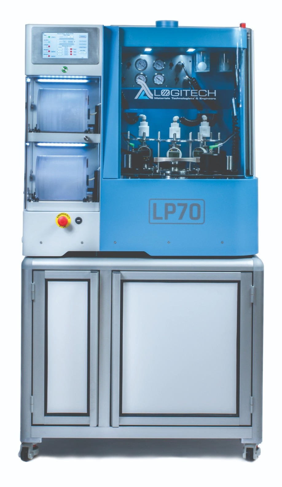
The Preston’s Law equation states that the material removal rate (MRR) is proportional to the product of the processing pressure/load/down-force and plate velocity. In the chemical mechanical polishing (CMP) process, polishing rates and overall accuracy are affected not only by the flow of the slurry and the characteristics of the polishing plate, but also by the mechanical action between the wafer and the plate, chemical reactions arising from slurry component molecules, and the interactions between these variables. Preston’s Law can be used to accurately predict the amount of material removed from a sample and confirm stability in the process. High degrees of process stability are possible by using a stable/accurate/repeatable processing platform such as the Logitech LP70 Multi-station Precision Lapping & Polishing System, which can process up to four 100mm or two 150mm wafers simultaneously.
Meeting demanding wafer requirements using manual lapping and polishing tools is hard to achieve with silicon, III-V or other very hard semiconductor wafer materials because of the high level of operator skill needed to manually stage and control such operations. Setup is a time consuming process that is not conducive to the high productivity that is demanded by semiconductor research and production facilities. Cost reduction in device production is driven by volume and yield. Automated systems designed to eliminate manual steps will ultimately increase productivity in wafer fabrication processes. The use of multiple work stations for simultaneous wafer processing will allow operators to achieve high throughput levels to keep up with the demand of their application.
Logitech’s Robin Armour, Process Development Engineer, frequently works with customers in the field who appreciate the precision of an automated systematic approach to wafer lapping and polishing. Robin has also been instrumental in the development of the LP70’s intelligent functionality to ensure it meets demanding customer requirements.
He notes that since the successful launch of the Logitech PM6 Precision Lapping & Polishing system, there has been increasing demand from both new and repeat customers based on the success of the PM6’s automated features.
“One requirement we see real demand for is increased levels of throughput on a single system whilst maintaining automated processes. The LP70 system has been developed from the same automated features as the PM6 with the increased throughput levels achievable to operators utilising four workstations on a single system rather than using multiple units – allowing for further cost reductions,” he remarked.
Silicon lapping & polishing
Every semiconductor wafer undergoes several common processing stages during manufacture including slicing the wafer from its crystal ingot, preparing the surface prior to fabrication and subsequent thinning of the wafer through lapping and polishing techniques.
After slicing, wafers made of silicon or III-Vs materials are lapped to remove surface scratches and flaws that occur during cutting processes. Typically performed by the wafer manufacturer, lapping removes saw marks and surface defects from the wafer and also helps relieve any internal mechanical stress that accumulated during the slicing process.
Lapping typically involves counter-rotating plates using an aluminium oxide abrasive with defined grain size distribution. During lapping, wafer flatness is improved while micro-roughness is also reduced. An edge grinding procedure may also take place. When edge grinding is needed manufacturers may also follow this step with polishing the wafer edge since doing this can greatly reduce the probability of wafer breakage further down the process line. Chemical mechanical polishing is the final material removal step utilized in manufacturing wafers. This process allows the attainment of super-flat, mirror-like surfaces with a remaining roughness on an atomic scale. Polishing the wafer can be seen as the most crucial step in the wafer manufacturing process since the polished wafer face is used as the base for device fabrication; it must be as damage free as possible. Typically, optimized CMP is achieved using a rotary or orbital motion of a chemical slurry injected in precise quantities and flow rates between the polishing plate and the wafer itself.
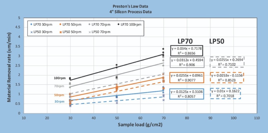
Chart 1: The chart illustrates performance advantages of Logitech’s LP70 compared to a predecessor system with fewer automated capabilities, the LP50. Utilising Preston’s Law in combination with other system enhancements, the LP70 can deliver approximately 40 percent total process time savings.
The LP70 has the ability to chart the removal rate data from the process jig and auto-plate flatness monitor in real-time utilsing the time weighted average (TWA) functionality. With this there is a need to accurately control the process by either stopping or programming an event action when the removal target has been reached, for instance, based on interaction of the process variables (plate type, speed, slurry flow rate, etc.) There is then the need to use data averaging to ‘smooth’ the process noise for increased accuracy on the target removal, using the central limit theorem. The amount of averaging is listed as a user control input field in the software, so the operator can optimise their process according to various needs. Removal rate data can be plotted real-time on the LP70’s graphical user interface (GUI); data can also be exported for further analysis via USB. This functionality allows operators to achieve increased levels of accuracy within their process that is easily repeatable.
Silicon lapping & polishing trials with the LP70
Lapping and polishing trials using a typical silicon substrate deployed in semiconductor applications such as manufacturing integrated circuits, solar cells and waveguide devices can be extremely revealing. In trials with the LP70, a series of steps was used, each with a different slurry solution, in sequence designed to replicate the steps a customer would typically undertake if they were lapping and polishing a production wafer.
Firstly, a coarse lapping process is utilized to remove material within 50 µm of the end point target. Previous experiments have shown that slurries containing AI2O3 particles measuring 20 µm provide the optimum balance between material removal speed and maintaining the integrity of the underlying silicon wafer. In a second stage, a medium/fine lapping process is conducted, during which a finer, less abrasive 9 µm AI2O3 slurry is used to remove materials to within 10 µm of the end point target. The final stage involves removing the last micrometres of material; the removal of any damage caused to the wafer during the lapping process is also undertaken using 32nm colloidal silica, such as the Logitech SF1 polishing slurry. After undergoing all three stages a typical surface roughness of Ra<1nm is achievable.
Tests with the LP70 to determine average silicon lapping at 50 rpm and 70 rpm showed an average 25 percent increase of material removal rates (MRR) in comparison to the LP70’s predecessor system, the LP50, that has fewer automated capabilities. LP70 features that allow for this increase in MRR are mainly: increased plate diameter; metered abrasive slurry distribution to each jig station and the driven roller arm. The LP70 also enables a 50 percent improvement on sample to sample (per workstation) end point thickness variation. Substantial time savings and greater accuracy were also achieved with the LP70’s automated set up and control platform. Collectively, all automation improvements delivered a total process time savings of approximately 40 percent, company research indicates.
Differentiating features found in automated systems such as the Logitech LP70 or PM6 Precision Lapping & Polishing Systems are key to achieving such impressive results. Intelligent controls on both systems have positive impacts on processing that not only benefit by creating a flatter, more defect-free wafer, but also in terms of substantial process time reductions. These technologies can help semiconductor optical device manufacturers to precisely optimise their sample preparation processes.
Conclusion
A high degree of geometric precision, flatness and parallelism can be achieved by taking advantage of automatic wafer thickness control. Software-driven set-up within automated systems permits faster processing times (in tandem with plate speeds of up to 100 rpm) and more reliable results. There is also extensive parameter control for the processing of complex and fragile wafers; metered abrasive feed supplies for optimal processing and reduced wastage of consumables are other substantial cost saving factors. Automated systems like the Logitech LP70 or PM6 also provide for the export of critical data that can be used as an information base for future process refinement and documenting productivity improvements over time.
Semiconductor and optical device manufacturers demand greater process control and real-time data in their quest for improved productivity and reliable, repeatable quality. By utilizing an automated approach in sample preparation such as the Logitech LP70 or PM6, researchers and manufacturers alike can achieve faster throughput, more precisely prepared and polished wafers, all with dependable repeatability that also frees their most highly skilled engineers and technicians to focus on other critical endeavours.
For further information on the capability of Logitech precision systems contact:
The continually growing demand for faster mobile data access and smart integration strategies is creating new and greater requirements affecting RF filter designers and manufacturers. EV Group examines ways to accelerate the production of SAW-based devices through the use of new materials and packaging methods supported by advanced wafer bonding techniques.
By Dr. Thomas Uhrmann, EV Group
Mobile technology has emerged as a primary engine of economic growth and transformed our everyday lives in a profound way. With each passing year, mobile technology’s spread throughout the world increases – through new types of electronic devices as well as new applications. Volume shipments of smartphones are expected to reach nearly 1.8 billion annually by 2021 [1]. Not surprisingly, global mobile traffic growth is also rising rapidly, with some estimates of traffic usage at 49 exabytes per month by 2021 [2]. These trends are leading to growing bandwidth demands and more crowded spectrum.
The migration from 3G to 4G and 4G LTE broadband wireless technologies has enabled multimegabit bandwidth, more efficient use of the radio network, latency reduction, and improved mobility – ultimately enabling faster download speeds. This in turn is driving a dramatic increase in the need for advanced filtering technologies, with some high-end, feature-rich phones today incorporating over 50 radio frequency (RF) filters [3]. The transition to 5G – driven not only by consumer demand for more graphic-processing-intensive applications such as augmented/virtual reality (AR/VR) but also the Internet of Things (IoT), the Tactile Internet, Industrial 2.0/IIoT, smart grid/energy and autonomous vehicles – will further drive new filter requirements [4]. These include different frequencies (and more of them), as well as steeper skirts in individual filter bands to reduce cross-talk between the bands and improve frequency accuracy.
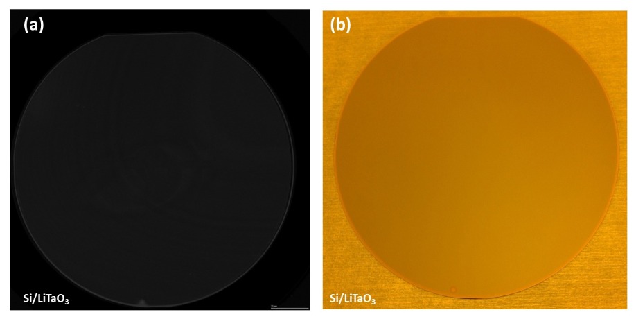
Figure 1.Lithium tantalate (LTA) bonded on silicon using LowTemp plasma activation (a) scanning acoustic image, and (b) photography of the bonded wafer pair.
Wafer bonding plays an important role in enabling the integration of new materials like LTA and LN on silicon in SAW filter manufacturing. This article will explore several wafer bonding technologies that are needed for both substrate processing and packaging of LTA- and LN-on-silicon based SAW filters.
Wafer bonding considerations for new substrate combinations
Bulk LTA and LN substrates possess unique optical, piezoelectric and pyroelectric properties that make them valuable for SAW applications such as RF filters. However, LTA and LN are very expensive as well as brittle materials, which make them prone to breakage and yield loss. In addition, LTA and LN are anisotropic materials, which have different linear expansion coefficients in different directions. RF filters built with these materials have a temperature yield drift, which makes it very challenging for the filter to stay on the designated band. As a consequence, the filter chip has to be physically broad – with relatively wide spacing of the interdigitated finger structures deposited on the filter – in order to compensate for the temperature-related shift and remain on the designated band while maintaining good filtering properties with little to no signal degradation.

Figure 2. Example of a plasma-activated wafer bonding process flow.
Wafer bonding challenges
Direct wafer bonding is a bonding approach that enables the combining of two different materials with different lattices and coefficients of thermal expansion (CTEs) without any additional intermediate layers. The bonding process, which is based on chemical bonds between two surfaces that are established by elevating the temperature of the surfaces and applying pressure, can be used to enable LTA/LN on silicon. However, there are several key considerations with direct wafer bonding:
Current methods of manufacturing LTA and LN wafers are generally less sophisticated compared to silicon wafer manufacturing. For example, bright polishing is often used instead of chemical mechanical polishing (CMP), which is insufficient for properly conditioning the wafer’s surface prior to bonding. In addition, the CTE of the two materials differs significantly from silicon (by a factor of 3 in the case of LN, and by a factor of 4-6 depending upon direction in the case of LTA) [5]. As a result, even bonding at temperatures lower than 200°C results in cracks, which cause massive yield loss. However, treating the surface of the silicon substrate with plasma prior to bonding the LN/LTA layer allows the annealing temperature to be reduced to 100°C, which in turn eliminates voids and cracking (Figure 1). In addition, a pre-cleaning step prior to plasma activation can eliminate surface roughness and particles to ensure maximum bonding yield [6]. Plasma-activated wafer bonding thus provides an ideal process for manufacturing temperature-compensated SAW filters. Figure 2 illustrates a typical plasma-activated wafer bonding process flow.
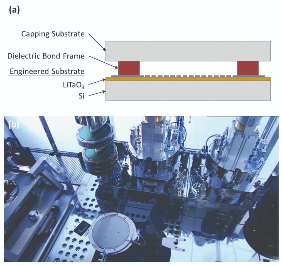
Figure 3a: Example of a SAW filter;
Figure 3b: Internal view of an adhesive wafer bonding chamber.
Packaging has a very high impact on the size of RF filters. To support filter scaling, future packaging needs for RF filters (including those based on LTA and LN-on-silicon) are being driven by the industry trend toward “modularization”, where individual RF filter components are being bundled into filter bank modules rather than integrated individually. Whereas with the earliest cell phones, individual band filters would be used for different area codes and packaged separately, more recent models are incorporating modules that may encompass all area codes in a country or region. The resulting module is a discrete device, yet ends up being extremely bulky to cover all the functionality within.
Modularization is occurring as a result of a combination of factors, including industry consolidation and customer segmentation, which is driving wireless chipmakers to acquire component manufacturers as a means of gaining competitive advantage and greater market share. Recent examples include the formation of the Qualcomm-TDK joint-venture RF360, Avago’s acquisition of Broadcom, and the merger of RFMD and TriQuint resulting in the formation of Qorvo. This has led to the creation of the front-end module market with a few key players and preferred customers (handset device makers). For smart phone manufacturers, a major benefit of modularization is the fact that they can manage a single supplier. For the RF/wireless device manufacturer, the greatest benefit for the design winner is gaining a larger piece of the business. However, the reverse is true for the companies that lose out on the design win, as they are at risk of losing a greater share of the overall RF market.
Modularization is not simply packing more filters into a device, however. The filters themselves are also becoming more complex. For example, several different frequency bands are being manufactured on the same area on the same chip. Advanced wearables such as smartwatches with wireless connectivity have stringent footprint requirements and cannot afford to incorporate bulky filter modules. Smart phones also have stringent requirements when it comes to product thickness as well as improving energy efficiency.
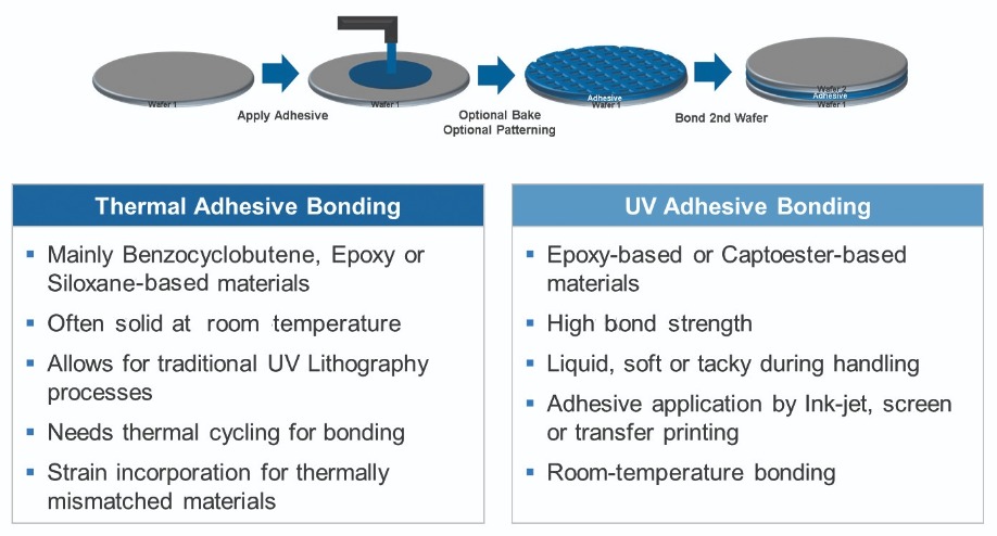
Figure 4. Adhesive wafer bonding process flow and comparison for thermal and UV bonding
Wafer bonding for RF WLCSP
In the case of SAW filters, a polymer frame surrounding the outside of the device is needed in order to create a cavity between the interdigital transducers (IDTs) that are fabricated on the surface of the LTA/LN substrate and the cap wafer. This allows for free movement of the acoustic waves across the top surface of the device wafer. The IDTs are simple lithographic finger structures that do not oxidize, and thus hermetic sealing is not needed. From this perspective, the design requirements of SAW filters are quite relaxed compared to Bulk Acoustic Wave (BAW) filters and many MEMS devices. As such, adhesive/polymer wafer bonding is an ideal bonding approach for SAW filters both from a technical and cost perspective. Figure 3a shows a typical SAW filter, while Figure 3b provides an overhead view of the inside of an adhesive wafer bonding chamber.
Adhesive bonding is a very simple process compared to other bonding approaches with fewer required wafer preparation steps, as shown in Figure 4. It is a low-temperature process (typically 200-300˚C), which requires less time to ramp up the temperature within the bond chamber. This results in higher bond chamber utilization and a faster bonding process. At the same time, the lower-temperature bond process allows for a wider variety of bonding materials to be used. Adhesive bonding also has a high tolerance for the underlying topography of the wafer, as well as relaxed requirements for overall surface quality and particle contamination.
When using a bulk LTA or LN substrate for SAW manufacturing, the cap wafer is composed of the same material to ensure CTE matching. With LTA- or LN-on-silicon substrates, however, the composition of the cap wafer is no longer limited to these more expensive substrates. Manufacturers have the freedom to use silicon or even glass substrates for the cap layer, which can significantly drive down the cost of manufacturing. Glass can also be bonded as a cap wafer at room temperature using ultraviolet (UV) wavelength.
Areas for future development
As we have discussed in this article, substrate property engineering is vitally important for temperature compensated SAW filters. In addition to low-temperature, thermally-activated adhesive bonding, adhesive research is also focusing more on photonic crosslinked adhesives due to the growing demand for photonic wafer bonding to enable the production of liquid crystal on silicon (LCOS) displays, photonic sensors and wafer-level optics (WLO). UV-based wafer bonding enables room-temperature bonding without any strain incorporation, as well as enables high-throughput processing and the possibility of encapsulating different materials and gases with accurate environmental control.
Summary
The growth in mobile data traffic as well as the growing trend of smart integration in mobile devices is driving greater demands in RF filter technology. SAW filters are both increasing in quantity as well as complexity in smart devices, resulting in modularization and consolidation, which is fundamentally changing the RF mobile communication market. New materials and packaging methods supported by wafer bonding in SAW filter manufacturing are needed to support these trends. Plasma-activated wafer bonding is an enabling technology for manufacturing SAW filters on new material combinations offering higher performance and lower cost such as lithium tantalate- and lithium niobite-on-silicon. When considering new packaging approaches such as WLCSP that offer greater density, improved performance, scalability and lower cost, adhesive bonding is the wafer bonding method of choice.
[1] IDC Worldwide Quarterly Mobile Phone Tracker, March 1, 2017
[2] Cisco® Visual Networking Index (VNI) Global Mobile Data Traffic Forecast Update, 2016-2021 White Paper, March 28, 2017
[3] ibid
[4] J. Kimery, “Is 5 G for Real?”, EDN, November 2, 2017
[5] CCW Ruppel, “Acoustic Wave Filter Technology-A Review”, IEEE Trans Ultrason Ferroelectr Freq Control. 2017 Sep;64(9):1390-1400
[6] N. Razek and V. Dragoi, “New developments in plasma activated bonding for various materials combinations”, Proc. Wafer Bond Conference 2015
A pulse of ultrasound traveling through a solid is attenuated as it goes and is reflected and/or transmitted by material interfaces. An x-ray beam is also attenuated but ignores material interfaces. An ultrasonic pulse must be inserted at 90° to the surface, but x-ray can be inserted at almost any angle. The usefulness of these and other differences is described.
By Tom Adams, consultant, Nordson SONOSCAN
A pulse of ultrasound is speeding through a layer of copper at a speed around 4700 meters per second. As it moves, the pulse is mildly attenuated - meaning that it is gradually losing energy (amplitude). Suddenly it runs smack into a layer of cured epoxy. One portion of the pulse sails right across the interface between the two solids and keeps going into the epoxy. The other portion is reflected back, at the same speed with which it arrived, to the transducer that launched the pulse.
An x-ray beam travels through the same copper layer. Like the pulse of ultrasound, it is somewhat attenuated by the copper through which it is moving. When it runs into the wall of cured epoxy, the x-ray beam keeps right on moving; none of it is reflected. What does change is the rate of attenuation, because the beam is now traveling through a different material.
When both an x-ray system and an acoustic micro imaging tool are used on the same sample, examining both images can give information that can shed light on quality control or failure analysis questions. Neither energy form causes any physical damage to the part, and it is hard to think of a physical anomaly that can hide from both.
Because it is part of the electromagnetic spectrum, an x-ray beam’s velocity through a material is so high it requires no attention. When imaging a sample, the size of the beam fired from the x-ray tube expands as it moves. The x-y area of the image (magnification) is adjusted by changing the distance to the target.
The speed of ultrasound through a solid is many orders of magnitude less than the speed of an x-ray beam. A 100 MHz pulse, for example, moves through mold compound at about 3,000 meters per second. And ultrasound is launched not as a continuous beam, but as a pulse whose return echo represents an interface area measured in microns. The echo will become one pixel in the visible acoustic image. The transducer launches thousands of pulses per second as it scans, and, where there is an interface in the line of fire, collects thousands of echoes per second.
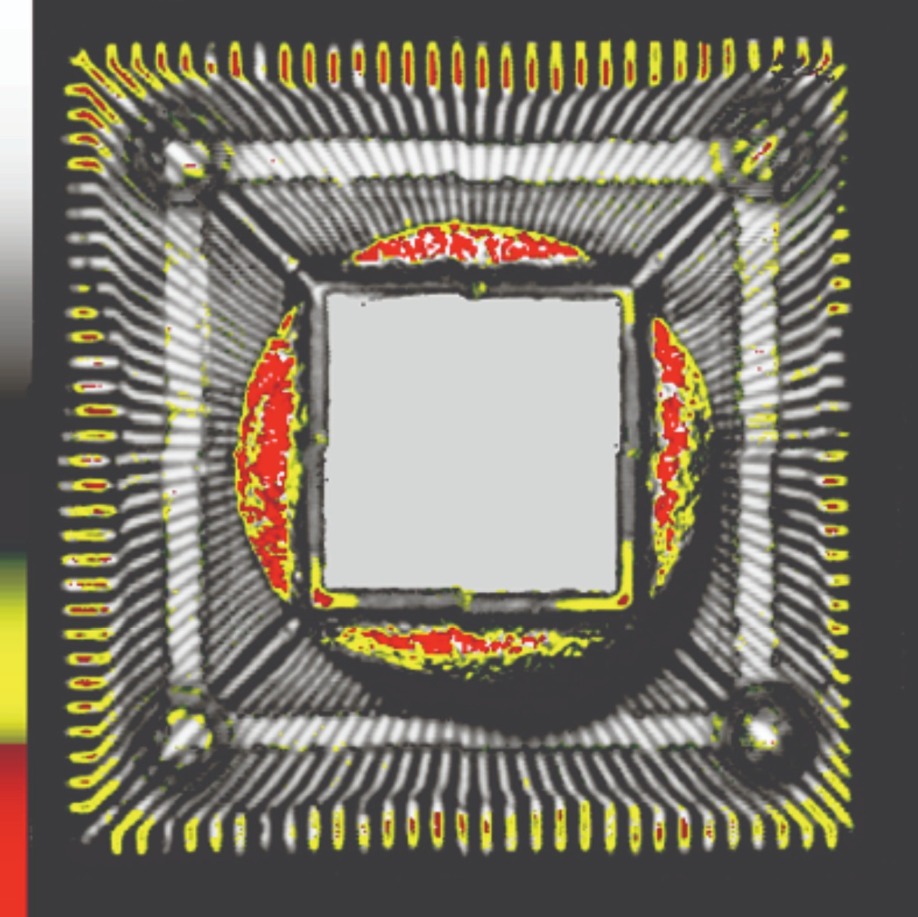
Figure 1: Air gaps in this PEM are red and yellow because they reflect nearly all of the ultrasound. Black regions reflect none.
Where no echoes were received (between the lead fingers, for example) the pixels are black. The color map along the left side of the image indicates that the echoes reflecting nearly all of the launched pulse are red. The circular red-yellow feature surrounding the die is a crack through the mold compound surrounding the die. The distal ends of most of the lead fingers are also red and yellow.
To the southeast of the circular crack is a curved black area that looks like an optical shadow - but this is an acoustic image. What happened is this: as the crack traveled upward, its path became more vertical. Where it is somewhat level, the crack reflects nearly all of the arriving pulse, and the crack is red. Where the crack becomes more vertical, the crack is yellow (the next color up on the color map at left). Where the path became even steeper, all of the pulse was deflected (echoed) at an angle and no echo was sent upward to the transducer, so the pixels in this area are black (no signal received).

Figure 2: Because x-ray is hardly attenuated by air and not reflected by interfaces, the crack does not appear in this image of the same part.
The wires in the PEM shown in Figure 1 were then imaged separately by the Quadra 7 in a region where the wires are bonded to pads on the lead frame (Figure 3). What has happened is clear: the stresses set up by the expanding popcorn crack stretched the wires until they broke and became disconnected from the pads they had been bonded to. The resolution is high enough that details of the break can be seen, along with the wire’s former connection location on the pad.

Figure 3: An x-ray closeup of part of the device shows broken wires.
Figure 4 is the x-ray image of a different device having a die that is eutectically bonded to a ceramic substrate. The lid has been removed to expose the bare die. There is no mold compound. The depth of interest was the die attach, where there may be voids in the eutectic that are efficient blockers of heat radiating from the die.
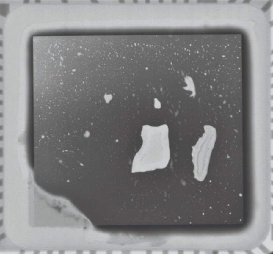
Figure 4: X-ray image of a device having a ceramic substrate and eutectic die attach.
At the lower left corner is a very large area where there is no eutectic material, although there are traces of die attach material along the upper right margin of the area. In general, voids in eutectic bonds can form in one of two ways: either the eutectic material melts and flows away, or the pressure applied is not sufficient to make a bond. If the eutectic material is present but did not form a bond, then x-ray will not detect this condition. This large void was probably formed by the melting and subsequent migration of the eutectic material.
The same device is imaged acoustically in Figure 5. Far more voids - and especially tiny voids - are visible here than in the x-ray image. Many voids appear white because they are large enough - even if their overall shape is somewhat spherical - to reflect enough of the pulse to create a visible group of white pixels. Voids smaller than these simply scatter nearly all of the arriving pulse and are black in this acoustic image. Both of the largest voids, which in the x-ray image displayed some internal structure, show no structure here because essentially all of the pulse is reflected by the solid-to-air interface and none enters the void itself.
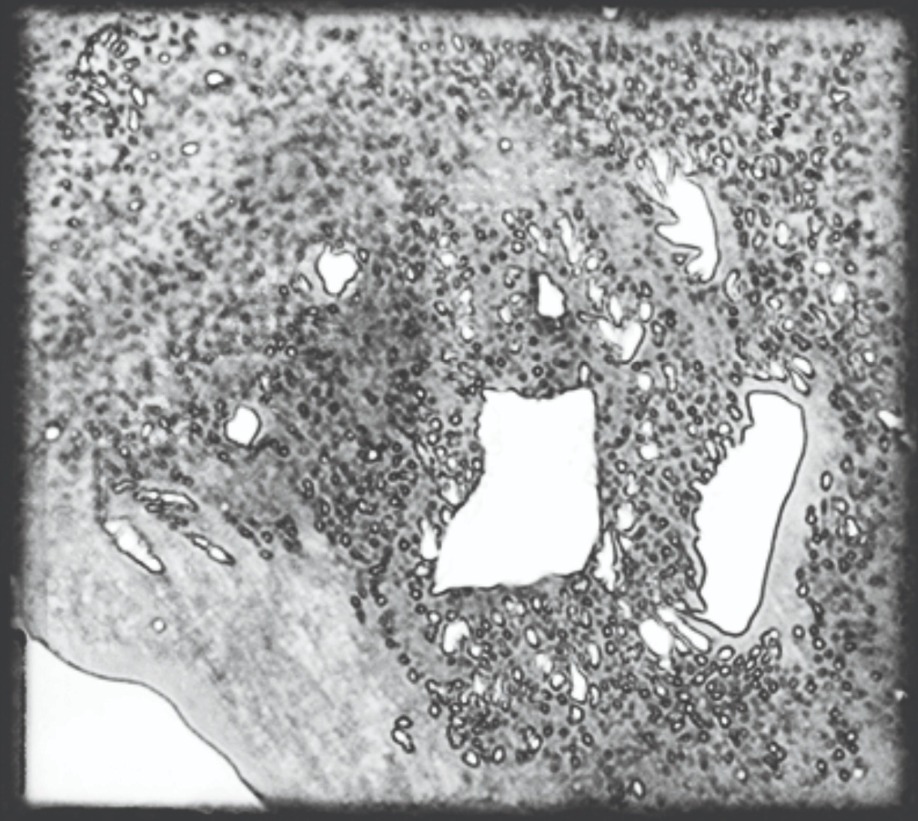
Figure 5: Acoustic image of the same device
A small area near the center of Figure 5 is shown magnified in Figure 6, where it can be seen that even some of the smallest voids have brightly reflecting centers.
Other differing capabilities make it useful to use both x-ray and ultrasound to interrogate a sample. Both are attenuated by solid materials they pass through, but not to the same degree. Ultrasound is rapidly attenuated by materials that are easily deformed, such as polymers, but is far less rapidly attenuated by a material such as ceramic. X-ray is more rapidly attenuated by materials of high density. The metal substrate of an IGBT module, for example, easily transmits ultrasound in order to image internal features, but may absorb an x-ray beam before the beam can effectively image the low-contrast detail.
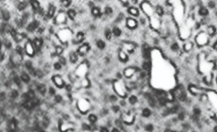
Figure 6: Magnified acoustic view of a small area shows that even tiny voids have bright centers.
Although the wet cleaning of silicon wafers between processing steps dates back to the beginnings of the industry, today’s advanced ICs including MEMS and flip chip devices can benefit from the latest plasma etchers designed to better eliminate residual contaminants.
By Suraiya Nafis, Head of Sales for Semiconductor Equipment for PVA TePla America
During the manufacture of integrated circuits (ICs), it is necessary to perform many deposition and etching steps to build the necessary internal structures; cleaning operations are common between wafer stops along processing lines. Among the most common are ‘ashing,’ or stripping, to remove photoresist from etched wafers, as well as ‘descum’ processes to remove any residue.
Although solvents can be used to remove photoresist in a wet process strategy, alternatives that allow for dry processing are often sought out due to reducing chemical handling and acquisition costs. Among the alternatives for dry processing are plasma tools that apply ionized energy for wafer ashing and descum.
Today’s plasma etchers are more advanced and automated, yet the tools have been available since the earliest days of the semiconductor industry. Since then, plasma processing has been expanded to include the removal of polymers, SU-8 and sacrificial layers. Plasma etching is also used for wafer cleaning, chip carrier cleaning, encapsulation and flip chip underfill as well as for wafer stress relief, chip side healing (CSH) and passivation for ultra-thin wafer technologies.
Given the maturity of the market and the refinement of processing techniques, plasma etchers – at least on the front-end – are relatively standardized, with fixed formats and off-the-shelf options. However, with the addition of more back-end applications along with the explosion of MEMs, microfluidic devices, power devices, HB-LED, PLED, and photovoltaics that utilize similar manufacturing techniques and tools, more semi-customized solutions are now required to adapt to the varying sizes, substrates and other challenges that manufacturers now face.

Plasma ashing and descum
Plasma ashing is the process of removing photoresist by ‘burning-off’ the organics. Using a processing tool, monatomic plasma is created by exposing oxygen or fluorine gas at a low pressure to high power radio waves, which ionize it. This process is performed under vacuum to create a plasma that turns the photoresist to ash.
Two forms of plasma ashing are typically performed on wafers. High temperature ashing, or stripping, is performed to remove as much photoresist as possible, while the ‘descum’ process removes residual photoresist. The main difference between the two processes is the temperature the wafer is exposed to while in an ashing chamber.
According to Suraiya Nafis, Head of Sales for Semiconductor Equipment for PVA TePla America, a leading system engineering firm that designs plasma systems, customers face a wide range of choices that include deciding between RF or microwave-based designs as well as the level of customization needed to address a particular manufacturer’s needs.
PVA TePla America specializes in advanced plasma systems and has an extensive history in the US, Europe and Asia dating back over 50 years. The company originally started out as International Plasma Corporation (ICP) and then later through acquisitions and mergers was known as Dionex, Gasonix, Metro Line and TePla.
As mentioned, high powered radio waves ionize oxygen or fluorine gas as essential steps of the wafer cleaning process. For photoresist removal, a critical decision equipment purchasers need to make is choosing between radio frequency (RF) or microwave-based units. When photoresist is removed, the underlying layers may be sensitive and could be damaged if the right choice is not made.
“Some devices are sensitive to plasma damage,” says Nafis. “If the device is not sensitive, you can use an RF generator, but if it is (sensitive) then you can use microwaves.”
In general, RF-based units are superior for stripping photoresist. RF plasma etches the surface through a physical process achieved by essentially bombarding the surface with plasma in a specific direction.
Microwave-based units, on the other hand, offer a ‘gentler’ approach because the plasma application does not have the same physical aspect to it, says Nafis. Instead, microwaves mainly deliver an isotropic chemical approach, which means it permeates everywhere. This also makes microwave units more ideal for removing material from the underside of flip chip devices that cannot be reached through direct physical bombardment.
Microwaves are also specifically useful for removing SU-8, a commonly used epoxy-based negative photoresist. When using a negative photoresist like SU-8, parts exposed to UV become polymerized, while the remainder of the film remains soluble and can be washed away. SU-8 was developed specifically to provide the high-resolution masks required for microfluidics, MEMs and other microelectronics applications.
“Among the many merits of SU-8 photoresist is its chemical stability, which can also make it difficult to remove,” explains Nafis.
As a result, Nafis says PVA TePla had to develop a process and technology that would remove SU-8
with dry plasma ashing. Microwave energy is used due to its isotropic etch property, which is also an advantage in removing sacrificial layers and to undercut the top layer. Another critical factor is more precise temperature control; in the past, plasma etchers often measured temperature, but provided little to no control. “The microwave plasma stripper must have very exact temperature controls because if the temperature is too high SU-8 becomes very hard and even more difficult to remove,” says Nafis.
In addition to choosing between RF and microwave-based systems, Nafis said that ashing and descum require different types of processing with one being more suitable to single wafer requirements while the other is best for batch processing.
Unlike photoresist stripping, descum is used to remove minute amounts of material in a more exact process. In doing so, it is important that critical dimensions of the wafer remain unaffected. This means that descum must be performed one wafer at a time.
“Descum, as a single wafer process, allows for more precise control compared to batch processing, and descum can still be performed at relatively high speeds.”
Plasma cleaning
When it comes to wafer processing, ashing and descum are essentially similar to cleaning. Both involve the removal of organic material. With this in mind, plasma is also used to remove particulates and other contaminates from glass and sapphire carrier wafers used to provide flat support during the manufacturing of ultra-thin silicon wafers.
During manufacturing, silicon and carrier wafers are temporarily bonded to facilitate downstream process steps. Once the process is complete, UV laser de-bonding separates the two substrates, leaving behind a silicon wafer just 50 microns thick. Because the glass and sapphire substrates can be expensive, cleaning and re-using them is ideal.
“Currently, cleaning carrier wafers is mostly done as a wet process using solvents, so it’s much more expensive and manufacturers have to dispose of the chemicals when they are done with them,” says Nafis. “It is much easier to clean carriers with dry processing using plasma since this will remove all the adhesive.”
Customisation
The ultimate lesson is that plasma tools are not one-size-fits-all, says Nafis. Each application will often have a very different set of requirements. However, because semiconductor manufacturing has so many fixed formats, some providers stick only to off-the-shelf options that provide little to no customization. “If you have anything that is not fixed format, it is a bit hard to get some suppliers to put in the engineering time,” he says.
For companies like PVA TePla that are willing to customize, the advantages to customers comes through their investment in research and development engineers, facilities and equipment to propose appropriate solutions. This includes being able to provide single wafer or batch processing systems, RF or microwave-based systems, various size chambers and solutions that range from manual to semi-automated to fully automated, high-speed production systems. Even details such as fixturing, types of loading/unloading systems, temperature controls and the ability to run multiple size wafers in a single system play a critical role.
“When a customer comes to us, they often don’t know which tool they need,” says Nafis. “So, we find out about the application and we can then suggest the tools that will work the best and fits within their budget.”
For more information, contact:
PVA TePla America
951-371-2500 or 800-527-5667
A newly-patented imec concept utilizes silicon photonics and thousands of tiny interferometers to reduce a Raman spectroscope to the size of a smartphone.
By Els Parton, Harrie Tilmans & Pol Van Dorpe
Raman Spectroscopy is a time-tested means to analyze the composition of materials using a portion of light reflected from a sample into the instrument. Today’s most commonly available, highly accurate Raman spectroscopes are desktop-sized and expensive; handheld versions suffer from performance limitations and are also costly. Unlike existing handheld spectroscopes, imec’s new concept exhibits the high optical throughput and spectral resolution of a desktop system, opening a whole new range of applications in which complex samples can be analyzed with a more affordable handheld device.
From medieval paintings to drugs
Raman spectroscopy was discovered by C. V. Raman in 1928, which earned him the Nobel Prize for Physics in 1930. Raman spectroscopy is used to identify materials – fluids, powders, solids – and to learn more about the materials composition. Today’s spectroscopes shine laser light on the material, and by analyzing a specific part of the scattered light, a spectral chart can be made. The scattered light that is analyzed is the so-called ‘Raman scatter,’ which is characterized by a different wavelength than the laser’s wavelength. It originates from the molecular vibrations in the material. One can recognize the spectral ‘fingerprint’ of each material and compound in the spectral chart.
Raman spectroscopy is used in many different fields – in fact, it can be used in any application where non-destructive material analysis is needed. For example: in pharmaceutics, Raman discloses the distribution of active compounds in medicinal tablets. Raman can also classify meteorites in chondrites and achondrites based on its mineral composition. It can even dive into the kind of hybridization in a (carbon) molecule and tell whether it’s a sp2 or sp3 hybridization. In semiconductor R&D, Raman spectroscopy can be used to determine the electrical properties and the number of layers of graphene, or characterize the stress in specific layers. In life sciences, Raman is able to tell something about the interaction between cells and specific drugs. In art work, the technique is used to identify which pigments were used, which in turn can give an indication about the artist’s identity, his working method, and the age of the work. Even the mummified skin of ‘Otzi the Alpine Iceman’ was examined with Raman spectroscopy.
-xr9om5.jpg)
Figure 1: Existing dispersive handheld spectrometers make use of entrance slits, mirrors, and gratings like those indicated in this scheme. In this way, the etendue and spectral resolution are coupled through the size of the entrance slit. Downscaling of the spectrometer leads to lower spectral resolution or acceptance etendue.
Numerous Raman spectroscopes are available today, specifically tuned to varied applications. Raman systems are often implemented as a microscope where the sample is illuminated with a diffraction limited spot and the Raman photons are collected with a high NA (numerical aperture) objective. Next to these desktop devices (which make up the largest part of the market), handheld counterparts have also emerged. These are really convenient for research ‘in the field’ like in the case of art work studies or archeology.
As is often the case with miniaturized versions of measuring equipment, handheld Raman spectroscopes are not as good as the desktop versions. For the study of the pigments in paintings, they work fine because the pigments generate strong Raman signals, but for more complex samples such as opaque fluids (such as milk), skin or powders, the current systems are not adequate or need a long measuring time. Also, the high pricing of handheld Raman spectroscopes inhibits widespread use.
What if a cheap but high performance handheld Raman spectroscope was available? Which new applications would be made possible? Think of food screening ‘on the go,’ skin screening for melanoma at the general practitioner’s office, or screening for drug authenticity by authorities throughout the supply chain. Within the food and beverage industry, it can be used for characterization purposes and for identifying and evaluating the authenticity, safety and quality attributes for a broad range of food and agricultural products. For instance, Raman is an ideal technique to identify and indicate the adulteration of edible oils or to determine the level of alcohol in beverages. Multiple component analysis using Raman spectroscopy is key (for example) in understanding the quality of milk by determining the fat, protein and water content of the milk a cow or a goat is producing (in real time). For cosmetics, Raman spectroscopy can be used for verification of the purity of ingredients such as those used in personalized moisturizing creams and essential oils (eucalyptus, ginger, lavender, basil, vanilla). Furthermore, it can be used to determine the remaining concentration of solvents in pharmaceutical preparations to decide if the level of nutrition is sufficient for a certain cell culture to maintain their growth.
-fjnxj.jpg)
Figure 2: Existing photonic-based handheld spectrometers are limited in miniaturization by the etendue of single-mode waveguides.
There are two main challenges in developing Raman systems. First of all, spontaneous Raman scattering is typically very weak, and as a result the main difficulty of Raman spectroscopy is separating the weak inelastically scattered light from the intense Rayleigh scattered laser light.
Secondly, in strongly scattering media, such as food or human tissue, the incident photons are not confined in a small spot, but instead generate a blurred spot, with sizes up to several millimeters. This increases the “optical throughput” or “etendue,” which is a measure for the spread of the light in space and angle. A spectrometer usually limits the etendue, which drops for compact devices.
In commonly used dispersive spectrometers, the light is focused on a slit, and its spectral components are separated using a diffraction grating. Miniaturization of a high spectral resolution device (<1 nm) requires a reduction in the slit width, thus reducing the etendue.
Ultimate miniaturization of optical devices can be realized using integrated photonics and waveguides. The etendue of a single-mode waveguide (which is the ultimate scaling of this approach) equals approximately l², with l the wavelength. If the used wavelengths is (for example) 860nm, this results in an etendue of 7.3e-7 mm²sr, which is 106-107 times lower than required for analyzing diffuse scattering samples.
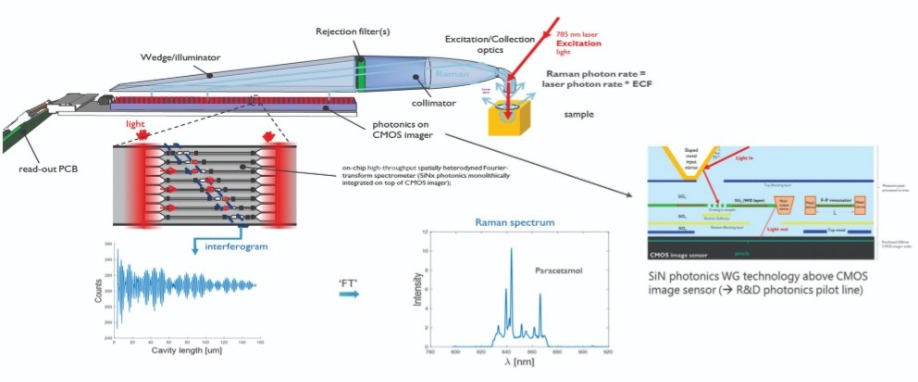
Figure 3: Concept of the patented solution made by imec researchers for a handheld Raman spectrometer, using a million interferometers on top of a CMOS image sensor. This build-up allows for extreme miniaturization without compromising on the etendue of the sample. This way, complex samples can also be measured. Furthermore, by using chip technology, the price of the device can be much lower than current devices.
Because of the limitations of current approaches in handheld Raman spectrometers, other concepts have been investigated. Another class of spectroscopy is based on light interference and implemented (for instance) in Fourier transform spectroscopy or in spatially heterodyne spectroscopy. These concepts exhibit an intrinsically larger etendue and are therefore more ‘scaling proof’.
A well-known Fourier Transform spectrometer is based on the Michelson interferometer. A beam of light is divided into two beams that take different paths before coming together and interfering. This enables tiny differences in the wavelength to be measured. The disadvantage of this design – particularly if you want to miniaturize it – is that two mirrors are used, one of which moves.
Researchers from imec have now developed an integrated photonics version of such a scheme without moving parts: the integrated spatially heterodyne spectrometer. The etendue is less limited in this case and equals n x l², with n being the number of interferometers. As mentioned above, if the used wavelength is (for example) 860 nm, and the preferred etendue (for complex samples) is around 0.5 mm²sr, then about a million interferometers would be needed.
This massive parallelization is possible with integrated photonics. The patented solution monolithically integrates close to a million interferometers on top of CMOS image sensors and light is delivered using micromirrors.
This is the working principle of the newly developed Raman spectrometer: Laser light (785nm wavelength) is focused on a sample and the scattered photons are collected and collimated by means of a compound parabolic concentrator (CPC). After filtering the Rayleigh photons (at 785nm), Raman photons are directed to the on-chip waveguide (WG) access ports using a wedge-shaped light guide and chip-integrated micromirrors. By a proper choice of the wedge shape and the angle of the incident light, the micromirrors are able to redirect the light with a large efficiency (>50%), where it is coupled into the WGs thru gratings linked to individual single mode WG interferometers. The interferometers exhibit a range of lengths, allowing for reconstruction of the original spectrum. Their outputs are aligned with the pixel pitch of the integrated CMOS image sensor serving as a highly parallelized detector array. The chip is wire-bonded to a PCB and connected to a custom designed read-out board to capture the data and transfer it to a computing device, which reconstructs the spectrum and displays the required property.

Figure 4: Part of the spectrometer chip layout, showing an evanescently coupled Fabry-Perot resonator (17.6µm long) together with the grating in-coupler(s) and the sloped output mirror for coupling the light to the pixels.
Due to requirements of CMOS compatibility and visible transparency, silicon nitride was chosen as the waveguide material. The WG stack is built monolithically on top of the BEOL of 200mm front side illuminated CMOS image sensor wafers. Post-processing is done in a 200mm CMOS pilot line, using 193nm DUV lithography for patterning the WGs and grating couplers.
The spectrometer chip is constructed using SiN-based waveguide photonics, implemented on top of a CMOS image sensor (CIS) used for electrical readout. The spectrometer chip as used in the current design consists of an array of massively parallel evanescently-coupled Fabry-Perot interferometers, varying in length in the range 2.2-152.8µm (in linear steps of 0.2µm). Incident light is coupled into the waveguide structures using a grating based in-coupler (GC). Sloped metal output mirrors are used to couple the light from the waveguide to the readout pixels of the CIS (see also insert with a cross-section of the chip in figure above). An illustration of the layout showing a top view of
the F-P resonators together with the grating in-coupler and sloped metal output mirror is shown in figure 4.
Conclusions
Raman spectroscopy is a powerful analytical technique with numerous applications. Existing desktop devices are rather bulky and have a price range of a few hundred thousand dollars/euros. The handheld solutions that exist today fail to reach the desired performance for high-end applications. Thanks to a new concept, it is now possible to overcome this performance barrier. By massive parallelization of waveguide interferometers integrated monolithically on top of a CMOS image sensor, both high optical throughput and high spectral resolution can be reached in a miniaturized device. This novel system is built in imec’s SiN biophotonics platform that guarantees robustness and compatibility with high-volume manufacturing.

About Els Parton
Els Parton received her engineering degree and PhD at the KU Leuven, Belgium. She joined imec in 2001 as a scientific editor. In addition to writing numerous articles on imec research, she is editor-in-chief of imec magazine, a digital magazine published every month. www.imecmagazine.com

About Harrie Tilmans
Harrie Tilmans received his PhD in Electrical Engineering from the University of Twente, The Netherlands. He has held R&D positions at the University of Twente, Boston University, the University of Wisconsin-Madison, Johnson Controls Inc (Milwaukee), the Catholic University of Leuven (Belgium), and CP Clare Inc (Hasselt, Belgium). His research covered MEMS resonators and resonating sensors, micro relays and RF-MEMS switches; MEMS and ultrasound transducer modeling and simulation, MEMS-CMOS process integration technology, MEMS packaging and assembly technology as well as integrated photonics. He has been with imec (Leuven, Belgium) since September 1999, first as Team Leader, then as imec Principal Scientist and Program Manager. He has managed and still manages several MEMS and photonics system based (industrial and funded) projects, more recently in the life sciences field. He has co-authored over 250 papers and issued over 20 patents. In 2001 he received the Eurosensors XV Fellow award for his pioneering work on microresonators.

About Pol Van Dorpe
Pol Van Dorpe received his PhD at the faculty of engineering of KU Leuven for his work in the field of spintronics. Afterwards he was appointed as a postdoctoral fellow of the FWO-Flanders (2006-2012), based in imec, and focused on metal based nanophotonics, or plasmonics for biosensors and energy harvesting. During this period he worked for some time at Stanford University and he established world-wide collaborations with renowned scientists in this field.
His work has led to over 140 peer-reviewed papers in high impact factor journals and has attracted more than 5000 citations. Since 2012 he has held a position as part-time associate professor at the physics department of KU Leuven; he is active as a principal member of staff in the life sciences department of imec where he leads a team working on experimental biophotonics. His main research focus is enabling novel applications in the life sciences field using integrated photonic concepts.
Part of the work was performed under the EU-funded IoSense project; the authors acknowledge the funding received from the Electronic Component Systems for European Leadership Joint Undertaking (ECSEL-JU) under grant agreement No 692480 (Project Acronym: IoSense). This Joint Undertaking receives support from the European Union’s Horizon 2020 research and innovation programme as well as Germany, The Netherlands, Spain, Austria, Belgium, and Slovakia.

