


Displacing an incumbent technology is never easy. But what helps to do this is a compelling story, clearly demonstrating that the new rival has the upper hand, and is the way forward.
When it comes to SiC, we now have a great story to tell. That’s because this March, Venturi, a Formula Electric team with a budget far smaller than many of its rivals, netted its first win with an all-SiC power module made by Rohm.
Venturi has been competing in this event for several seasons. When it started, it would finish near the back of the field, using cars equipped with all-silicon modules. In the season that followed, the car’s performance improved, thanks to the combination of silicon IGBTs and SiC diodes. But it is the pairing of SiC diodes and SiC MOSFETs that has propelled the team to podium finishes.
Many of the reasons behind this success are the traditional selling points for SiC. Alongside the superior efficiency, there is the opportunity to trim the size and weight of the module.
Just how big these savings are were disclosed in keynote presentation by Aly Mashaly, Director of Power Systems at Rohm Semiconductor (see the feature in this issue, Automotive market will drive further growth in SiC and GaN). For Venturi, the introduction of a smaller, lighter module was incredibly beneficial – it enabled this unit to be moved to the ideal location, where it enhances the handling of the car.
Traditionally, one of the strengths of motor sport is that the latest technology filters down into cars that you and I can buy. But when it comes to battery-powered cars with SiC modules, it’s already within our grasp. In the Model 3 Tesla, there is a SiC power module made by ST Microelectronics.
While Tesla is the best-known pioneer of the electric vehicle, it’s by no means the biggest investor. It has pumped in about $10 billion, compared with around $90 billion for Volkswagen, according to figures presented at CS International by Hong Lin, Senior Analyst from Yole Développement.
The competition that will follow this investment could be ferocious for Tesla. However, it is great news for all those working in the SiC industry. It will help to swell the growth of all forms of electric and hybrid electric vehicle, a sector that is going to be the primary driver of sales of SiC transistors and diodes for some time, and should increase global annual sales for this class of power device to around $5 billion within a few years.
The US Department of Energy's (DOE) Office of Energy Efficiency & Renewable Energy (EERE) has announced that twenty teams have moved onto the second round of the American-Made Solar Prize, a $3 million competition to revitalise US solar manufacturing.
Each team will receive a $50,000 cash prize and is eligible to compete in the next two phases of the competition. Through a rigorous evaluation process, teams were chosen for the novelty of their ideas and how their solutions address a critical need for the solar industry. The innovations represented by the competitors include advances in photovoltaic and concentrating solar-thermal power technologies, new power electronics devices, and innovative manufacturing techniques.
Projects include: 'High-Capacity 250 Kilowatt SiC Solar String Inverter' from a power electronics startup based in Boulder, CO; 'Three-port SiC-based High Frequency Power Conversion System' from a Milwaukee team; 'Acoustic Cleaving of GaAs for Next Generation PV' from researchers at Arizona university who aim to create a new manufacturing method that can lower the cost of high efficiency photovoltaic materials; and 'Perovskite + Silicon Tandem Product Prototype' by a Californian start-up based.
“We are impressed by the caliber of ideas submitted by competitors,” said Daniel Simmons, Assistant Secretary for the Office of Energy Efficiency and Renewable Energy (EERE). “These teams represent the next frontier for solar innovation and we're excited to see the teams work with our partners in the American-Made Network and at NREL to make these ideas a reality. In the end, the best ideas and collaborators will win.”
The teams will tackle a variety of solar challenges, including the development of new PV cell designs that can increase efficiency and improve manufacturability, new devices like inverters that use low-cost SiC or tools that ease PV installation, and new hardware and module designs that enable new applications for PV.
The teams from 15 states will work to design a proof of concept over the next three months. Competitors will then pitch their work to a team of expert judges at a national demonstration day in May. Then, five to ten finalists will compete for two final prizes at a second demonstration day this fall.
Shareholders of II-VI and Finisar have voted to approve proposals related to II-VI's acquisition of Finisar. Both companies received enthusiastic shareholder support for the proposals related to the merger agreement first announced on November 9, 2018.
97 percent of the shares of II-VI common stock voting at II-VI's special meeting voted to approve the proposal to issue shares of II-VI common stock pursuant to the merger agreement, and 99 percent of the shares of Finisar common stock voting at Finisar's special meeting voted to approve the proposal to adopt the merger agreement.
The combination of the two companies would form a formidable photonics and compound semiconductor company capable of serving the broad set of fast growing markets of communications, consumer electronics, military, industrial processing lasers, automotive semiconductor equipment and life sciences. Together, II-VI and Finisar employ over 24,000 associates in 70 locations worldwide upon closing of the transaction.
“Since the merger announcement, our shareholders have gained an appreciation of the long-term value creation that the unique breadth and depth of this combination will enable,” said Vincent D. Mattera, Jr president and CEO, II-VI Incorporated. “Meanwhile, the feedback from our major customers in the communications and consumer markets continues to be overwhelmingly positive, due to the high complementarity of our enabling technology, intellectual property, product portfolios and global footprint.”
“While the two companies continue to operate independently, the integration teams are working together to ensure a seamless integration and transition,” said Michael Hurlston, Finisar's CEO. “We see the positive overlap between our cultures, the mutual appreciation for our companies' capabilities, the exceptional synergy potential, and the energizing outlook for our future.”
The merger is expected to be completed in the middle of calendar year 2019. The merger filing is under review in China by the State Administration for Market Regulation (SAMR), in Mexico by the Federal Economic Competition Commission, and in Romania by the Romanian Competition Council.
Raytheon's GaN-based next generation Enterprise Air Surveillance Radar (EASR) - the newest sensor in the US Navy's SPY-6 family of radars - has begun live testing.
EASR has already completed subsystem testing at Raytheon's Near Field Range in Sudbury, Massachusetts. More recently, the 6 foot x 6 foot rotating array was wrapped, loaded onto a flatbed truck and eventually crane-lifted onto a 100 foot test tower at the Surface Combat Systems Centre at Wallops Island, Virginia. Once up and running, the radar will undergo system-level testing, tracking a variety of aircraft through the end of 2019.
The GaN-based Enterprise Air Surveillance Radar, or EASR, is the US Navy's next generation radar for aircraft carriers and amphibious warfare ships, providing simultaneous anti-air and anti-surface warfare, electronic protection and air traffic control capabilities.
"Going from 'cold steel' to a fully calibrated radar in less than one year is no small feat, but that's exactly what we accomplished with EASR," said US Navy Captain Jason Hall, program manager for Above Water Sensors, Program Executive Office Integrated Warfare Systems. "The scalable building block architecture developed for AN/SPY-6(V)1 enabled EASR to rapidly complete subsystem testing. We are making great strides toward delivering SPY-6 capability across the fleet."
Raytheon is building two variants of EASR: a single-face rotating array designated AN/SPY-6(V)2 for amphibious assault ships and Nimitz class carriers, and a three fixed-face array designated AN/SPY-6(V)3 for Ford class aircraft carriers and the future FFG(X) guided missile frigates.
Both versions of EASR are built on scalable Radar Modular Assembly technology as well as a software baseline that has been matured through development and recent test successes of AN/SPY-6(V)1 the US Navy's program of record for the DDG 51 Flight III destroyers. Each RMA is a self-contained radar in a 2 foot square box. These individual radars can integrate together to form arrays of various sizes to address any mission on any ship. EASR also adds air traffic control and weather capabilities to the mature SPY-6 software baseline.
Upon completion of system-level testing in Q4 2019, EASR will shift from the engineering and manufacturing development phase to the production phase. The 1st delivery of AN/SPY-6(V)2 to LHA-8, the America Class Amphibious Assault Ship, is on plan for 2021.
GaN Systems, has announced a strategic partnership with Aveox, a provider of mission critical electro-mechanical power solutions, to significantly reduce the size and weight of the company's 3-phase AC power converters with Active Power Factor Correction (APFC).
This partnership enables the development of power-dense, Aerospace-Compliant power conversion modules for a wide variety of cockpit, galley and cabin equipment that use 3 Phase power.
Aveox's high-efficiency power conversion modules for aerospace and defence systems are designed to replace legacy Transformer Rectifier Units (TRUs) around the world. GaN Systems says its power devices allow the modules to be more than five times smaller than conventional units using silicon technology.
GaN switches have very low losses which enable an efficiency of >97 percent, significantly reducing the amount of heat generated. Using compact GaNpx bottom-cooled devices, Aveox was able to combine both the semiconductor switches and surface-mounted magnetics onto a single Insulated Metal Substrate (IMS) board, making the converter smaller than before possible.
"Running GaN Systems devices at high frequency has enabled us to significantly reduce the size and weight of our newest generation power conversion modules, said David Palombo, CEO of Aveox Inc. Together with GaN Systems, we are excited to see our advanced technologies enable leading aerospace companies to develop some of the world's most efficient and lightest weight power systems for safety critical applications."
"We are excited to be working with leading companies like Aveox and seeing the growing number of innovative, state-of-the-art GaN-based products released in the market, especially in industries where durability and reliability count," said Jim Witham, CEO of GaN Systems."With this partnership, we are seeing how GaN Systems is playing a pivotal role in providing an innovative energy-efficient solution. Most noticeably, there is a significant amount of momentum in various markets, as more companies realise the outcomes with GaN to enable smaller, lower cost, energy-efficient power systems."
VisIC Technologies, a GaN power semiconductor device company, has announced the availability of its On-Board-Charger (OBC) reference design for the fast-growing Electrical Vehicle (EV) market.
The 6.7kW OBC features a size and weight of only 2.3L and 4.5kg respectively, providing close to 3kW/L power density and proving the disruptive capability of GaN switches. This is 3 x better power density compared to commercially available products today. With the efficiency above 96 percent across a wide load range, it helps automotive manufacturers to reduce power losses and enables faster charging for electric car owners.
The 6.7kW OBC using VisIC GaN power devices targets plug-in hybrid vehicles/electric vehicles (PHEV/EV) applications. With a universal 110‐220V/16-32A AC input and 200‐430V DC output for charging the automotive battery by controlling voltage and current flow to the battery. The charger is designed to provide the interfaces to charging standards on the input power side and thus adapts to charging infrastructure.
The OBC design which uses VisIC's GaN technology, designed for Automotive qualification requirements AEC-Q101, demonstrates reduction in power losses, size and weight. The overall advantages include simplifying the cooling systems, reducing the charging time and reducing the size and cost of the EV.
"We are happy to release this OBC reference-design to help our customers to accelerate the design cycle and bring the best-in-class xEV chargers using VisIC's GaN technology to the market in a fast and efficient way," says Ran Soffer, VisIC's SVP sales and marketing. "This reference design proves the benefits and improvements VisIC's GaN technology can bring to the xEV users. With VisIC's GaN technology, electrical cars will be more efficient, lighter in weight and more affordable."
Semiconductor equipment manufacturer ClassOne Technology has sold its Solstice S4 system to Philips Photonics, one of the industry's leading providers of VCSEL devices. The announcement was made by Byron Exarcos, ClassOne Group CEO, and Hans Peter Ehweiner, general manager at Philips Photonics. The new ClassOne equipment will be installed at the Philips facility in Ulm, Germany.
“We will be using the new Solstice S4 for wafer cleaning applications,” said Ehweiner. “So, its unique processing flexibility and high performance are especially useful to us, as well as its small footprint. ClassOne's responsiveness and support for us in Germany are also significant factors in this purchase decision, thus we are looking forward to a fruitful and longstanding relationship."
"Solstice initially built its reputation on quality electroplating," said Exarcos. "But with its Plating-Plus capabilities, Solstice is now recognised as a powerful multiprocessing tool that can handle everything from plating to wafer cleaning, high-pressure metal lift-off, resist strip, UBM etch and more. Phillips Photonics is a perfect example of next-generation fabs that are using Solstice primarily for those additional wet processes. It's also notable that Solstice is becoming the tool of choice for VCSEL manufacturers around the world.”
The Solstice family of wet-processing tools includes the four-chamber Solstice S4 and the eight-chamber Solstice S8, for 75wph, automated wet-processing production, as well as the 2-chamber Solstice LT for semi-automated process development. The platform was specifically designed for ≤200mm wafers, which are used in compound semiconductor and many emerging technologies. With its special Plating-Plus multi-processing capability, Solstice is able to reduce the number of different tools that many users need to purchase. Solstice equipment is also known for being priced significantly lower than similarly configured systems from the large manufacturers. It has been described as providing “Advanced Wet Processing for the Rest of Us.”
With 20 years of history in VCSEL technology, Philips Photonics produces VCSEL-based solutions for data communications, consumer and industrial applications — for security, surveillance, night vision and a range of sensing applications. The company has enabled the introduction of laser-based PC mice, high bit-rate active optical cables, and has introduced VCSEL-based Laser Doppler Technology to consumer applications.

Rohm has announced the addition of ten new automotive SiC MOSFETs. The company says that the introduction of the SCT3xxxxxHR series means it now offers the industry's largest lineup of AEC-Q101 qualified SiC MOSFETs that provide the high reliability necessary for automotive on-board chargers and DC/DC converters.
In recent years an increasing number of automotive makers are offering electric vehicles in response to growing environmental awareness and rising fuel costs. However, although EVs are becoming more widespread, their relatively short driving range remains problematic. To improve driving distance, batteries are trending towards larger battery capacities with shorter charging times. This, in turn, demands high power and efficiency on board chargers such as 11kW and 22kW, leading to increased adoption of SiC MOSFETs. In addition, higher voltage batteries (800V) require power devices featuring low loss and higher withstand voltages.
To meet these needs, Rohm added ten new models to its lineup of AEC-Q101 qualified MOSFETs that uses a trench gate structure. The result is the industry's largest portfolio, available in both 650V and 1200V variants. And going forward, Rohm will strive to further improve quality and strengthen its lineup to increase device performance, reduce power consumption, and achieve smaller size.
In December 2010 Rohm was the first in the world to succeed in mass producing SiC MOSFETs. Rohm established automotive-grade quality and began supplying SiC Schottky barrier diodes for on board chargers in 2012 and SiC MOSFETs for DC/DC converters and on-board chargers from 2017.
Lumileds has introduced the Luxeon MultiColor Module 0.5W, a module that produces the highest luminous intensity of reds, greens and blues with what is claimed to be the industry's most consistent colour.
The module comprises a 3-in-1 RGB in a standard 3535 PLCC6 package. The module produces red light of 1,000 mcd, green light of 2,300 mcd and blue light of 500 mcd at 20 mA drive current (typical Vf of 2,1, 2.8 and 3.0V, respectively).
Reliability is said to be a key differentiator for the Luxeon MultiColor Module 0.5W. Testing in hydrogen sulphide environment reveals superior maintenance of flux and forward voltage of the red, green and blue LEDs.
“Long term performance in the application depends on a robust, reliable package design and in this arena, Lumileds stands alone,” said Jennifer Holland, product line director of Lumileds. The compact module features a black matte surface, a flat light-emitting surface and water resistant design (IPX8 rating), for use in a number of video wall and illumination applications.
Plessey has developed its proprietary 2D planar GaN-on-Si process to emit Green light without the need for colour conversion techniques.
To produce Green light, LED manufacturers typically apply phosphors or quantum dot conversion materials to native Blue LEDs. These materials then convert short wavelength, typically 450nm, Blue light to Red or Green wavelengths with typically 10 percent to 30 percent efficiency.
Plessey's native Green LEDs are formed inherently using its proprietary GaN-on-Si epitaxial growth process similar to the native Blue LEDs with the principal difference coming in the amount of indium that is incorporated in the quantum well structures of the LED.
With no colour conversion losses, the native Green emission is orders of magnitude times brighter than colour converted process for microLEDs. With a dominant Green wavelength of 530nm and a full width half maximum wavelength of 31nm the Green is well suited for colour displays. Additionally, the Green emission exhibits outstanding wavelength stability versus current density.
“Plessey already provides powerful, efficient native Blue microLEDs and through this innovation in our growth technology, Plessey has produced world leading high performance native green micro LEDs which will provide for next generation display and illuminator devices for our customers.” said Mike Snaith, chief operating Officer at Plessey.
Veeco has announced that Aledia, a Grenoble-based developer and manufacturer of next-generation 3D LEDs for display applications, has expanded its portfolio of Veeco thin film process equipment to support the development and production of advanced 3D micro-LEDs.
Aledia cited Veeco's proven leadership in compound semiconductor applications, GaN-on-silicon growth performance, and capability to grow a full range of high-quality epitaxial films as key factors influencing its decision.
“We have been impressed with the performance of Veeco's Propel GaN MOCVD platform for large-wafer 3D LED production, and naturally turned to Veeco again to support our advanced LED development,” said Philippe Gilet, co-founder and CTO of Aledia. “Veeco's solutions meet our rigorous material quality and system delivery requirements along with unmatched material flux stability and repeatability. We are excited to take the next step with them in producing next-generation 3D micro-LEDs.”
The collaboration between Aledia and Veeco reflects the immense promise of micro-LEDs and other advanced LEDs for the future of displays. Micro-LEDs offer high efficiency, brightness and reliability benefits with shorter response time, enabling lighter, thinner and flexible displays with energy saving advantages for applications such as wearables, smartphones, automotive, signage/large TVs, augmented reality/virtual reality, etc. According to a recent Yole Développement report, there have been close to 1,500 patents filed related to micro-LED display from 125 different companies, with the bulk of activity occurring after 2012.
“With the significant shift toward exploration of micro-LEDs for use in next-generation displays, leaders like Aledia are turning to Veeco,” said Gerry Blumenstock, senior vice president and general manager of Veeco's compound semiconductor business unit. “Veeco's proven materials engineering expertise puts us in a unique position to offer innovative thin film deposition technologies for customers tackling tough compound semiconductor research, development and production challenges.”
From here on in, Cree will focus on growing Wolfspeed with capacity increases in SiC production being a priority.

As Cree sells its lighting business, chief executive, Gregg Lowe, tells Compound Semiconductor, what will happen next.
Just last month, Cree revealed it is selling its underperforming Lighting Products business unit to Ideal Industries. The divestiture follows efforts – spearheaded by chief executive Gregg Lowe - to expand production at Wolfspeed and looks set to drive growth across the coming years.
“This gives us the cash to invest in Wolfspeed and establishes us as a pure-play compound semiconductor company focusing on SiC and GaN,” Lowe tells Compound Semiconductor.
“The cash will help to fund capacity expansions, including our manufacturing footprint and also our research and development resources.”
“Lighting Products was a completely different channel to market and added complexity to our business,” he adds. “But when you have the entire management team and board-of-directors focused on being a pure-play compound semiconductor business, this really allows you to double down and re-invest.”
Indeed, since joining Cree in September 2017, Lowe has single-mindedly worked on bolstering Wolfspeed, having grown the business by more than 100 percent.
Key moves include the acquisition of Infineon’s RF business and also several long-term SiC supply deals worth more than $500 million, including agreements with ST Microelectronics and Infineon.
“We set out to quadruple Wolfspeed revenues to $850 million by 2022 and now this [sale] really helps with that,” highlights Lowe. “We have a faster growth profile, higher margins and a cash balance approaching $1 billion.”
What’s more, Lowe is adamant that the power and RF focus comes at just the right time. As he points out, thanks to the rapid rollout of 4G and 5G networks, the demand for Cree’s GaN-on-SiC RF products is rising.
“This turned on quite quickly over the last two quarters so we’re trying to expand capacity very quickly here,” he says. “Of course our Infineon business acquisition here helped us to get a good foot in that market.”
And at the same time, car manufacturer investments in electric vehicles are increasingly gathering momentum. “Since I joined Cree, around $300 billion of investments have been announced and this is really driving the demand for silicon carbide.”
So what happens now? Lowe is certain that the Lighting Products divestiture works for every party involved. Ideal Industries gains a ‘good platform’ to expand its presence in Lighting and Industrial applications. And as he adds: “It’s a win for employees in the Lighting business as this will now be the largest division in Ideal and the main focus of this company.”
But clearly for the chief executive, Wolfspeed is the priority. Indeed, in past months Cree has been shifting research and development, crystal growth equipment and capital expenditure from its lighting arm to Wolfspeed, more than doubling capacity along the way.
As Lowe emphasises, cash influx from the latest sale will further grow manufacturing capacity, but Cree continues to talk with potential new SiC suppliers. Given this, more supply deals akin to those of ST Microelectronics and Infineon could well follow.
Meanwhile, in a similar vein to his Infineon RF and power business deal, the chief executive isn’t adverse to future mergers and acquisition. Describing these as ‘part of Cree’s ‘toolkit’, he says: “Whatever we do, we will be focused on growing the Wolfspeed business, and if there is a good merger and acquisition opportunity... well we have used that before.”
Importantly, Lowe also intends to plough more cash into research and development, to develop baseline technologies including SiC crystal growth, wafer fabrication and epitaxy capacities, which as he says will further increase yields and drive down costs.
“We will also cover device developments, applications engineering and field application resources as customers start to transition from silicon to silicon carbide power devices,” he says. “There are some application differences we will need to help customers work through and now we can fund these as well.”
And looking to the future, Lowe believes that higher-voltage devices will provide ‘interesting application opportunities’. As he highlights, Cree has demonstrated 20 kV devices, but believes that 650 V devices and those rated a little higher than that will continue to hold the company’s attention.
“The 650 V to 2000 V range is probably the vast majority of the market that we will be going after,” he says. “We want to convert the industry from silicon to silicon carbide and this means expanding our product portfolio, expanding customer reach and enabling new markets to make this transition.”
With its 1700 V SiC power module delivered, Rohm is eyeing even higher voltage markets and industry domination, reports Rebecca Pool
Be it for photovoltaics, electric vehicles, 5G infrastructure or industrial high-power supplies, SiC is steadily infiltrating markets around the globe. As analysts forecast a compound annual growth rate of at least 25 percent, and a $1.5 billion SiC market come 2023, industry players up and down the supply chain are readying for action.
US-based GT Advanced Technologies recently opened a SiC crystal growth facility to meet the imminent SiC market boom while Infineon has bought SiC wafer-splitting process developer, Silectra, to secure substrate supply.
Wolfspeed, Infineon, GeneSiC and more are diligently pioneering packaging structures to take on the extreme switching speeds and temperatures that SiC can handle. And in a bold move, Cree has sold its Lighting business to focus on power semiconductors, having spent the last year-and-a-half year bolstering its SiC supply and honing devices.
Amongst these front-runners is Japan-based Rohm, having had its eyes firmly fixed on SiC for some two decades. Preliminary SiC MOSFET development began in 2002, with initial samples shipped in 2005. Trial manufacture of 300A MOSFETs followed in 2007 with trench-type devices released in 2008.
Then, in 2009, the company acquired SiC crystal manufacturer, SiCrystal, with the now vertically integrated business delivering its first mass-produced SiC Schottky diodes and MOSFETs in 2010. Mass-produced full SiC modules followed in 2012 with Schottky barrier diodes on 6-inch wafers delivered in 2017.
Today, the company claims to have the industry’s largest line-up of automotive-grade 650 V and 1200 V SiC MOSFETs, but is also intent on delivering devices at ever-higher voltages for more and more gruelling applications. As Aly Mashaly, Power Systems Manager at Rohm highlights, the industry trend towards higher power density has led to higher systems voltages. And, given this, the company recently developed a 1700 V, 250 A rated SiC power module that is currently being used in customer projects.
According to Mashaly, the module’s high voltage surpasses the requirements of electric hybrid vehicles, for now, but is instrumental in inverted and converter applications for outdoor power-generation systems and industrial high-power supplies.
Crucially, the latest system promises to provide the same energy-saving performance as 1200 V devices with a high reliability, meaning the 1700 V SiC module is ready to take on the 1700 V silicon IGBT module.
“The big challenge in silicon carbide is to provide high reliability, especially at higher voltages,” says Mashaly. “But we have tested our devices at high voltages, temperatures up to 85 °C and high humidities, and for more than 1000 hours, and we haven’t seen any degradation in performance.”
The module comprises SiC MOSFETs and Schottky barrier diodes, vastly diminishing chip area and reducing on-resistance by 10 percent relative to similar SiC products, says Mashaly. But while this cuts energy use and heat dissipation, it doesn’t cut upfront costs, a fact that the Power Systems Manager knows only too well.
“We are working to reduce the level of the price compared to the IGBT [module], and while I cannot provide exact numbers, I do know that we will always be getting closer,” he says. “I don’t ever expect the cost of the SiC module to come down to that of the IGBT module but if we look at system cost , the benefits of using SiC has already been proven to many tier one companies and automotive OEMs.”
So with the demand for SiC power devices rising, how exactly is Rohm meeting market needs? While the company is in the process of ongoing capacity expansion at its Nuremberg site, in June 2018 it revealed plans to massively expand SiC production capacity at its Apollo plant in Chikugo, Japan. Construction has now started and will continue until at least the end of 2020.
At the same time, the transfer of manufacturing from 4-inch to 6-inch wafers is also well underway, boosting production efficiencies. “We have already started this for our planar MOSFETs and this year we will try to make this transition with our trench MOSFETs,” says Mashaly.
What’s more, Mashaly reckons that the wafer quality of Rohm’s 6-inch wafers is better than that of its 4-inch wafers. “We have nineteen years of experience in SiC and we saw a huge improvement in the quality of [our] four-inch wafers compared to two-inch wafers, and we now see that quality is even better with the six-inch wafers,” he says. “Year by year we have this improvement in our production process and we are confident that the quality in the next level of substrate will be high.”
So with manufacturing in hand, where next for Rohm on the road to SiC success in an increasingly crowded market-place? Mashaly is keen to highlight that aside from Wolfspeed, Rohm is the only vertically integrated business in this market, and as such, intends to capture 30 percent market-share by 2025, making it the number one player.
And as well as an ever-larger market share, the company will also be looking towards ever-higher voltages. “Right now we are focusing on the 1200 V and 1700 V areas due to the big potential for mass production of SiC here,” he says. “But we already have research and development activities in place for 3.3 and 6.5 kV [devices]... we don’t have a defined time when we will launch these products but we also see the potential for SiC here.”

“We have nineteen years of experience in SiC and we saw a huge improvement in the quality of [our] four inch wafers compared to two inch wafers, and we now see that quality is even better with the six-inch wafers”
Monitoring electron diffraction with artificial intelligence promises to boost epiwafer production yields
BY Young-Kyun NOH FROM IVWorks
We are in the midst of the Fourth Industrial Revolution. Innovation in manufacturing is underway, thanks to integration of conventional production and network connectivity with the Internet of Things (IoT) and Artificial Intelligence (AI). The benefit of this is that it enables AI manufacturing – that is, the use of production processes that are managed through intelligent machines, systems, and networks that autonomously sense and analyse information.
The adoption of AI and IoT is already driving big changes within a range of industries. Armed with AI, manufacturing processes can be monitored in real-time through the sensing, collecting, and analysing of sensor data using IoT. This capability allows the swift identification and resolution of problems in manufacturing facilities, leading to enhanced productivity. Ultimately, it will enable many tasks to be transferred from human engineers to AI systems, and create a seamless manufacturing environment.
At IVWorks, a GaN epiwafer foundry start-up headquartered in Daejeon, South Korea, we are moving with the times. We have developed and applied a deep learning-based AI epitaxy platform, known as Domm, that dramatically improves the productivity and scalability of MBE-grown epiwafers. This patented technology, which uses a deep learning algorithm to detect and analysis electron diffraction patterns, monitors crystal growth at the atomic level in real time.
Today, we are using our Domm platform on three MBE systems that produce 100 mm to 200 mm GaN epiwafers for DC and RF power devices. We monitor the electron diffraction pattern with a deep learning algorithm, and information about the entire crystal structure of the epiwafer is classified and converted into data. If abnormal patterns are identified, an alarm is raised with the engineer. This level of adoption of AI is referred to as Level 2 (see Figure 1 for an overview of the different levels).
This is just the start of our venture into AI. In February 2019, we closed a $6.1 million series B funding round that will enable us to expand our manufacturing capabilities and upgrade the Domm platform to higher levels (see Figure 2 for our roadmap). The first step will be a move to Level 3, the AI Assistance level. Here, data acquired through the deep learning algorithm is learned by correlating it with the quality data of the produced epiwafers. This allows the probability of pass/fail to be intelligently predicted in real time, assisting the engineer.
Further ahead, we will move to Level 4 and then on to Level 5. The lower of these is known as the AI Production level. This bolsters yield by automatically revising the process conditions of the recipe in real time, according to the predicted probability of pass/fail. When operating at Level 5, known as the AI Manufacturing level, it is possible for AI to develop a customized epiwafer recipe of a new structure. To accomplish this, epiwafer quality results, according to recipes, are accumulated and learned. In addition, correlations are established, and their validity analysed.
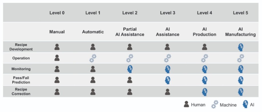
Figure 1. Various levels for IVWorks Domm platform.
The need for AI
The use of AI makes a dramatic impact on MBE, due to the complexity of this growth process. Successful growth of epiwafers demands strict control of many conditions, including: the substrate temperature; the temperature distribution of the substrate and the reactor; the internal pressure inside the reactor; the number of source atoms; the relative ratio between the sources; the growth rate; the size and geometry of the reactor; the flow pattern and the flux pattern of the source; and atomic migration (or diffusion), which includes binding reactions on a substrate surface. To illustrate this complexity, just consider the growth of a 3 µm-thick GaN FET epiwafer. It is formed by depositing approximately 12,000 or more atomic layers, each added with precisely controlled conditions (see Figure 3).
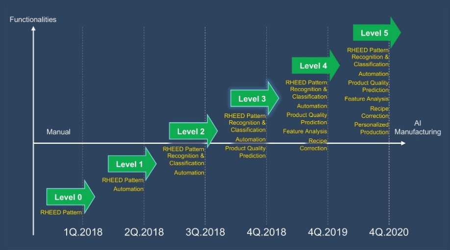
Figure 2. Roadmap for IVWorks Domm platform.
The conventional approach to managing productivity is for an engineer to collect and analyse data related to the epitaxial growth process conditions, the equipment status, and the results associated with the quality of the manufactured epiwafers. However, comprehensive analysis of the epi-structure and the process are challenging, and this can lead to variations in the analysis of the collected data, depending on the expertise of the engineer. When the collected data is difficult to quantify, variations are exacerbated, compromising the reliability of the results of the analysis, and ultimately hampering efforts to control and monitor the epiwafer manufacturing process. Since limits on human resources often cause bottlenecks in productivity and scalability, there is a great demand for a highly advanced, automated solution that is efficient, convenient, and capable of a real-time, seamless response that maximises the manufacturing productivity of the epiwafers.
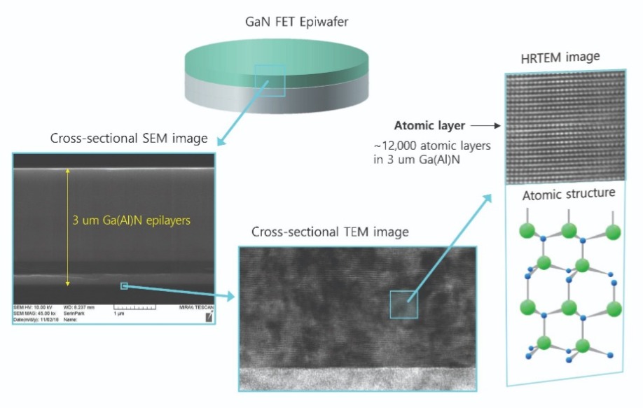
Figure 3. The epiwafer is single crystalline semiconductor wafer upon which complex structures, comprising many individual atomic layers, are deposited.
To develop automated solutions that maximise epiwafer manufacturing productivity, it is critical to employ quantitative monitoring of both the process state of the equipment and the growth state of the epi-structure. Given that the focus has to be on maximising the yield of products and managing the manufacturing process to ensure that the material is as close as it can be to the target characteristics, process conditions should be ideally corrected in real-time during epitaxial growth. And if that’s not possible, the recipe must be updated after every growth.
Automation of the monitoring process requires the collection of monitoring data that has high validity and a high degree of correlation. Options for monitoring epitaxial growth in today’s commercial reactors include thermocouples, infrared temperature sensors, pressure gauges, residual gas analysers, optical-based flux monitoring tools, and gas flow monitors. If insight is required into either the growth state of the epi-structure, the growth rate or the wafer curvature, measurements and monitoring can be provided with reflectometer and deflectometer methods.
However, note that for the manufacturing of epiwafers, with the techniques just listed, quantitative automated monitoring is yet to be applied that identifies the crystal growth modes and the crystal structure formation at the atomic level. This knowledge is important, as it can determine the characteristics of epiwafers. Fortunately, it can be determined during MBE growth, which takes place under vacuum, using reflection high-energy electron diffraction (RHEED). This form of electron diffraction can reveal crystal quality, crystal composition, crystal growth rate, and V/III flux ratios in real time with atomic layer resolution. To do this, an electron beam is directed onto the surface of a substrate under crystal growth, and the reflected electron diffraction pattern is analysed.

One of the great strengths of RHEED is that it offers real-time, direct measurements of the crystal growth state that are highly correlated with the quality of the epiwafers. However, as the measured data is in the form of an image of the diffraction pattern (see Figure 4), its interpretation requires an engineer with expertise. Even then, the engineer can only undertake simple numerical analysis or empirical analysis to gain an insight into the crystal growth. It is difficult to quickly interpret various diffraction patterns, so when an engineer uses the technique, it is confined to R&D, and not applied to production. That’s partly because a large amount of data is obtained on each atomic layer, and as there are thousands to tens of thousands of them in an epiwafer, an overwhelming amount of data is created.
The good news is that these limitations can be overcome with AI image analysis technology and big data technology. In fact, this pairing is so powerful that it is highly likely to exceed the interpretation ability of any human engineer.
Historically, AI image analysis has been a two-step process. Initially, engineers extract the main features of the objects for modelling and design, before AI and big data takes over, detecting and analysing objects. For example, for a cat in an image, engineers pick out features, including two pointed ears, as well as the arrangement of the nose tip, the forehead, and the chin within certain angles on a round face. They then sophisticatedly model and input this type of information for detection and analysis.
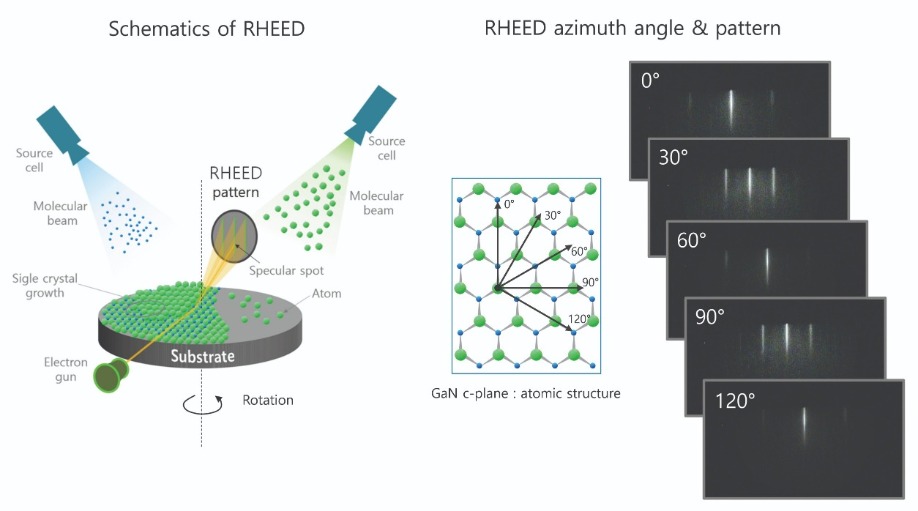
Figure 4. Real-time monitoring of the surface atomic structure during the epitaxial growth.
Recently, however, AI has moved on. Now a machine can distinguish objects in images by training, using just data itself, rather than requiring preliminary work from an engineer. The machines of today can distinguish objects in a new image by learning validity and correlation of the images on the database – they don’t need information on the actual object (see Figure 5).
This AI algorithm, called ‘deep learning’, is a major breakthrough for classifying and interpreting RHEED measurements. It allow systems to monitor, in real time, the crystal characteristics for every atomic layer in entire epistructures.
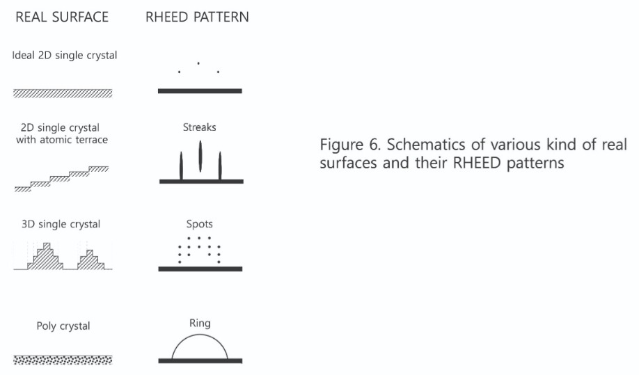
With RHEED patterns, the surface crystal structure of an epiwafer is captured by the shape of an electron diffraction pattern. For example, streaky patterns represent two-dimensional growth, those that are spotty signify three-dimensional growth, and rings reveal polycrystalline growth. Within all these patterns, there are details of crystal structure characteristics, captured in the degree, spacing, and brightness of each pattern (Figure 6).
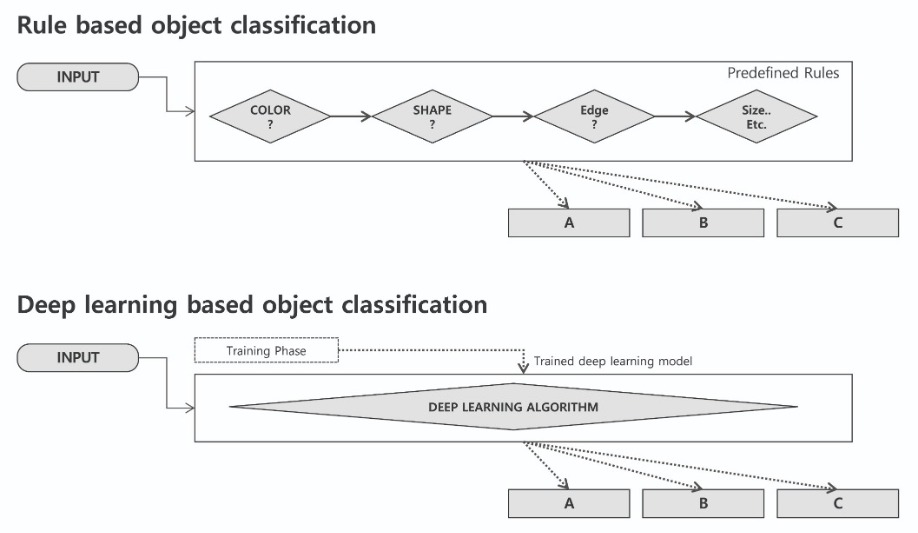
Figure 5. A comparison of conventional and deep learning methods of image classification.
Using our Domm platform we can create a prediction model. It is formed by learning the validity and correlation of the dataset that integrates the classified RHEED patterns, growth conditions, and the quality results of the epiwafers. We can apply this prediction model to epiwafer manufacturing to maximise productivity (see Figure 8).
During the production of GaN-on-silicon FET epiwafers with a basic structure, our Domm system collects RHEED pattern images at up to 30 frames per second, from the beginning to the end of epiwafer growth. Commencing with thermal deoxidation on the silicon surface, and on to the growth of the AlN seed layer, the GaN buffer layer, the AlGaN barrier, and SiN passivation, our system detects and classifies the shape of the diffraction pattern for each atomic layer, along with the transition of patterns. Our model is capable of accomplishing this, thanks to training through deep learning for the entire structure. As a result, Domm monitors and intelligently analyses the manufacturing process, in addition to collecting data on growth conditions and equipment status, and determining pass/fail results.
It is challenging to determine the crystal structures of the GaN buffer layer and the GaN/AlGaN heterojunction interface. However, we are able to gain insight into this by monitoring the setting conditions – including substrate temperature, shutter sequence, and source cell temperature – and the patterns produced by the surface of the wafers, the deoxidation process, and the seed layer. What’s more, by quantitatively measuring pattern transition during the formation of the interfaces surrounding each layer, we are able to quantify the level of similarity with the manufacturing of pass products. When these results are used to predict yield in real time, or sub-standard quality, this can boost productivity, either by requesting a correction to the engineer or by automatically correcting the recipe (see Figure 9).
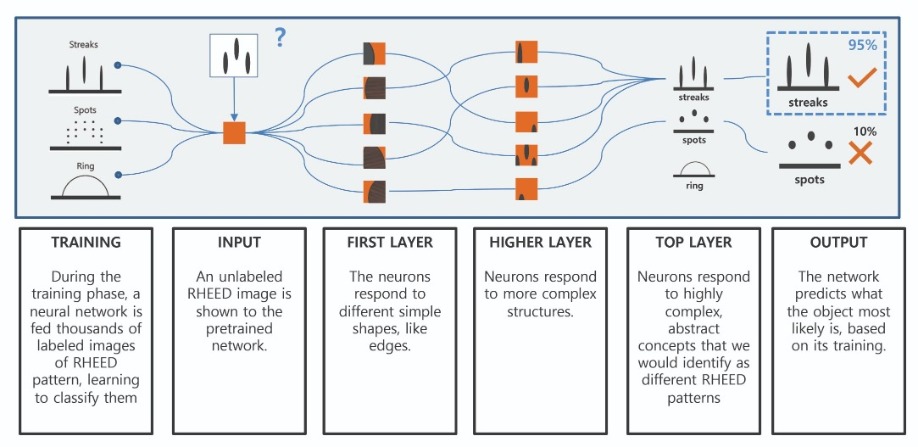
Figure 7. RHEED pattern recognition using a deep neural network.
As compound semiconductor manufacturing involves a number of different, complex processes that are conducted step-by-step, this hampers the construction of effective, high-quality input datasets needed for AI. But this could start to change, now that we are demonstrating that RHEED patterns can offer high-quality input data that ultimately provides the highest level of resolution for semiconductor crystal structures.
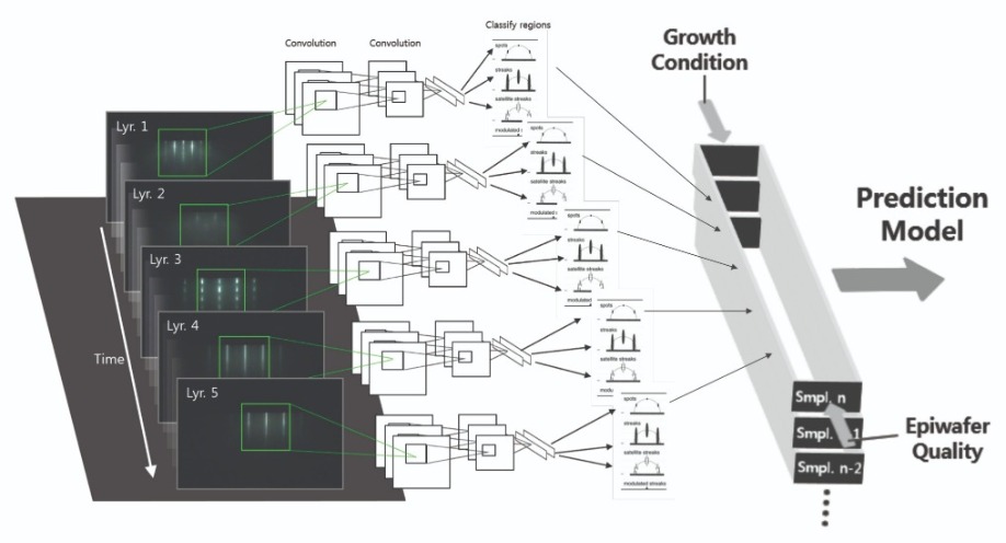
Figure 8. IVWorks patented AI epitaxy platform Domm.
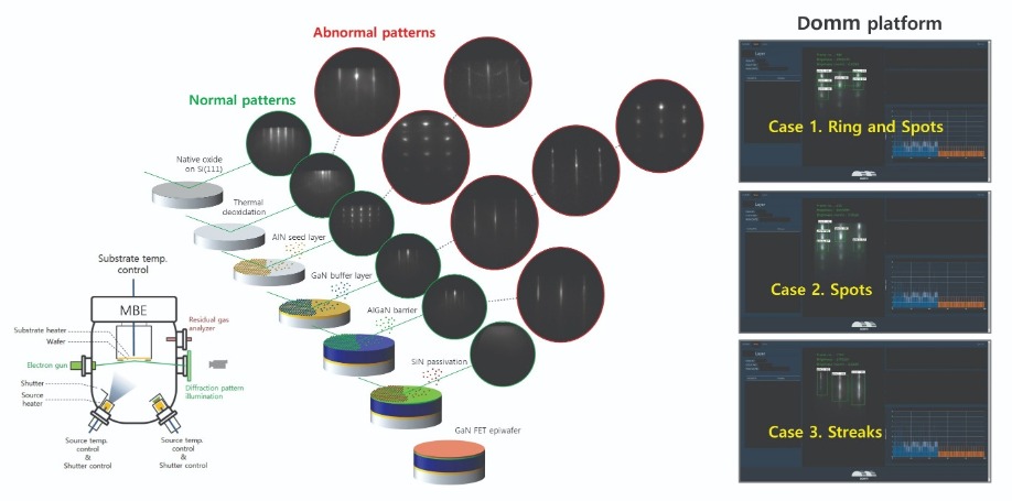
Figure 9. RHEED pattern detection and classification by Domm platform.
W. Braun, 1999. Applied RHEED : Reflection High-Energy Electron Diffraction During Crystal Growth. Springer, Berlin, NY.
A. Krizhevsky et al. 2012. Conf. Advances in Neural Information Processing Systems : ImageNet Classification with Deep Convolutional Neural Networks.
S. Hasegawa, 2012. Characterization of Materials: Reflection High-Energy Electron Diffraction. John Wiley & Sons, Inc.
Revenues will rocket to several billion dollars, thanks to a ramp in sales to the automotive sector
BY RICHARD STEVENSON
A great way to strengthen the case for a new technology is to highlight how much better it is than the incumbent. That’s the strategy that has been pursued by the pioneers of wide bandgap power devices. For many years, they have been demonstrating the significant energy savings resulting from more efficient power conversion, and the beneficial implications, including a trimming of electricity bills and an increase in the deliverable output from solar panels.
Right now, however, this industry has a new, even better story to tell –and one that is sure to capture the public imagination. It stars an underdog in the form of Venturi, a racing team that has a far smaller budget than many of its rivals. Off the pace for several seasons, it has been improving of late, and this March it caused an upset by netting its first win in the Formula Electric class. What’s is the secret to this success? The adoption of a new, superior technology, in the form of an all-SiC power module produced by Rohm.
Details of this winning module and the benefits that it delivers were discussed by Aly Mashaly, Director of Power Systems at Rohm Semiconductor, during a keynote presentation at this year’s CS International. At this meeting, held in Brussels on 26-27 March, Mashaly revealed that the benefits of using SiC, rather than silicon, were not confined to just delivering greater power from the battery. Instead, they extend to a 30 percent decrease in the size of the unit, as well as a reduction in its weight, which fell from 15 kg to just 9 kg. These improvements, which stem from the opportunity to use smaller passive components, are incredibly valuable – they allow the module to be placed in the ideal spot within the car, leading to better handling.
Venturi’s foray into SiC power electronics is relatively new. Back in season two (2014-2015), it employed an all-silicon module in its Formula E car. In season three, this evolved to the pairing of a silicon IGBT and a SiC diode, and from season four onwards, it has used the combination of SiC diodes and SiC MOSFETs.
Initially, Venturi’s cars were equipped with a 200kW inverter, operating at a 16kHz switching frequency. Replacing the silicon electronics with SiC enabled an increase in switching frequency to 24kHz, for an inverter producing an output of 220kW. Efficiency at the maximum power increased by more than 1.3 percent, and the maximum efficiency went up by 1.1 percent. However, these figures fail to show the true benefit of the switch to SiC. During racing, cars operate at a variety of loads – and at a partial load, the efficiency with SiC power electronics is more than 5 percent higher than it is with silicon.
The strengths of SiC will benefit not just racing cars, but all electric vehicles. Mashaly explained that for a car with a 33kWhr battery, switching to superior electronics can extend the driving distance – evaluated in terms of a reduction in battery charge from 100 percent to 10 percent – from 159 km to 177 km. Alternatively, a smaller battery can provide the same driving range. Given the high cost of the battery, this can lead to a reduction in total expenditure.
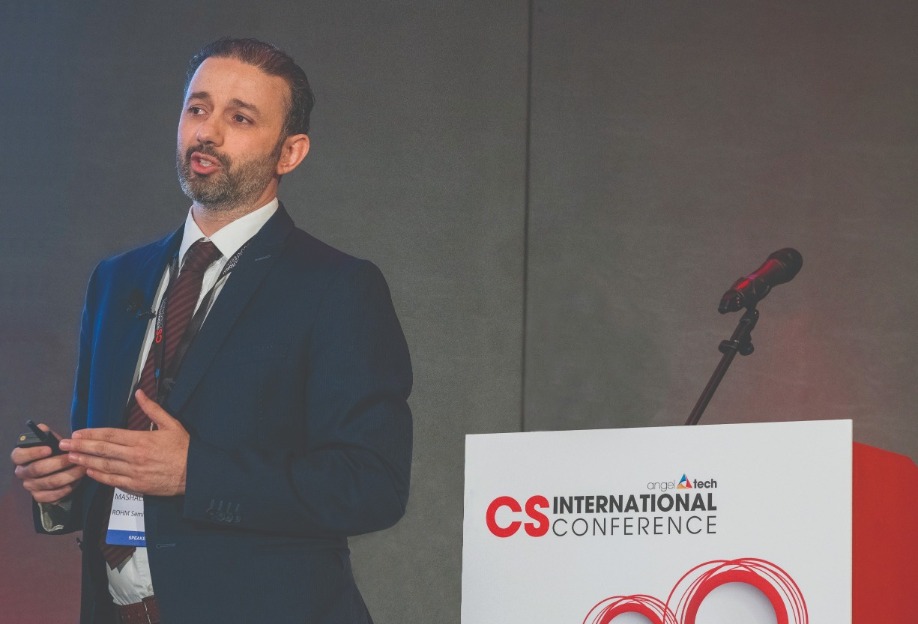
Aly Mashaly, Director of Power Systems at Rohm Semiconductor, gave a keynote presentation at CS International detailing the benefits of replacing silicon with SiC in the power module of a Formula Electric racing car.
Delegates gained further insight into the growing markets for wide bandgap power electronics, along with advances related to device design and production, in many other talks given at CS International. They included an insight into the electric and hybrid electric vehicle market by Hong Lin, Senior Analyst at Yole Développement.
Her analysis, which shows that where the substantial investment in electric and hybrid electric vehicles is coming from, will raise a few eyebrows. While Tesla is grabbing headlines, it is by no means making the biggest investment in this technology. According to Lin, Elon Musk’s firm has invested around $10 billion, while Volkswagen has devoted nearly ten times that to develop this technology. That substantial sum is helping Europe to lead the way, investing $150 billion, compared with $107 billion for Asia and just $39 billion for the US. Lin explained that sales of electric and hybrid electric vehicles will rocket over the next few years. She revealed that they hit 5.8 million last year, are tipped to climb to more than 10 million by 2020, and will exceed 25 million in 2024. Growth will occur in all forms of vehicle – mild hybrids, full hybrids, plug-in hybrids and battery-powered electric vehicles.
There are opportunities for wide bandgap power electronics in the DC-to-DC converters, the main inverter, the generator, and the on-board battery converter. According to Lin, switching from silicon to SiC devices could boost the battery voltage from 400V to 800V, and enable an increase in the driving range.
In mild hybrids, electronics convert the 12V output from the battery to 48V, which is used for the likes of air-conditioning, the brakes, and electric power steering. This task is a “perfect target for GaN”, argued Lin.
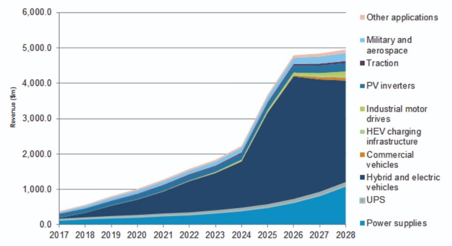
IHS Markit is expecting the SiC market to grow substantially, due to greater deployment of this wide bandgap material in electric vehicles.
A view on where all the markets for SiC and GaN power devices stand today, and what can be expected over the next few years, came from Richard Eden, a Principal Analyst at IHS Markit. Projections provided by him suggest that the global revenue for SiC totalled about $0.5 billion in 2018, will double by 2020, and then climb to almost $5 billion by 2026. In comparison, worldwide sales for GaN power devices will net around $150 million this year, and will rocket to $1.8 billion by 2028.
Two significant markets for SiC devices are photovoltatic inverters – after early success deployment of SiC fell, but it is rising again – and power-factor-correction in power suppliers. But both these sectors will be far smaller than that for electric and hybrid electric vehicles, which will take the lion’s share in the coming years.
Eden does not expect SiC to make a significant impact in either traction, industrial motor drives or wind turbines. Current handling is the issue in all these applications. “You need hundreds of amps, not tens of amps,” argued Eden.
A major concern within the SiC market is the supply of material. Although many substrate supplies have entered the market, including Dow DuPont, II-VI Advanced Materials, Norstel, Showa Denko and Sumitomo, Eden believes more are needed. Wolfspeed still dominates, with material in such high demand that Infineon Technologies and STMicroelectronics have recently negotiated supply agreements to guarantee substrate supply.
Eden noted that there has been a shift from 4-inch to 6-inch substrates, a move that was hoped to reduce costs by around 50 percent. However, this promise has not been fulfilled, due to a fall in yield.
Device results for SiC are encouraging. There are now trillions of hours of device field experience available, and data suggests that SiC diodes and transistors do not have reliability issues. What’s more, the manufacturers of these devices are meeting JEDEC and automotive AEC-Q101 standards.
Another advance is the expansion of the SiC portfolio. There are launches of SiC MOSFETs and JFETs operating at lower voltages, such as 900 V, 800 V and even 650 V. This shift enables SiC MOSFETs to go head-to-head with silicon super-junction MOSFETs with identical voltage ratings.
Dynamics in the wafer and epiwafer markets for GaN are very different from those in the SiC industry. The majority of GaN power devices are grown on silicon, so substrate supply is not an issue. Those that are making these devices can draw on the services of epiwafer providers, but that’s uncommon, says Eden. Instead, most the of production by IDMs and by foundry services involves in-house epitaxy.
The majority of GaN-on-silicon production is on 6-inch wafers, with volume ramping slowly, while 8-inch GaN-on-silicon is yet to take off. Alternative foundations for GaN are failing to make much headway, according to Eden. Although growth on bulk GaN is being aided by the reduction in the price of the substrates, due to the collapse of the laser diode market, interest in this approach has taken a knock, due to the collapse of Avogy, the premier pioneer of this technology. Meanwhile, other alternatives – sapphire, SiC and ceramic wafers, such as that made by Qromis – are known to offer performance benefits, but they are perceived to be unnecessarily expensive compared with GaN-on-silicon.
When it comes to devices, GaN transistors are now in mass production, being deployed in server and telecom power supplies, and also in power adapters and chargers. Automotive systems suppliers are also looking at this technology, which is being considered for on-board chargers and DC-DC converters.
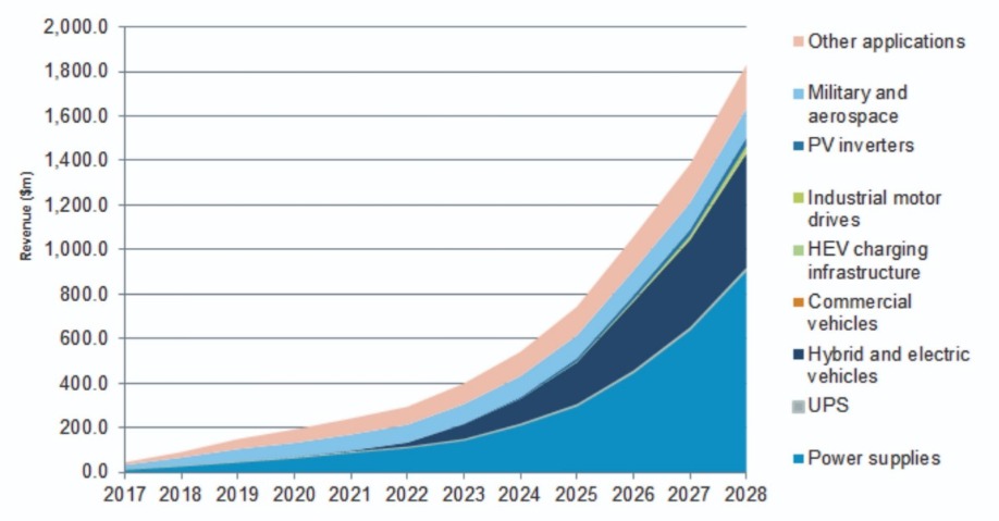
According to IHS Markit, the global GaN device market will take off over the next decade.
One option for increasing the capability and commercial impact of GaN power technology is to unite it with silicon CMOS. At X-Fab, they have been developing processes to do just this, which were detailed in a presentation given by project manager Ralf Lerner.
Lerner argued that the benefits of GaN and CMOS integration include: reductions in interconnect distances and losses, leading to improved performance; a smaller form factor; a trimming of power consumption; and lower costs.
According to Lerner, there are two types of approach for this form of integration. One is monolithic. However, when this is performed on CMOS, the challenge is to address the incompatibilities in materials and thermal budgets; and when this is undertaken on GaN, the resulting technology is held back by being restricted to simple logic, and a lack of GaN PMOS. The alternative, heterogenous integration, can be accomplished by either direct wafer bonding, which is impaired by restrictions on chip size and wafer diameter – or by micro-transfer printing, the approach adopted by X-Fab.
Engineers at this fab start with a densely packed source wafer, and use an elastomeric stamp to transfer arrays of dispersed devices to a target wafer. Etching silicon beneath the transistor aids the removal of the devices, with a fast pick-up providing high adhesion, and a slow release producing weak adhesion that assists the printing process. On-wafer metallisation completes heterogeneous integration.
Measurements on transistors with a 17 µm gate-drain spacing, made using devices with an epitaxial thickness of just 5 µm, produce a drain current of just 1 µA at 1800 V. According to Lerner, the breakdown is primarily determined by the lateral gate-to-drain spacing, rather than the buffer thickness.
There are drawback with this printing approach. Yield depends on more factors than it would do for a conventional approach, as it is influenced by the quality of the source wafer, the target wafer, and the printing yield. There is also a trade-off between printing costs and material losses. However, this printing approach also has many merits. Lerner pointed out that: it allows for optimised processes for CMOS and GaN; it offers flexibility in chip and wafer dimensions; and it realises a low ohmic metallisation at the wafer-level, which aids heat spreading.
Boosting blocking voltages
For blocking voltages of 1 kV or more, the leading rival to silicon is SiC. But GaN can also operate in this domain, thanks to a variety of advances in GaN-on-silicon technology. These include improvements to epitaxial growth and selective removal of silicon. Both options were discussed by Farid Medjdoub in a keynote presentation.
Medjoub began his talk by championing the lateral GaN device, which is the more common architecture. He argued that its merits include the highest electron mobilities and the best cost-to-performance ratio.
The challenge to realising a higher blocking voltage, such as 1 kV or more, is the need for a thicker buffer layer, which can increase wafer bow and defect density, while compromising reliability.
Carbon-free buffers, produced by drawing on expertise at Allos Semiconductors, address all these issues. For a 6.6 µm-thick buffer featuring several interlayers, GaN-on-silicon epiwafers have a concave bow of just 23 µm, while trapping of carriers in the material is low all the way up to 1 kV. “The vertical breakdown voltage is 1400 V, which is state-of-the-art,” said Medjdoub.
He has also evaluated material from EpiGaN, which has a total thickness of just 5 µm. Using a reference buffer that has been optimised for 650 V applications, measurements on the heterostructure reveal very low trapping up to 1.2 kV. “This is another example that 1200 V is reachable with GaN-on-silicon,” argued Medjdoub.
Even higher voltages are possible with selective substrate removal. Values of 3 kV have been reached by first removing the silicon below the buffer layer, before adding a 15 µm-thick film of AlN by PVD, followed by a 2 µm-thick film of copper. Medjdoub and his co-workers are now working with
ON Semiconductor to apply this approach to industrial devices that are 4 mm-wide, normally-off, and capable of delivering a current of 10 A or more. Testing shows low trapping up to 3 kV, indicating that the silicon replacement does not induce additional trapping effects.

Hong Lin, a Senior Analyst at Yole Développement, predicts that sales of electric and hybrid electric vehicles will climb to more than 10 million by 2020 and to over 25 million in 2024. Growth, which will spur sales of SiC and GaN devices, will occur in all forms of vehicle – mild hybrids, full hybrids, plug-in hybrids and battery-powered electric vehicles.
Advantages of AI
During the production of power devices, epiwafers are inspected for quality control. It is usual to use bright field, dark field and differential interference contrast to identify and categorise defects on the surface. But what about buried imperfections?
According to Shivanui Lyer, a solutions architect at Nanotronics, these can be exposed by ultra-violet photoluminescence. In her presentation she showed a wide range of defects, exposed by ultra-violet photoluminescence with different excitation wavelengths.
Classifying defects is time-consuming and tricky, and the use of artificial intelligence promises to streamline and improve this process. Nanotronics have taken this approach, investigating the capabilities of artificial intelligence and comparing the results with those obtained with an operator. When they discovered a discrepancy, further investigation revealed human error. “We were thrilled. We had achieved super-human results,” remarked Lyer.
Superior SiC substrates
With demand for SiC substrates at a high, it is important that this industry obtains a high yield from every wafer, to ensure as many high-quality devices as possible get to market.
One way to do this, argued Revasum’s CTO, Robert Rhoades, is to use single-wafer processing, along with robotic handling. He claimed that compared to a batch approach, this enables a higher degree of precision, increased reliability, and ultimately a boost in yield. “Yield is key,” argued Rhoades. “It trumps other concerns.”
Revasum’s single-wafer tools are used to polish substrates. They employ a grinding approach, with a fixed abrasive. This is said to lead to far less sub-surface damage to the substrate than the batch-based lapping approach, which employs loose abrasive and creates more sub-surface damage. Note that the removal of material is far faster with grinding, so the throughput of the multi-wafer tool is not as significant as one might expect.
Another benefit of the single-wafer process is that during the polishing process, the slurry and debris, described by Rhoades as being like “microscopic concrete”, is less likely to adhere to the substrate. This means that with a batch approach, the slurry and debris might dry on the wafer during unloading, a situation that does not occur with single wafers, which benefit from a wet-in, wet-out process.
Getting the best out of every substrate is essential right now. Demand for SiC transistors and diodes is increasing, and must be fulfilled with high-quality products to support further growth in the market. With GaN, it’s a slightly different story.
Here, sales are smaller, but again a great future awaits. To find out just how good it will be, and get an update on the progress of all wide bandgap devices, make sure you attend next year’s CS International.
Founded just a year ago, WaferChina is on a mission to become a substantial supplier compound semiconductor epiwafers to the domestic market. Richard Stevenson catches up with its CEO, Ping Gong, who outlines the growing markets for its products, manufacturing challenges, and the company’s expansion plans
Q: What are the long-term goals for WaferChina?
A: The long-term goal is to make WaferChina the number one VCSEL epiwafer supplier in China. China is very heavily reliant on importing epiwafers.
Q: Your company is focusing on GaAs-based optoelectronic materials, and in particular, VCSELs. Why does the world need another supplier of epiwafers for GaAs-based VCSELs?
A: Right now, there are new opportunities. People are talking about AI and 5G. These new technologies are coming to your life and my life. With these new technologies, you need a lot of semiconductor lasers and detectors. Smart cars are coming, smart phones have been on the market for years, and I believe this is almost a revolutionary time for changes in industry, in terms of the car, the phone, and homes.
For this you need a lot of semiconductor chips and wafers. In China, there are some chip companies that are growing, but there is a lack of epi-companies. The chip companies are very heavily relying on the importing of epiwafers. So there is an opportunity in China for domestic epi-wafer suppliers.
Q: What do you see as the biggest markets for the GaAs VCSEL?
A: The biggest market is for commercial electronics – for instance, the phone application. The Apple brand has brought the VCSEL into bigger market production. I see this as opening the door for applications of VCSELs in 3D applications.
Datacoms are a stable market for VCSELs, and are growing steadily, as they have been over the last decade. But I think the market will be much smaller than that for 3D applications.
Q: Who are the biggest VCSEL makers, in terms of devices? And do they tend to outsource the epi, do this in house, or a combination of both?
A: Right now, Apple’s supplier is Lumentum. Lumentum largely relies on IQE’s epiwafers. It has some R&D activity, in terms of epi, but not mass production, from what I understand.
There are some other companies, like II-VI. They have in-house epi, and they are making chips themselves. They are more integrated. Also, there is Finisar. They are pretty integrated.
There is a relatively new VCSEL player AMS. They have invested a lot in the last two or three years, in terms of VCSELs. They acquired Princeton Photonics, so a fabless company with expertise in designing. They have set up their own manufacturing in Singapore with MOCVD reactors and a chip production line with 6-inch wafers. But as far as I know, they are still in the ramping up stage in terms of epi and not in mass production yet.
Q: How big is the VCSEL epiwafer market, in terms of the number of wafers per year?
A: From my understanding, the current market is about 50,000 6-inch wafers. That many is consumed by one phone company. With Android systems coming up now, I believe that number will go up very quickly.
Q: You are based in ShaanXi Optoelectronic Incubation Centre. Is that a supportive location for your venture?
A: The biggest benefit of the incubation centre is that it helps the company to start very quickly. Our MOCVD tools moved in at the end of March and the beginning of April 2018. We started sampling from July 2018. So that was a really fast start.
The incubation centre doesn’t give any cash support, but it gives facility support. It has a cleanroom, and some equipment. Our company has only bought MOCVD reactors and some characterisation equipment.
Q: Tell me about the very early days of the company. Where did the idea come from, and how did it get off the ground?
A: The motivation for me to set up the company is the VCSEL market taking off. I have been involved in VCSEL epitaxy over the years, and the market has never been big enough. But from two years’ ago, when Apple had this face recognition application, the VCSEL became a really hot product. I realised that there are huge opportunities, so I decided to set up this company to do this business.
In China there are no volume VCSEL epi-wafer suppliers. And the market is huge. In the phone market, China is 60 percent of the world. The car industry is also very big. So there are lots of opportunities in China.
Q: How long can you stay in the incubation centre?
A: There is no time limit, but capacity is limited. The cleanroom can have up to eight-to-ten big MOCVD reactors. So before we grow any bigger than that, we can stay there. But eventually we will have our own production site.
Q: Who are the investors in the company? And do you get much support from the government?
A: We are a pure commercial company. We are a joint-venture between British and Chinese. We started with two local VC investors, and we have had another round of funding. Currently, we have four venture-capital investors.
Q: Will you need to find more investors to grow the company? Or could that come from re-investing profits?
A: After two rounds of funding we have now bought enough MOCVD tools. We will have to see what the market is going to do over the next couple of years. If we need to expand faster, we may have to raise more money. But if we have a more regular expansion, we can probably use our own cash flow. It’s not a problem to raise more money. There are many investors that are interested in investing in us.
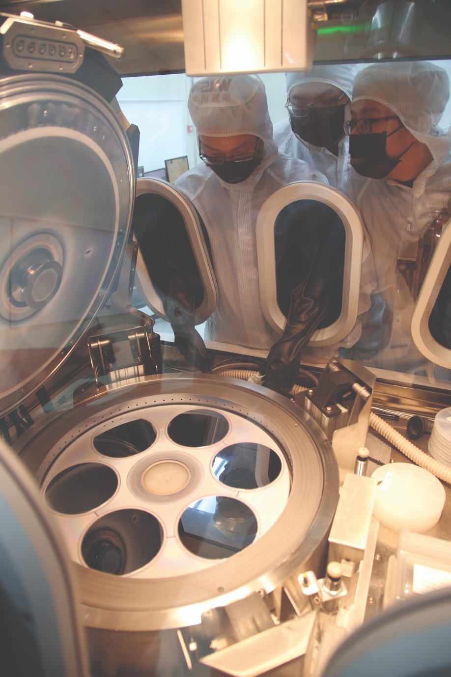
With the arrival of two more MOCVD machines in the second quarter of this year, WaferChina will have the capacity to produce more than 20,000 6-inch wafers per year.
A: We have under twenty employees right now. But we also have some engineers supporting us from the incubator centre. They provide general support, like running the facilities and gases.
I have an operations director, Qiang Zhang. He has twenty years of experience of working in silicon IC fabs. He is good with cost control and quality control. He is helping to set up the WaferChina quality system and operation
system.
Recently Andreas Eisenbach has joined our technical team. Eisenbach has 30 years’ experience in III-V compound semiconductor epitaxy, R&D, production and product management.
Q: How much capital equipment have you bought?
A: Currently, we have three MOCVD production reactors. We have ordered two more, which are coming in April 2019, which will take us up to five reactors.
The incubator centre has a lot of characterisation equipment. We have only bought some very specialised equipment.
Q: What is the capacity of your fab?
A: With the additional two reactors, we could produce more than 20,000 6-inch wafers per year. We can produce 3-inch to 6-inch epiwafers.
Q: How do you characterise your epiwafers?
A: It depends on the product. For the VCSEL we provide PL mapping, reflectance uniformity and PL wavelength data, doping characterisation and surface morphology.
For the edge-emitters, we also provide thickness data, doping data, composition data, uniformity, and PL wavelength, of course.
Q: The VCSEL is a relatively complex structure. Your company faces strong competition from the likes of IQE, that have many years of experience in making these products. How can you compete with all that experience?
A: I think that most of the IP is in the customer design. From an epitaxy material-quality point-in-view, I’m confident with our team’s more than fifity years of experience in working in the MOCVD epitaxy industry – that there are a lot of fundamental things that our team understand very well. We believe we can grow very good quality material.
Of course, a big company like IQE has its own expertise. But their major advantage, in my opinion, is mature production.
In comparison, we are more competent in terms of lead time and technical services to Chinese local customers. The flexibility of lead time and technical support is particularly important for new markets like the VCSEL. We are developing products together with our customers.
Q: Do you think it’s easier to grow VCSELs now than 20 years ago, due to improvements in MOCVD tools?
A: I would say the reactor performance has improved, but fundamentally, there is still a need for a lot of experience, especially in trouble-shooting. Let me put it this way: run-to-run uniformity is a lot better than it was twenty years ago, but from time to time there is still a shift in quality, or in uniformity. So troubleshooting, understanding the process, is still critical.
Q: Are you able to hire talented process engineers with expertise in VCSEL epiwafer growth?
A: Most of our engineers are from the LED industry. They have been trained up over the last ten months, and they are getting more competent in terms of understanding VCSEL growth. The major technology has come from our technical team’s experience.
Q: As well as a good a MOCVD reactor, high-quality metal-organics are crucial to VCSEL quality. Do you think Chinese companies are capable of producing these materials with sufficient quality, or will you be sourcing from an international supplier, such as your former employer Azko Nobel?
A: It’s not just metal-organic sources, but arsenic and phosphine. Now we can use 60 to 70 percent that is domestically produced. But there are some key materials that we are still importing, like from Azko Nobel, for critical layer growth.
Q: Are there IP issues surrounding the growth of the VCSEL? And how do they impact you?
A: I think most IP is in the epi structure design, which is with our customers. In terms of epitaxy process, I don’t think that there are too many restrictions. Basically, epitaxy is hands-on processing, and there is a lot of individual experience and trouble-shooting skills needed. Of course, we do respect IP, international law and Chinese law. The company has to be very sure we don’t run into any problems with that.
Q: Do you expect a high proportion of your sales to be domestic? Or will much of your revenue come from overseas?
A: I think the majority of sales will be domestic business, because there will be a big demand in China for VCSELs, as well as other lasers and detectors, and there is not much commercial VCSEL epiwafer supply in China. Especially with the current phone and car applications, China will be a big market, in terms of epiwafer demand. Our goal is to be world-class on the domestic market.
Of course there is no reason why we cannot sell products outside China.
Q: Does the current US-China trade war hamper international sales, but aid domestic sales?
A: I think that domestic sales may be positively impacted, because of the taxation. If you want a wafer from the US, currently you have to pay 25 percent tax. But for exporting, as far as I know, there is no tax added on. So there should not be much impact for our international sales.
The current trade war is between China and the US, and the two governments are working on a solution very actively, I believe. They will reach an agreement.
Q: Have you started to sell epiwafers?
A: Yes, we have gone through the sampling stage.
Right now we have customers buying product from us. They have gone through the qualification stage. But the volume is not big yet, because most of our customers are start-up companies, and they need to take time to qualify their customers, and develop their products.
Q: What are the goals for the rest of this year?
A: We will hopefully get into a mass production stage by late 2019, after our customers go through their qualification with their customers, the cell phone companies.
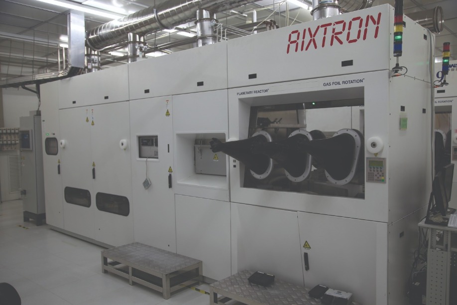
WaferChina has three MOCVD reactors for its growth of GaAs and InP epiwafers. Two more tools will be installed in the second quarter of 2019 at its facility in the ShaanXi Optoelectronic Incubation Centre.

CEO and founder of WaferChina
CEO of WaferChina, Ping Gong, founded the company in April 2018. Prior to embarking on this venture, he worked for AkzoNobel for more than 12 years, initially as Marketing Manager for the Asia Pacific region, and more recently as the Global Technical Development Manager. Between 1998 and 2005 Gong held the role of Senior MOCVD Growth Engineer and then Project Manager at IQE, Cardiff. During his time at IQE, he was responsible for the production of epiwafers for various lasers, including several types of VCSEL. He holds a PhD in Optoelectronic Materials from The Chinese Academy of Sciences, and a Bachelor’s degree in Semiconductor Devices from Xidian University, China.
A novel ion-implantation technique improves the manufacture of SiC power devices, including super-junction MOSFETs
BY Michael Rueb FROM MI2-FACTORY
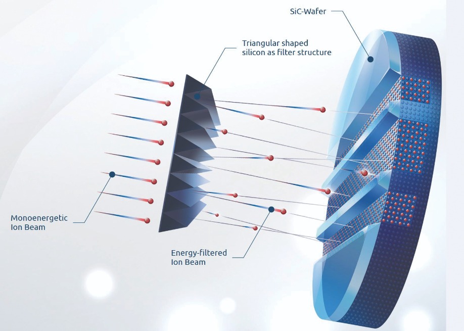
In the run-up to the turn of the millennium, a silent revolution took place in the silicon power electronics industry. Back then, the on-resistance of commercial transistors plummeted by a factor of between three and ten, thanks to the introduction of a superjunction architecture in unipolar, high-voltage devices. To create this device, a super-junction is formed by creating p-type, high-aspect-ratio columns in n-doped vertical drift zones (see Figure 1).
Today, the super-junction is a cornerstone of the silicon power industry. It features in Infineon’s CoolMOS, ST-Microelectronics MD-Mesh, Fuji’s Super J MOS series, ON Semiconductor’s Super FET and Toshiba’s DTMOS. This class of devices, which is tending to operate in the 500 V to 900 V range, is serving in switched-mode power supplies in phones, laptops, computers and even server farms. They are a invisible, integral part of our daily lives.
One of the attributes of the super-junction transistor, compared with conventional devices, is a higher doping concentration in the n-doped vertical electron conducting path. Blocking capability of the device is maintained by the p-columns, which provide local charge compensation, thereby ensuring that the global electric field is low. Thanks to this,
super-junction transistors provide an ultra-low ohmic switch with a high blocking capability. That’s great from the perspective of a chipmaker, as they can manufacture chips that are smaller – and thus cheaper – for a given on-state resistance. What’s more, these chips can fit into smaller packages.
Recently, sales of silicon power devices have faced ever-stronger competition from those based on SiC. This rival is setting a new benchmark for the efficiency of high-voltage diodes and transistors, which are being deployed in solar panels, wind turbines and electric cars. However, SiC chips are costly, so they need to improve their bang-per-buck.

Figure 1. A cross-section of a vertical silicon super-junction device.
A great way to do this is to bring to market SiC super-junction devices. This would lead to a step-change in on-resistance, and propel energy efficiency to a new high, particularly at the highest blocking voltages of 1.7 kV or more. These attributes would allow products to serve in the likes of solid-state transformers and highly efficient energy-transmission systems in high-speed trains.
Note that a related device, the SiC IGBT, is not up to this task: it suffers from a high threshold voltage – it is typically 2.7 V – and bipolar degradation of the material is an issue. Although the latter problem can be overcome, the most common solution so far is a very costly selection of the seed material and a significantly thicker epitaxial layer, leading to additional cost.
SiC super-junction devices also promise to lower the price of this wide bandgap technology, as chips can be smaller, and thus cheaper. Note that as the nominal breakdown voltage rises, the difference in drift-layer on-resistance between the super-junction design and that of the conventional, unipolar device grows, offering the potential for a greater reduction in chip size (see Figure 2).
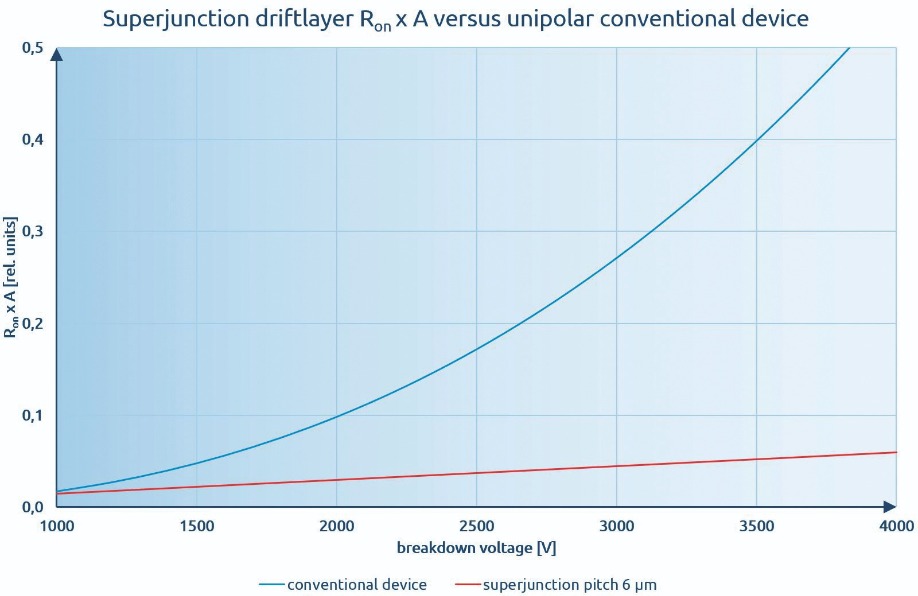
Figure 2. Drift layer on-resistance for conventional and super-junction SiC-power MOS, according to the theory described in Jpn. Patent 9701201.1
For silicon super-junction devices, manufacture tends to involve a multi-epitaxial approach. It begins by ion implanting p- and n- areas side-by-side in an undoped epitaxial layer to define the p-type pillars. Another epi layer is deposited on top, before the implanting process is repeated. Carrying out these steps up to five-to-ten times creates ohmic p- and n-pillars, which are then subjected to a high-temperature diffusion process (see Figure 3).
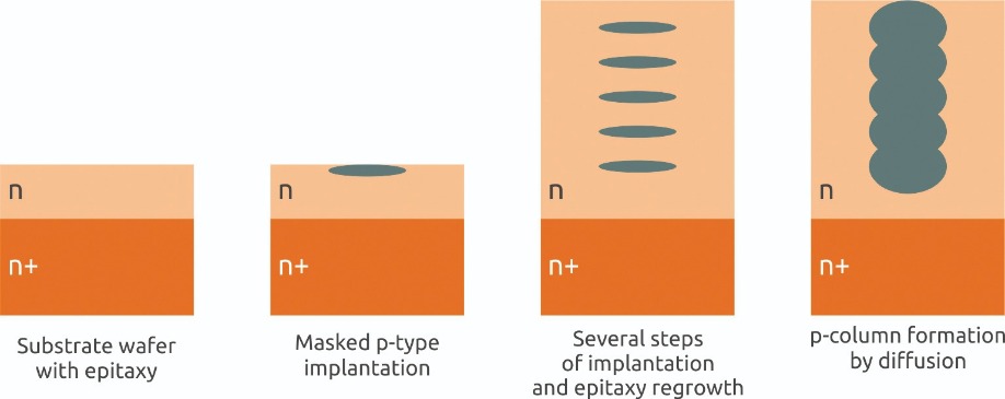
Figure 3. The manufacture of silicon super-junction devices includes a multi-epitaxy manufacturing step.
Whatever approach is used has to ensure charge-balancing in the device – and so must realise highly precise doping. That rules out technologies like p-doped epi trench filling, because the doping accuracy in the high-volume production of SiC epitaxial layers is rarely better than between +/- 10 percent and +/-20 percent.
The good news is that there is a solution that is applicable to high-volume production: ion implantation, but without diffusion. We are pioneering a form of this at mi2-factory in Jena, Germany. Our technology is capable of producing deep custom-tailored dopant profiles, and while its application to semiconductor manufacturing is new, in a slightly modified flavour it has been successfully applied in heavy-ion cancer therapy for many years.
Our approach differs from the conventional one, whereby monoenergetic ions are ‘shot’ into a pre-defined depth region known as the projected range. In that case, for a given substrate and ion combination, the projected range is just defined by the ion energy. A single shot creates a gaussian peak of implanted ions. However, it is possible to form extended profiles by creating a sequence of many gaussian profiles, each originating from a different implant energy (see Figure 4).
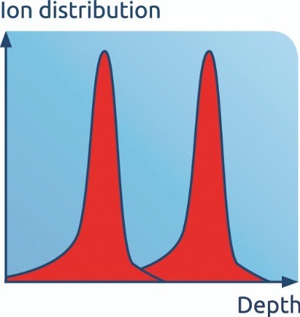
Figure 4.Two ion implantations with different energies result in essentially gaussian peaks.
We advocate a far simpler approach: one shot, one ion energy and a very special filter. Known as energy filter for ion implantation, our technique involves the use of a micropatterned membrane, which converts a monoenergetic ion beam into a continuum of ion implant energies (see Figure 5). With the membrane in the path, ions are ‘shot’ not only into one depth, but simultaneously into all depths, where maximum depth is defined by the primary ion energy. With this approach, continuous depth profiles are accomplished in a very straight forward manner (see Figure 6).
Armed with our technology, high-volume manufacture of SiC super-junction transistors is possible. Our approach eliminates the need for diffusion, replacing this with a technique that delivers an extremely high level of precision. Production costs are low – just one step is required for ion implanting, with a process that is capable of both aluminium p-type doping and nitrogen n-type doping.

Figure 5. The energy filter for ion implantation pioneered by mi2 factory. The energy of primary ions is modified according to the path length individual ions have to travel through the filter membrane. The long path – through peak – leads to a high loss of energy, while the short path – through a valley – leads to a low loss of energy.
Although the membranes for our energy filter for ion-implantation technology are consumables, that does not prevent them from supporting stable, reliable processing. Depending on the ion dose, as many as one hundred 6-inch wafers may be implanted with just a single membrane. Given the very low membrane cost per implant, chip costs generally fall when using our technology, due to benefits that include a reduction in device dimensions associated with the super-junction design.
While our ion-implantation technique may make its case most strongly for the super-junction transistor, it also has a role to play in improving the performance of other SiC power devices, via improvements in doping accuracy (see Figure 7).
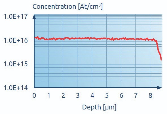
Figure 6. Nitrogen depth profile for 1200 V SiC devices.
This claim for a reduced chip size is supported by work that we carried out several years ago. Back in 2014, in collaboration with an industry partner, we took part in an R&D project to investigate the impact of doping precision. During this programme, we compared the variations in key characteristics of 600 V merged p-i-n Schottky diodes from regular production with those formed with our ion-implantation technology. We found far narrower parameter distributions for differential resistance, blocking voltage and leakage current, highlighting the potential of our energy filter for ion-implantation technology to reduce chip sizes (see Figure 8).

Figure 7. The energy filter for ion-implantation technology developed by mi2 factory can be used for making diodes and transistors.
Today, our technology is well-placed to provide the essentially homogenous doping profiles that are needed for diodes and super-junctions. In future, the design of these devices is tipped to evolve, with the introduction of graded drift-layer doping profiles that will propel efficiency to a new level. We intend to support this, having just started to develop an advanced form of our technology that will be capable of delivering more complex doping profiles.
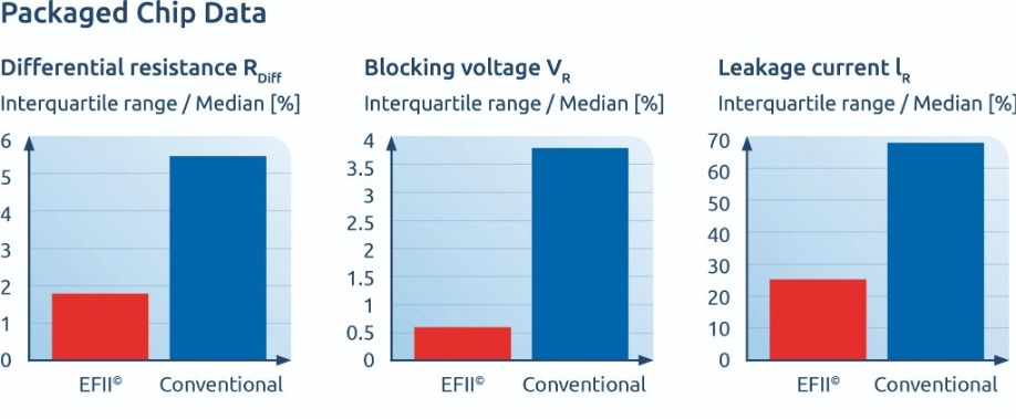
Figure 8. Results from an early R&D project with a chipmaking industrial partner highlight the reduction in the spread of key attributes for diodes.
We are confident that interest in our technology will grow. The SiC super-junction is destined to deliver a hike in power-transistor efficiency, and our energy filter for ion-implantation technology is a key enabling technology for the production of these devices. Other diodes and transistors will also benefit from our approach to doping, with the greater accuracy provided by our technology enabling a trimming of dimensions, leading to significant cost savings.
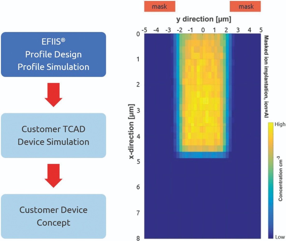
Figure 9. Left: The approach that mi2 factory takes for supporting customer device design with its energy filter for ion-implantation. Right: A 5 µm-deep p-column created in SiC using an energy filter for ion-implantation.
T. Fujihira et al., “Semiconductor device with alternating conductivity type layer and method of manufacturing the same,” Jpn. Patent 9701201.1 (1997)
G. Deboy et al. IEDM 683 (1998)
F.Udrea et al. IEEE Trans. Electron Devices 64 713 (2017)
R. Rupp et al. Materials Science Forum 858 531 (2016)
S. Agostinelli et al. Nucl. Instrum. Methods Phys. Res 506 250 (2003)
PC-based control and EtherCAT technology from Beckhoff aids Agnitron’s modular design of MOCVD tools, which can be used for the growth of gallium oxide and III-nitride epilayers
BY ANDREI OSINSKY, DMITRY VOLOVIK AND IVAN YUNCHYK FROM AGNITRON
Gallium oxide (Ga2O3) has tremendous potential. This ultra-wide bandgap material promises to enable a new generation of more efficient, better designed high-voltage switches that can serve in consumer electronics, and also in defence technologies deployed on ships and aircraft.
Before this happens, it is necessary to prove the capability of Ga2O3 and its related devices. To do this, large-scale efforts are underway, such as those run by the US Air Force Office of Scientific Research, and the Multidisciplinary Research Program within the University Research Initiative, which is sponsored by the US Department of Defence. Through these initiatives, researchers in the US are gaining greater insight into how to dope Ga2O3, and the nature of the imperfections in this material.
These programmes involve scientists and engineers at various academic institutions, including Ohio State University, the University of California Santa Barbara, Cornell University, Georgia Institute of Technology, Washington State University and the University of Utah. For all these academic teams, one of the biggest challenges is finding MOCVD tools that can meet the customisation, price and reliability requirements to handle Ga2O3 properly.
When Sriram Krishnamoorthy from the University of Utah faced this challenge, he started to investigate the capability of new systems. This search led him to discover the highly versatile Agilis platform produced by our team at Agnitron of Chanhassen, MN. Our company directs efforts at expanding MOCVD machine modularity, so that this can better serve end users in research and development and at small-to-medium-size production facilities. However, that is by no means all that we do: we also refurbish legacy systems; we have launched an in-sit metrology tool, Agnitemp; and we conduct our own research in ß-Ga2O3 applications.
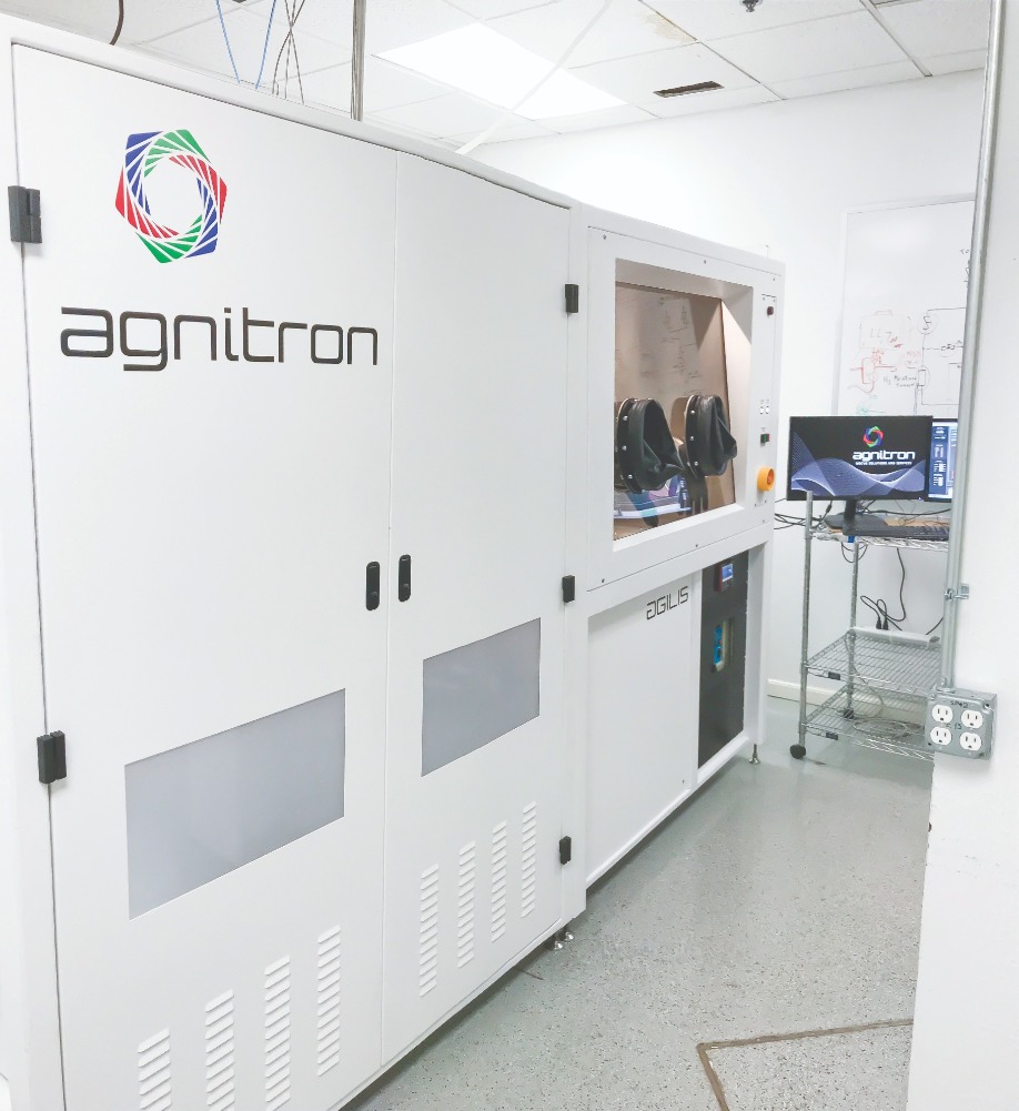
The Agilis machine line from Agnitron provides the optimal MOCVD platform for research and development, as well as smaller production facilities.
This capability, not a feature on MOCVD machines by other manufacturers, provides incredible value for researchers. If clients require funding for research and development, they can now pursue grants and funding opportunities on more than one material system as a result of the dual use system, increasing their odds of success.
Customising the system
Our experience in refurbishing legacy systems has aided our efforts in the design and construction of a dual-use MOCVD platform. For both tasks, cost and reliability are key priorities, so our design process begins and ends with modularity. From software to individual components, the machines must easily adapt to unique customer requirements, whether that means additional human-machine-interface features, increased input/output count or enhanced processing power. The growth tool must communicate in real-time with existing systems in a lab or production facility. The MOCVD reactors that we offer include developmental reactor design, and showerhead configurations combining high-quality material with rapid growth rates. Supporting our customers as they refine their MOCVD processes plays an essential role in the scaling of their technology, so that it delivers commercial success.
Cost is a major factor when purchasing an MOCVD system, as the price of these tools can easily surpass $1 million. Even equipped with the dual-use capability of the Agilis, this is a significant capital investment for our customers, who typically do not possess the kinds of budgets that giant semiconductor manufacturers do.
Our customers have ever-increasing data acquisition requirements, whether they are undertaking research, or producing epiwafers that must meet high-quality standards and adhere to growth recipes. So it is crucial to add functionality and processing power while avoiding a hike in cost, a dramatic change in system design and any compromise to reliability.
Within the compound semiconductor industry, reliability means that new components retain the deposition recipes of legacy systems, while providing greater dependability. These attributes are invaluable, given that a customer may have devoted years of development work and millions of dollars to define processes. They want a new system that can be programmed to maintain the semiconductor recipe exactly, with no unplanned downtime.
We have strived hard to provide this level of service. It’s not easy – there was a time when we encountered reliability issues associated with a previous vendor’s automation and control systems. Those issues were so serious that we were on the verge of losing customers. But that is now completely resolved, thanks to our switch to a new supplier, Beckhoff Automation.

For production intensive applications, Agnitron implements the many-core CX2042 Embedded PC from Beckhoff, which boasts a quad-core, 2.2 GHz Intel Xeon processor with four cores, with a 1 terabyte solid-state drive.
When we were under tremendous pressure to find a reliable, open solution, our experts visited the US headquarters of Beckhoff in nearby Savage, MN. In Beckhoff, we found a partner with a shared philosophy, with regard to innovation through flexible technologies. We were delighted to work with them, and assured by their free technical support to our engineers, both over the phone and in person. Initially, this set our mind at rest. Now, however, it is hardly ever required, because our engineers have grown so familiar with Beckhoff hardware and software.
Many machines within the compound semiconductor industry still use separate programmable logic controllers and PCs. In our view, though, it is far better to use PC-based controllers, an approach that gives us the edge over our peers.
With modularity in mind, we offer two different variants for the Agilis system: the Beckhoff CX2042 Embedded PC with a quad-core, 2.2 GHz Intel Xeon processor; and the Beckhoff CX2040 Embedded PC with a quad-core, 2.1 GHz Intel Core i7 processor. The CX2040 configuration meets the needs of research and development customers, and the CX2042-based hardware is better suited to production. That’s because our growing clientele in the production market require higher RAM and processing speed. The CX2042, which features a Xeon processor and a 1 terabyte solid-state drive, delivers this, providing the optimal controller for round-the-clock production environments. It allows the Imperium software and SQL database to run on the same hardware, thereby supporting more complex operations, with greater data collection, plus the metrology requirements of Agnitemp.
Preserving the recipe
Our Imperium control software takes full advantage of TwinCAT 3 automation software from Beckhoff and the real-time Windows kernel. The TwinCAT real-time kernel executes the time-critical diagnostic, safety and process control tasks, with each task assigned to different cores of a multi-core Intel Xeon processor. These tasks continue to execute even if the Imperium software is closed by the user or interrupted for any reason. Mirroring a typical hardware programmable logic control system, the Imperium process control recipes and execution of routines run outside the Imperium software itself, and are controlled by the TwinCAT real-time kernel. By fully utilising the speed, reliability, virtualisation and multi-core capabilities of the modern Intel processors, the system operates at unprecedented real-time task cycle times and delivers an exceptional level of performance. For example, Imperium production recipes have repeatably performed steps as short as 10 ms in length.
The Imperium-MOCVD software from Agnitron was built with TwinCAT 3 automation software from Beckhoff, and relies on the ability to program the machine logic in C# using Microsoft Visual Studio.
Our engineers, using TwinCAT 3 automation software as the engineering environment and runtime on the Embedded PCs, can write machine control logic in C# using Microsoft Visual Studio while accessing the TwinCAT runtime and input/output system. As a Windows-based device, the Embedded PC also allows them to install the Imperium control software and save data locally. This facilitates machine customisation without developing entirely new code. Note that Imperium was designed with a configurable concept, so that engineers can reconfigure a control software package for a tool through a series of menus without the need to reprogram anything. This capability stems from the modularity of Beckhoff products.
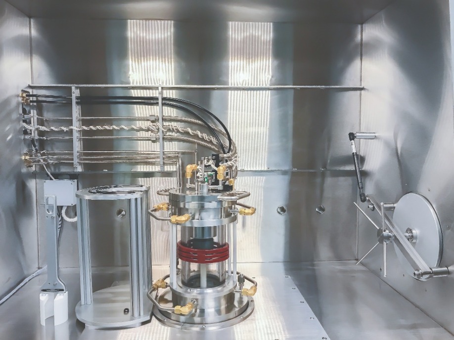
The Agilis platform offers a turnkey solution for R&D labs and small to medium-size production facilities. Agnitron also provides retrofit and refurbishment services as it has done since the company was founded in 2008.
The real-time networking capability of EtherCAT industrial Ethernet technology provides further benefits for the Agilis platform. High-density EL3318 EtherCAT Terminals connect Agilis to eight different thermocouples per terminal. This is a major benefit when working with ß-Ga2O3 and other complex semiconductor materials, as it is a challenge to optimise the temperature profile in the growth chamber.
A small footprint is possible with the high-density EL3318 EtherCAT Terminals, which can be used alongside 16-channel input/output terminals. That’s a major asset, as space is incredibly tight inside control cabinets, especially on smaller R&D systems.
As with TwinCAT 3, using EtherCAT makes it easier to commission units and customise them in the field. Highly valued is its flexibility to connect with legacy DeviceNet equipment: EtherCAT is now the leading semiconductor industry network, and a SEMI standard of today, overtaking DeviceNet, the previously accepted industry-wide standard. The EL6752 DeviceNet Master/Slave Terminal creates a bridge between the Beckhoff controller, the EtherCAT network and DeviceNet field devices in customer facilities.
Using auto configuration capabilities, our engineers can easily connect new and legacy devices over EtherCAT without data loss. For example, it takes them just a few hours to integrate a DeviceNet network using EtherCAT and the TwinCAT development environment. In comparison, this could take a week using technology from a previous vendor.
Our strategic choice of automation and control technology enables us to produce competitively priced modular systems with increased reliability. The Agilis platform also produces films with great attributes. According to Krishnamoorthy, epilayers grown with this tool have the highest mobility and aluminium incorporation, alongside a ground-breaking low-background concentration that is critical for low-doped drift layers for high-voltage power electronics.
What’s more, the strengths of the dual-use chamber could extend beyond simply studying either ß-Ga2O3 or III-nitrides. For example, Krishnamoorthy has submitted proposals to explore III-nitride and Ga2O3 integration for very high-voltage vertical device applications. The Agilis platform is a very affordable option for pursuing that type of research.
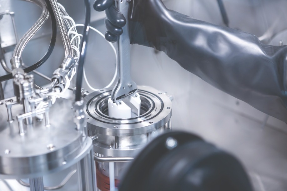
The Agilis MOCVD system further enables research into gallium oxide and its potential for electronics. In addition, a new dual-use machine provides the unprecedented ability to work with multiple materials with minimal changeover times.
The benefits associated with Beckhoff technology also transform our refurbishment and retrofit projects, which can include the installation of the CX2040. We don’t always take that approach, however – if existing programmable logic controllers are in acceptable working condition, we simply replace legacy PCs with a Beckhoff C5102 rack-mounted Industrial PC (IPC). Whichever route is taken, backward-compatibility of Beckhoff hardware and software ensures that semiconductor growth recipes are reliably maintained. In contrast, when we worked with other vendors, it was not uncommon to plug a decades-old PCI card into a new PC and be faced with a formidable blue screen.
By drawing on the wide and growing range of products in the Beckhoff portfolio, we have the capability to quickly adapt to customer specifications. According to Beckhoff, this is the norm: it finds that its open system architecture aligns well with its customers’ unique requirements.
Following ten years of successful innovation, our plan is to continue to create powerful, modular solutions that break new ground for semiconductor research and production. These efforts will continue to involve our collaboration with Beckhoff, which is an outstanding partner for automation and control. As the company continues to innovate, we look forward to incorporating its new technologies in our products, as this will enable us to further customise and enhance our MOCVD systems.
The authors are grateful for the support and expertise provided by: University of Utah Assistant Professor of Electrical and Computer Engineering Sriram Krishnamoorthy, Agnitron Equipment Engineer Nazar Orishchin and Beckhoff Automation Marketing Communications Specialist James Figy, who also contributed research for this article.
Gallium oxide Schottky barrier diodes incorporating narrow trenches are setting new benchmarks for voltage blocking and leakage current
BY WENSHEN LI, ZONGYANG HU, KAZUKI NOMOTO, DEBDEEP JENA AND HUILI GRACE XING FROM CORNELL UNIVERSITYIt’s of little surprise that there has been a consistent drive toward the use of wider bandgap materials for power electronics. After all, the wider the bandgap, the greater the breakdown field, opening the door to making devices with a higher breakdown voltage for the same material thickness.
However, nature is not always that generous. Typically, a move to a wider bandgap is accompanied by more challenging doping, along with difficulty in making high-quality native substrates. Judged in these terms, gallium oxide appears to offer a sweet spot beyond SiC and GaN.
One of the most promising forms of gallium oxide is its b-phase, which has a bandgap of 4.5-4.7 eV. Luckily, it is easy to dope this oxide n-type in a controllable manner, to realise doping that spans 1015 cm-3 to 1020 cm-3. Thanks to shallow donor levels throughout this range, doping efficiency is high at room temperature. Another encouraging aspect of Ga2O3 is that single-crystal substrates of this material can be readily produced with melt-growth techniques, mirroring the manufacture of those made from silicon. Given all this promise, is it possible to harvest all the benefits arising from the large bandgap of Ga2O3 and demonstrate devices that are superior to those made from SiC and GaN?
To help answer this question, our team at Cornell University has been focusing on the development of Ga2O3 vertical power devices. By employing a vertical topology, they are capable of carrying more current per chip area, while taking advantage of the readily available Ga2O3 single-crystal substrates. Our goal is to demonstrate the highest unipolar performance that Ga2O3 can deliver – it is projected to be far higher than that of SiC and GaN, primarily due to a leap in the breakdown field to 6-8 MV/cm, arising from the superior bandgap.
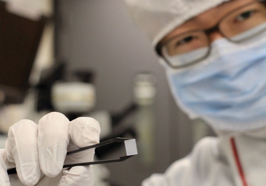
A judicious junction
A drawback of Ga2O3 is its lack of p-type doping.
Due to this drawback, we incorporate metal-insulator-semiconductor (MIS) junctions in our devices to enhance their blocking voltages. As we’re about to see, the reason behind using of this form of junction is far from trivial.
Let us begin by considering a MIS structure under reverse bias: the semiconductor enters deep depletion near the junction, and a so-called inversion layer results, due to thermal energy within the device promoting electrons from the valence band to the conduction band. This is not good news, as once the inversion layer is created, the entire reverse bias is dropped across the insulator of the MIS structure, leading to catastrophic failure of the insulator and thus the power device. The only option for preventing this catastrophe from taking place is to evacuate the resulting minority carriers quickly. In our case, that means evacuating the holes in an n-type semiconductor.
A key figure-of-merit in this process is the time constant associated with the inversion process (as can be seen in Figure 1, this characteristic is governed by the bandgap).
For semiconductors with a small-bandgap, such as silicon and GaAs, at room temperature an inversion layer forms within seconds or minutes; and at elevated temperatures, where a power device often operates, this time is far shorter, as the time constant plummets by several orders of magnitude. So, in silicon and GaAs devices, a proper p-type contact is needed to sweep out the holes that are generated by either thermal generation or impact ionization.
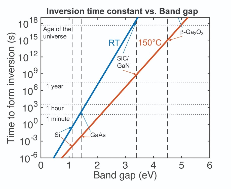
Figure 1. The estimated inversion time constant in MIS-junctions as a function of the bandgap. The time to form the inversion layer increases exponentially with increasing bandgap, allowing for the use of a MIS-junction for voltage blocking in wide bandgap semiconductors without the concern for MIS-junction snapback with time. Or, to view this graph from another perspective, there is a necessity to employ p-type contacts in narrow bandgap semiconductors, but they can be avoided in wide bandgap semiconductors.
In fact, for Ga2O3, the electric field required for impact ionisation is so high that it can hardly be supported by a true insulator. Even if impact ionisation happens, the generated holes are highly localized, due to the polaron effect and the super flat valence band. This makes it very difficult to evacuate these holes, and the best way forward is to suppress their formation in the first place.
Based on the arguments that we have just presented, we are pursuing an architecture that employs a MIS-junction for voltage blocking and avoids a p-n junction. The significance of the time constant associated with inversion layer formation in a MIS structure is not widely known. However, it is another important virtue of wide bandgap and ultra-wide bandgap semiconductors.
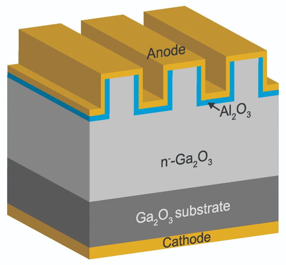
Figure 2. The Ga2O3 trench-MIS Schottky barrier diode features a periodic fin channel, formed by etched trenches. MIS-junctions covering the trenches provide a charge-coupling mechanism that effectively reduces the electric field near the top Schottky contact.
We have focused our efforts on the development of a Schottky barrier diode. This device is capable of a fast switching speed, due to unipolar operation, but it is compromised by a lower breakdown voltage and a higher leakage current. To address both of these drawbacks, we engineer a charge-coupling mechanism around the Schottky contact. The result: a trench-MIS barrier Schottky diode (see Figure 2), a device that effectively reduces the electric field near the top Schottky contact.
Simulations of a form of our devices, which has a fin channel width of 1 µm and a trench depth of 1.5 µm, reveal the electric field profile when the diode is blocking 2.44 kV – this is the highest breakdown voltage we have achieved so far. According to these calculations, the charge-coupling mechanism reduces the electric field near the Schottky contact to below 1 MV/cm. Due to the trench structure, termination of the electric field is predominantly to the metal at the sidewall, rather than to the top Schottky metal. In contrast, in a regular Schottky barrier diode that does not gain the benefit of the charge-coupling effect, the surface electric field is 4 MV/cm. This value is so high that it leads to an unacceptably-high leakage current density.
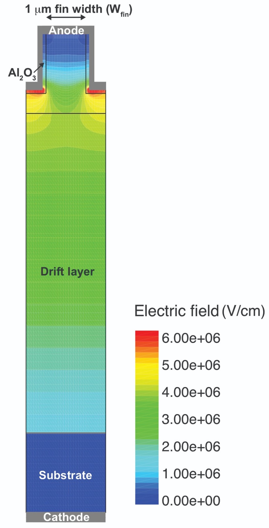
Figure 3. The simulated electric field profile in a unit cell of a trench diode with a fin channel width of 1 µm at 2.44 kV. Even though the highest parallel-plane electric field reaches 4.3 MV/cm, the electric field near the Schottky contact is less than 1 MV/cm, thanks to the charge-coupling effect provided by the trench-MIS structure. The field peaks at 5.9 MV/cm near the bottom of the trenches.
We produce our diodes on (001) oriented epitaxial wafers. They are produced by Novel Crystal Technology using HVPE. The drift layer, which has a net doping concentration of around 2×1016 cm-3 and a thickness of 10 µm, is designed for making devices capable of blocking 3 kV.
To investigate the influence of the fin geometry, we have produced our portfolio of diodes with fin channel widths ranging from 1 µm to 8 µm. The narrower the fin, the greater the reduction in the surface electric field, and thus the lower the expected leakage current density.
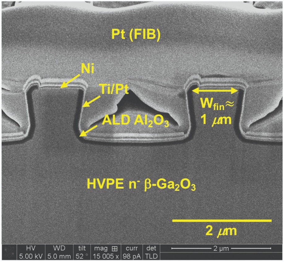
Figure 4. A scanning electron microscopy, cross-sectional image of the trench Schottky barrier diode reveals a smoothly curved trench corner profile, which is beneficial for mitigating the field crowding effect.
Trimming leakage, boosting voltage
As expected, our trench Schottky barrier diodes turn-on at 1.25 V, a figure similar to that for a regular diode (see Figure 5). We find that the differential on-resistance of the trench diodes is governed by the ratio of the fin area to the total device area. When this figure is 50 percent, the trench Schottky barrier diode has a specific on-resistance of 10 mΩ cm2. In comparison, in a regular Schottky barrier diode this figure is just 7 mΩ cm2. The higher figure, stemming from the restricted current path within the fin channels, is the price to pay for the superior reverse blocking capability, which we will come to later on. Note that the increase in on-resistance is not fixed, and may be minimized by upping the fin area ratio and increasing the effective electron mobility in the fin channel.
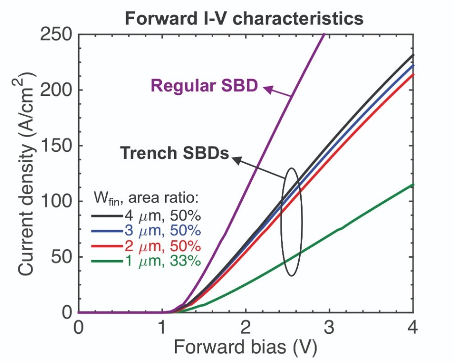
Figure 5. Forward current-voltage characteristics of the trench Schottky barrier diodes in comparison with a regular Schottky barrier diode. The turn-on voltage of all diodes is nearly identical.
Our fabrication process is yet to be optimised, and there is a certain degree of non-uniformity in the leakage current. In several 1 µm and 2 µm channel devices where the parasitic leakage current is minimal, the leakage current is below our measurement noise floor of 1 µA/cm2, even at voltages exceeding 2 kV. Such a low leakage is highly beneficial, because it translates into a trimming of off-state power loss.
Even when operating at 2 kV, our low leakage devices can have a power loss on the order of mW/cm2. This is very low – to put this figure in perspective, the reverse blocking voltage in commercial kV-class Schottky-based devices is typically specified at a leakage current density of around 1 mA/cm2.
It is possible the commercial devices could sustain even higher voltages than the specified blocking voltage without destructive breakdown. However, operating in this regime would increase their leakage current and induce a high off-state power loss. In other words, the full voltage-blocking capability of the material may not be fully utilized due to the constraint imposed by the leakage current. By cutting the leakage current, we will be able to probe the intrinsic voltage handling capability of the material. Understanding the fundamental limit of Ga2O3 is essential in our push toward understanding the practicality of devices made from ultra-wide bandgap materials.
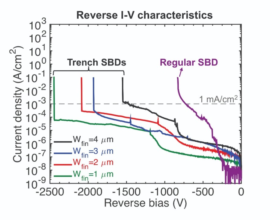
Figure 6. Reverse current-voltage characteristics of the trench Schottky barrier diodes in comparison with a regular Schottky barrier diode. The trench diodes possess a lower leakage current density as well as higher breakdown voltages.
To understand this trend, we have simulated the electric field profile at reverse bias for all our fin widths. These calculations reveal that due to field crowding, the electric field peaks at the trench bottom corners within the device’s active region. In narrower channels, the field peak is smaller, due to a reduction in space charge. Higher field peaks are best avoided, as they impair the breakdown voltage.
According to our simulations, for all widths of fin, the peak electric field in Ga2O3 hits 5.9 MV/cm at the diode’s breakdown voltage. This suggests that all our diodes, regardless of their fin width, break down at the trench corners. So, to realise high blocking voltages, smooth corners must be used alongside narrow fins. However, note that even with our latest un-optimised design, the highest parallel-plane electric field is 4.3 MV/cm, a value unreachable in SiC and GaN.
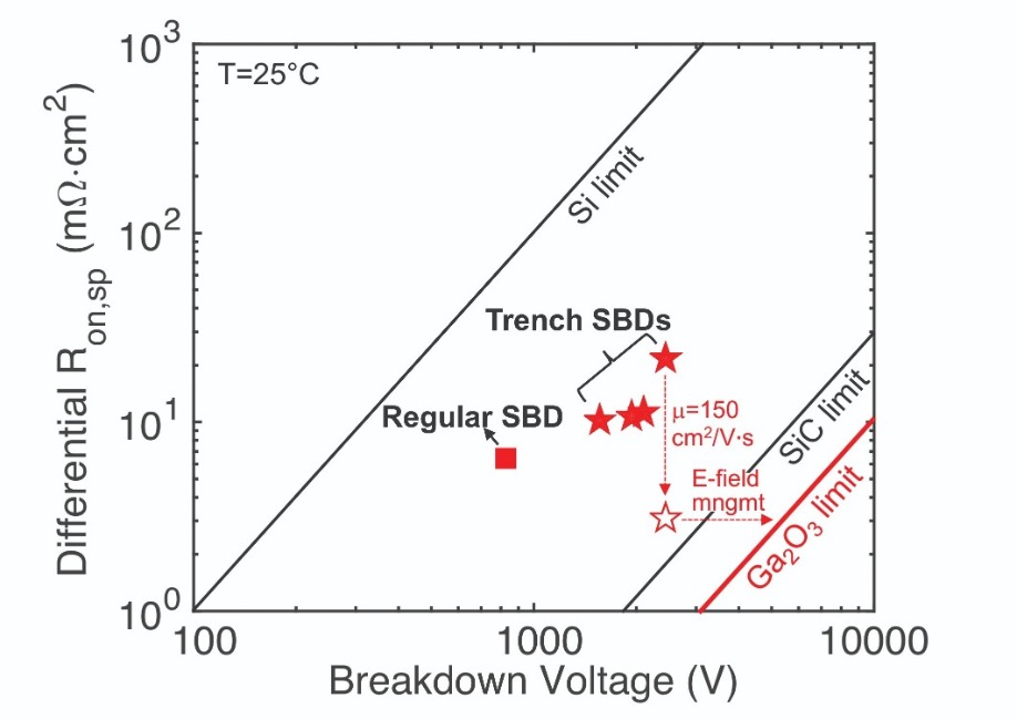
Figure 7. Trench Schottky barrier diodes fabricated at Cornell University deliver state-of-the-art performance for a vertical Ga2O3 power device. An increase in electron mobility, alongside improvements to electric field management, could spur performance to close to that of the Ga2O3 limit.
A parallel effort of ours is the development of vertical fin channel transistors. Using a similar architecture to that of our diodes, we have fabricated the first normally-off transistor with a breakdown voltage higher than 1 kV. This result, reported last year, came from a transistor with a figure-of-merit exceeding the silicon unipolar limit.
Since then, we have increased the breakdown voltage of our normally-off transistors to more than 1.6 kV, while maintaining excellent on-resistance. As our vertical fin channel transistor shares many similarities with our trench Schottky barrier diodes, the insights that we have obtained to the device physics of these trench diodes, and also the process optimisation for this device, can be directly applied to our transistor efforts.
Marching on
At last December’s International Electron Devices Meeting (IEDM), we reported results for our trench diodes, showing that these devices set new benchmarks for breakdown voltage and the Baliga’s figure-of-merit in vertical Ga2O3 power devices. Pulsed measurements on our diodes with a 2 µm fin channel produce a Baliga’s figure-of-merit of 0.45 GW/cm2. These devices surpass the silicon unipolar limit (Figure 8), but are yet to reach the SiC limit.
Analysing the on-resistance indicates that in our latest diodes, the effective mobility is much lower than expected. We attribute this to either un-optimised surface treatments or the starting wafer quality.
If we were able to realise a mobility of 150 cm2 V-1 s-1, which has been reported in lightly-doped Ga2O3 (~1015-1016 cm-3), the on-resistance of our trench diodes would fall by a factor of three to just 3 mW cm2, leading to a projected figure-of-merit very close to the unipolar limit for SiC. Such a mobility is not pipe dream, given that the measurements for the highest room-temperature mobility in ß-Ga2O3 are around 180 cm2 V-1 s-1.
Today sales of SiC are rocketing, with GaN not far behind. This demonstrates that wide bandgap devices are starting to fulfil their promise. Next on that list will be Ga2O3, which is now making rapid progress. While the lack of native p-type doping is hampering the adoption of some conventional designs, by turning to building blocks such as MIS-junctions, we have shown that functional power devices can be made that deliver good performance. It is clear that backed up by melt-grown high-quality native substrates, Ga2O3 is able to deliver power devices with unprecedented unipolar performance and mass-production capabilities.
W. Li et al. in IEDM Tech. Digest 2018 p. 8.5.1
W. Li et al. Appl. Phys. Lett. 113 202101 (2018)
Z. Hu et al. IEEE Electron Device Lett. 39 869 (2018)
The three major weaknesses of GaN LEDs – the efficiency droop, the green gap, and the electrical potential drop – all result from changes to the recombination coefficients, which vary with carrier density
BY DONG-PYO HAN, SATOSHI KAMIYAMA, TETSUYA TAKEUCHI, MOTOAKI IWAYA AND ISAMU AKASAKI FROM MEIJO UNIVERSITY AND NAGOYA UNIVERSITY, JAPAN
What is the perfect source of light? Surely, it is one that waste no energy in producing photons that span the deepest violets to the near infra-red, much like the visible rays from the sun. Judged in these terms, the emission from solid-state sources that combine the output of red, green and blue LEDs is encouraging. However, there is still much room for improvement.
Consider the blue and green sources, made from nitride-based LEDs that feature GaInN quantum wells. For these devices, performance is pegged back by three phenomena: droop, the gradual decrease in efficiency as the drive current increases; the green gap, the gradual decrease in efficiency as the indium content in the multiple-quantum-wells rises, to push emission to longer wavelengths; and the electrical potential drop, which leads to dramatic increases in the voltage that must be applied to provide an increase in the driving current.
Addressing all three of these would lead to a dramatic improvement in the quality of the LED light source. It would allow it to operate at a higher efficiency, while delivering a strong spectral output across the entire visible spectrum.
Much effort has already been devoted to uncovering the physical mechanisms responsible for the efficiency droop and the green gap. Researchers have considered carrier overflow/spill-over, carrier localization/delocalization, piezo electric fields, and asymmetric carrier distributions in multiple quantum wells, and tunnelling leakage currents. Many of these investigations have concluded that an increase in a non-radiative recombination process is to blame for the declines in efficiency with higher current densities and longer wavelengths.
Meanwhile, the numerous studies on the electrical potential drop have tended to focus on either current crowding caused by a lateral structure, an insufficient contact potential barrier between the metal and the semiconductor, a high magnesium-acceptor activation energy, or a heavy effective mass for the hole. Often, the problem has been thought to be due to the ohmic potential drop.
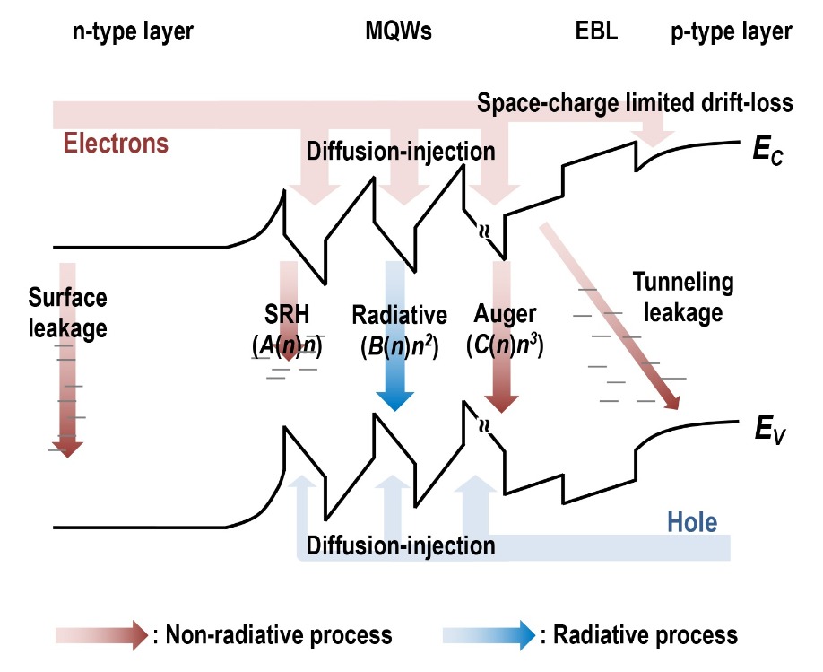
Figure 1. Overall carrier transport/recombination process in the operation of the GaInN-based LED.
It is well-established that a lower value for the internal quantum efficiency occurs when fewer electrons that are injected into the quantum well are converted into photons. When the internal quantum efficiency falls, this can account for the green gap and the efficiency droop – and it can also be an indirect cause for the electrical potential drop. So, it is clearly important to understand the internal quantum efficiency of the LED, as this can aid the development of artificial white-light sources that take efficiency to a new level.
We have developed an accurate understanding of the internal quantum efficiency of the LED by beginning with an examination of the carrier transport and recombination processes inside the device, using an energy-band diagram (see Figure 1). There are essentially three parts to carrier transport: diffusion-injection from n- and p-bulk layers into the multi-quantum well active region; space-charge limited drift-loss to the opposite bulk layer, due to carrier overflow or spill-over; and leakage currents, arising through the surface defect and the tunnelling leakage current through threading dislocations.
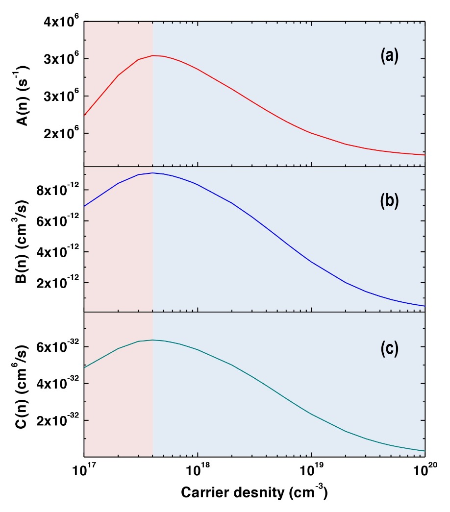
Figure 2. Numerical calculation results of (a) A(n), (b) B(n), and (c) C(n) coefficients as a function of carrier density n, respectively.
To arrive at a deep understanding of the internal quantum efficiency, it is essential to examine the coefficient of each recombination process. As shown in Figure 1, the carriers that are inserted into the multiple quantum wells from the n-type and p-type layers lose their energy through each recombination process. In general, up until now, simply A, B, and C coefficients have been used to express the various processes in the form of the terms, An, Bn2, and Cn3, that are united in what is known in the LED research community as the ABC model. Within this framework, the A, B, and C coefficients are considered to be fixed in value, and independent of the carrier density.
Varying coefficients
However, our research reveals that this approach is fundamentally flawed. That’s because the ABC coefficients are not fixed, but have great dependency on the drive current and the carrier density (see Figure 2). For all three coefficients, values rise with carrier density, before peaking and then declining substantially.
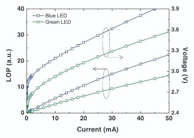
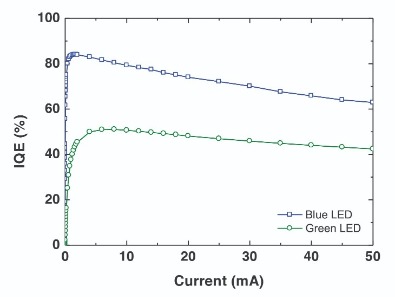
Figure 3. Measurements of (a) the light output power and applied voltage as a function of driving current and (b) the internal quantum efficiencies (IQEs) as a function of driving current for the blue LED and green LED, respectively.
To gain a greater insight into the two efficiency degrading issues, it is critical to be able to measure the internal quantum efficiency of the LED as a function of drive current. Recently, we have developed a highly reliable way to do this, deriving a value from dependency of the general ABC coefficients.
Our approach is to determine the absolute value for the internal quantum efficiency from one of the properties of the ABC coefficients – that they have inflection points at the same carrier density. We also draw on the mathematical model, making use that the differential of the radiative current and non-radiative current is constant only at the driving current where ABC coefficients have inflection points.
Using this approach, our measurements on blue and green LEDs that were made by our collaborators at Meijo University have enabled us to produce plots of light-output-power as a function of driving current and applied voltage (see Figure 3 (a)). As expected, the light-output-power of the green LED is generally lower than that of the blue LED. Also note that at high currents, the electrical potential drop – that is, the slope of the current-voltage curve – is higher for the blue LED than its green cousin.
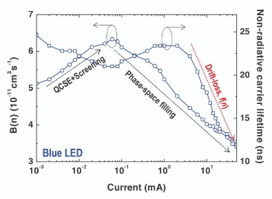
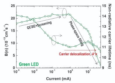
Figure 4. Measurement results of B(n) and non-radiative carrier lifetime as a function of driving current for the (a) blue LED and (b) green LED, respectively.
To examine the three efficiency degrading issues in more detail, we have delved deeper into the LED’s carrier recombination and transport dynamics. While doing so, we have made sure that we have investigated the recombination coefficients as a function of current for each sample.
Recently, we reported that one way to determine the recombination coefficient as a function of drive current is to combine the results of the how the: differential carrier lifetime, which is determined from impedance measurements, varies with drive current; with the result of plots of the internal quantum efficiency for different currents. Using this method, we have measured the recombination coefficients as a function of current for blue and green LEDs (see Figure 4(a) and (b)).
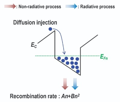
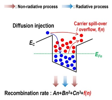
Figure 5. Carrier dynamics inside the multiple quantum well (MQW) of a blue LED: (a) at low current density; (b) at high current density.
Comparing blues and greens
Comparing the blue and green devices reveals that the value of B for the green LED is about ten times smaller than that of its blue sibling, and its degree of decrease at high current is more severe. However, for the blue LED this coefficient decreases rapidly in the non-radiative carrier lifetime high-current region, while the green emitter does not exhibit such a drastic change. Note that for both the blue and green LEDs, the absolute value of non-radiative carrier lifetime at high-current region are similar to each other. That is, the non-radiative process is not the primary cause of the green gap.
Armed with these insights, we have searched for the reason behind the similarities and the differences in the carrier recombination and transport characteristics of the green and blue LEDs. We were also keen to discover how these characteristics would impact LED performance, and what their relationship is with the aforementioned three efficiency degrading phenomena.
Our efforts have given us a new insight into the behaviour of both blue and green LEDs. For blue LEDs, when driven at a low current, the carrier recombination rate is considerably larger than the carrier injection rate. In this regime, every injected carrier recombines, losing its energy inside the multi-quantum well, which has a carrier density determined by the quasi-Fermi level (see Figure 5(a)).
As the current is cranked up, the ABC coefficients gradually decrease, and the increase in the recombination rate fails to keep pace with the increase in the injection rate. Consequently, there comes a time when the carrier injection rate exceeds that of the carrier recombination rate.
At this point, carriers start to gradually accumulate inside the multi-quantum well. In some cases, they even show the same characteristics as those of the hot carrier. If they do, they acquire enough energy to overcome the barrier and escape from the wells to the opposite layer. This spill-over, or overflow, results in efficiency droop (see Figure 5(b)). For the hot carriers that accumulate inside the wells, the result is a space-charge, with current flowing in the form of a space-charge limited drift-leakage current that causes the electrical potential drop (see Figure 1 and Figure 3(a)). So, the efficiency droop and the electrical potential drop are interconnected phenomena in blue LEDs, both caused by a decrease in the recombination coefficient.
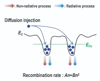
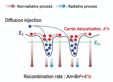
Figure 6. Carrier dynamics inside the multiple quantum well (MQW) of a green LED: (a) at low current density; (b) at high current density.
Like the blue LED, the ABC coefficients of the green LED decrease gradually with increases in current. Due to this, there is a point at which the carrier injection rate of the green LED exceeds the carrier recombination rate, and the accumulated carriers exit from the localization centre. However, the key difference with green LEDs is that the carriers that exit the localization centre lose their energy in additional Shockley-Read-Hall recombination when inside the wells, due to the high density of non-radiative recombination centres inside this active region.
Judged in terms of the non-radiative carrier lifetime, there is just a small difference between the blue LED and the green LED (see Figure 4). But the value for the B coefficient, which is a function of the carrier density, is about ten times smaller for the green LED than itsblue cousin. This implies that the difference in internal quantum efficiency (see Figure 3) – that is the green gap – is mainly determined by the difference in the B coefficient.
Why should the B coefficient vary so much between the blue and green LEDs? It is due to the complex interaction between: the quantum-confined Stark effect, which is caused by the relatively strong piezo electric field; and the decrease in the density of state of active region, resulting from the potential fluctuation followed by the decrease in the quantization dimension for the green LED. The quantum-confined Stark effect drives apart the hole and electron wave-functions in real-space, while the localization results in the separation of the hole and the electron wave-functions in k-space. The upshot is a dramatic fall in the carrier-density-dependant B coefficient, which accounts for the green gap.
Our work shows that efficiency droop is caused by the decrease of the ABC coefficient, triggering space-charge limited drift-loss that makes an electrical potential drop, while the green gap is caused by the decrease of B itself. While the non-radiative processes caused by them are different, the cause of both these phenomena is the same: the degradation of the B coefficient.
We have studied the three biggest impediments to high-efficiency LEDs: the efficiency droop, the green gap, and the electrical potential drop. Our work breaks new ground by examining all three of these maladies from the viewpoint of the reduction of recombination inside the multi-quantum well. All three impediments are, in principle, identical. Therefore, they can be simultaneously addressed by improving the radiative recombination among the recombination processes within the wells.
The authors would like to thank Prof. Dong-Soo Shin and Prof. Jong-In Shim at Hanyang University, Korea, for the valuable discussion and motivation. This work was supported by MEXT Private University Research Branding Project, MEXT Program for research and development of next-generation semiconductor to realize an energy-saving society, JSPS KAKENHI for Scientific Research A [No.15H02019], JSPS KAKENHI for Scientific Research A [No.17H01055], JSPS KAKENHI for Innovative Areas [No.16H06416] and Japan Science and Technology CREST [No.16815710].
D.-P. Han et al. Phys. Status Solidi A 210 2204 (2013)
D.-P. Han et al. Appl. Phys. Lett. 105 191114 (2014)
D.-P. Han et al. Appl. Phys. Express 9 081002 (2016)
D.-P. Han et al. Appl. Phys. Express 10 052101 (2017)
D.-P. Han et al. Appl. Phys. Express 10 122101 (2017)
D.-P. Han et al. IEEE J. Quantum Electron. 54 3200107 (2018)
D.-P. Han et al. Appl. Phys. Express 12 032006 (2019)

Multi-layer graphene quashes defects in AlN, leading to a hike in LED efficiency
Researchers from Beijing have cranked up the output power of deep UV LEDs by inserting a layer of graphene between the substrate and the epilayers.
The team’s efforts could aid the development of more powerful deep UV sources for the likes of sterilisation, polymer curing, biochemical detection and speciality lighting. Today, the use of LED in these applications is held back by a low internal quantum efficiency – it is typically below 10 percent.
Improvements in the efficiency and brightness of the UV LEDs produced by the team from Beijing resulted from the first growth of high-quality AlN films on nano-patterned sapphire substrates by graphene-assisted quasi van de Waals epitaxy.
Using this approach, coalesce occured in films of AlN as thin as just 1 µm. This is one-third of the thickness for the standard method, involving the growth of AlN films on patterned sapphire. Substantial savings result, both in terms of growth time and material costs.
To understand the benefits of their approach, the team undertook first-principles calculations to determine energy migration barriers for aluminium on sapphire and on graphene. On the former it is 1.02 eV, while on the latter it is smaller by more than an order of magnitude, explaining why a layer of graphene promotes lateral migration of aluminium atoms.
Enhanced migration is a tremendous virtue, because it encourages two-dimensional growth. “That not only causes rapid lateral coalescence of AlN on the nano-patterned sapphire surface, but also reduces dislocation density and strain release in the AlN epitaxial layer,” explains team spokesman Tongbo Wei from the Institute of Semiconductors, Chinese Academy of Sciences.
In turn, trimming the dislocation density and reducing the strain improves the quality of the active region, leading to a higher internal quantum efficiency and brighter LEDs.
The team used imprint lithography and etching to create nano-patterned sapphire, featuring a hexagonal array of 400 nm deep cones, with a period of 1 µm.
After loading the patterned substrate into an MOCVD reactor, the researchers added graphene layers using quasi van de Waals epitaxy. Then, to increase the chemical reactivity of the graphene layer – epitaxial growth of AlN on graphene is known to be difficult – the researchers turned to nitrogen active-ion etching plasma treatment to introduce defects into the film.
To evaluate the impact of this process, the team produced two samples: one had an AlN film grown on a graphene layer on nano-patterned sapphire, while the other did not contain the graphene.
Scanning electron microscopy revealed that with the addition of graphene, the irregular AlN islands disappeared – they were replaced by a featureless, flat film. This form of microscopy also showed that with the graphene layer, AlN can completely coalescence when the film thickness is less than 1 µm. In comparison, for AlN on nano-patterned sapphire, a 2.4 µm-thick film of AlN is required for complete coalescence.
Raman spectroscopy revealed reduced strain with the addition of graphene. Strain fell from 0.87 GPa to 0.25 GPa. To evaluate the dislocation density in the AlN, the team scrutinised this epilayer with bright-field, cross-sectional transmission electron microscopy.
This showed that the density of dislocations is 5.5 x 109 cm-2 near the interface, but just 1.5 x 109 cm-2 on the surface of a 1.5 µm-thick film.
The superior AlN led to better LED performance. 280 nm-emitting devices that included the graphene film produced an electroluminscence peak 2.6 times stronger than conventional variants.
One of the goals for the team is to further investigate the effect of graphene on the properties of the LED.
“More importantly, we will try to separate the AlN epilayer from sapphire with the help of the weak van der Waals forces between the multi-layer graphene, to obtain flexible LEDs,” says Wei. “Quasi van de Waals epitaxy has great potential to fabricate flexible LEDs, taking the place of laser lift-off.”
Reference
H. Chang et al. Appl. Phys Lett. 114 091107 (2019)
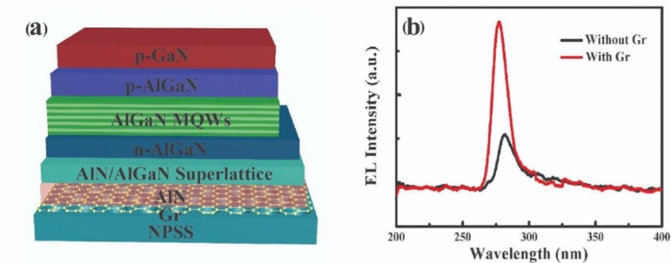
Multi-layer graphene improves epilayer quality, leading to more-efficient deep UV LEDs.

The addition of an indium-based underlayer traps surface defects, leading to a hike in internal quantum efficiency
Near-ultra-violet LEDs are plagued by a low external quantum efficiency that hampers development of white LEDs based on red, green and blue phosphors.
But this could all change, thanks to the work of researchers from EPFL and the Swiss Federal Laboratories for Materials Science and Technology. This partnership has shown that inserting an InAlN underlayer beneath a near-UV LED delivers a hike in internal quantum efficiency from below 10 percent to well over 60 percent.
Speaking on behalf of the team, Camille Haller from EPFL told Compound Semiconductor that indium is the key ingredient in the interlayer. The researchers think that this traps surface defects, preventing them from being incorporated in the active region, where they would lead to the creation of non-radiative recombination centres.
As yet, there is no theoretical support for this conjecture. “The role of the underlayer is highly debated, but we have already ruled out the impact of strain, the electric field, and screening of dislocations due to V-pit formation,” says Haller.
What is abundantly clear, however, is that the indium-containing interlayers are beneficial in nitride-based LEDs. “The striking feature is that all commercial blue LEDs feature an InGaN underlayer – bulk or superlattice – whatever the substrate is,” argues Haller.
Along with her co-workers, she has proven the benefit of InAlN underlayers in near-UV LEDs by making devices with and without this ternary, and comparing their performance. Samples were made by loading sapphire substrates into an Aixtron 200/4 RF-S MOCVD reactor and growing various epistructures, which all begin with a 2 µm-thick GaN buffer layer.
On top of this a 5 nm-thick layer of silicon-doped GaN is added in the control sample. Of the two variants, one features a 45 nm-thick layer of silicon-doped In0.17Al0.83N, followed by a 5 nm-thick layer of silicon-doped GaN; and the other has a superlattice, containing 24 interleaving pairs of 2.1 nm thick silicon-doped In0.17Al0.83N and 1.75 nm-thick silicon-doped GaN, followed by a 5 nm-thick layer of heavily silicon-doped GaN. Added on top of all three samples is an LED epistructure that features an active region with a single, 2.7 nm-thick In0.09Ga0.81N quantum well and a 20 nm-thick magnesium-doped Al0.2Ga0.8N electron-blocking layer.
All three types of epiwafer were processed into 300 µm by 300 µm LEDs, formed with a titanium and gold stack for the n-type contact and a combination of palladium and gold for the p-type contact.
Measurements of the internal quantum efficiency at a range of drive currents revealed a peak at 9 percent for the LED without the interlayer, and a maximum value of 21 percent for the chip with the bulk InAlN interlayer (see Figure). This moderate gain in performance is attributed to imperfections in the AlInN layer, which might be hampered by V-type pits.
One drawback of the bulk InAlN layer is that it leads to an increase in turn-on voltage – a bias of 3.26 V is required for a 20 mA current, compared with just 3.16 V for the control (see inset to figure). Polarisation mismatch at the second InAlN/GaN interface is thought to be the culprit, creating an electrostatic barrier.
The barrier is addressed with very high doping at the interface. This is employed in the LED with the superlattice – it has a smooth surface, high structural quality, and enables an internal quantum efficiency of 68 percent.
Haller says that the team will continue to work on understanding surface defects. Efforts will focus on comprehending the creation of these imperfections, and identifying them.
Reference
C. Haller et al. Appl. Phys. Express 12 034002 (2019)
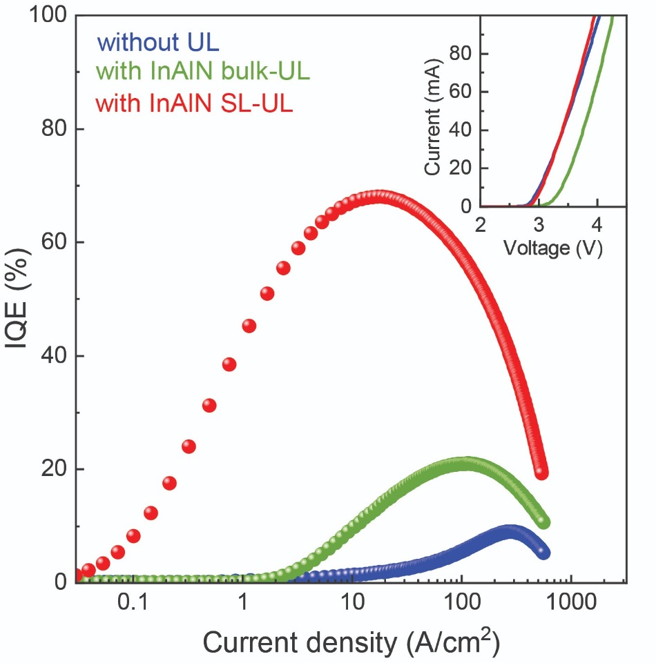
Placing an superlattice of InAlN and GaN underneath a UV LED boosts internal quantum efficiency without compromising the turn-on voltage

Cathodoluminescence reveals that sidewalls have a significantly lower magnesium content than standard GaN epilayers
Researchers from Arizona State University are claiming to have broken new ground by being the first to image lateral variations of magnesium doping efficiency in mesa structures.
This finding has implications for vertical GaN power devices, which are preferred for high-voltage, high-power applications, thanks to their high-voltage and high-power handling capability, good thermal management and compact design.
Fabrication of these devices involves the etching of epiwafers, followed by GaN re-growth on different planes. The magnesium doping in these devices must be uniform and high enough to pinch off the channel without any bias, and ultimately ensure normally-off operation. Based on this latest work, uniformity is challenging, given that different planes have different magnesium concentrations.
The researchers uncovered variations in magnesium doping concentration with cathodoluminescence (CL) measurements. Secondary ion mass spectroscopy (SIMS) could not have revealed this lack of uniformity, due to insufficient spatial resolution.
According to spokesman for the team, Fernando Ponce, the biggest challenge with their cathodoluminescence measurements is to correlate the luminescent characteristics with the magnesium doping in the control samples.
To carry out their investigation, the team used MOCVD to produce four different samples. The first is formed by growing a 4 µm-thick unintentionally doped layer of GaN, before using photolithography and chlorine-based inductively coupled plasma etching to produce a mesa structure, and then adding a 0.3 µm-thick unintentionally doped layer of GaN, followed by 1.65 µm-thick p-type GaN. The other three samples were produced by growing, on sapphire, a 1 µm-thick layer of n-type GaN, followed by a 1.65 µm-thick layer of p-type GaN. The difference between these samples is the flow rate for the source of magnesium, Cp2Mg – values of 50, 100 and 200 sccm created samples with differing p-type doping concentrations.
All four samples were annealed at 800 °C for 10 minutes to activate the magnesium doping. After this, the researchers used SIMS to determine the magnesium concentrations in the three planar samples.
Cross-sectional CL imaging and spectroscopy of the mesa structure revealed peaks at 2.9 eV, 3.25 eV and 3.4 eV, with relative intensity varying with location. These three peaks, which are seen in CL spectra from all three planar samples, have been observed by other groups. The peak at 3.4 eV has been attributed to near-band-edge excitonic transitions, while that at 3.25 eV stems from shallow-donor to magnesium-acceptor transitions, and that at 2.9 eV is associated with deep-donor to magnesium acceptor transitions.
By comparing CL spectra from the mesa structure to the spectra from the planar samples, the researchers concluded that the magnesium concentration in the upper mesa, the bottom of the lower mesa, and the centre of the lower mesa away from the sidewalls is about 3.1 x 1019 cm-3. That’s because the spectra resembles that from the sample produced with a Cp2Mg flow rate of 100 sccm. For the sidewall and the top of the lower mesa, the spectra is similar to that produced by the sample with a Cp2Mg flow rate of 50 sccm – it has a magnesium concentration of 1.3 x 1019 cm-3.
Reference
H. Liu et al. Appl. Phys. Lett. 114 082102 (2019)
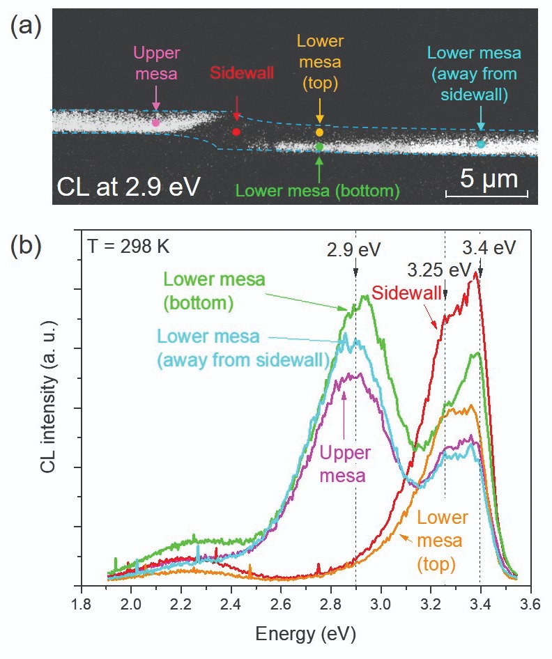
Cross-sectional optical properties of the mesa structure. Monochromatic cathodoluminescence mapping at 2.9 eV. (b) Spot-mode cathodoluminescence spectra in different regions in the p-GaN layer, as indicated by arrows in (a).
