


There’s a lot to be said for direct-emitting LED displays. Compared to the incumbents – LCDs and OLEDs – they definitely have the upper hand on two key fronts, efficiency and brightness. Those attributes matter a great deal today, as consumers want their devices to last a long time between charges, and have screens that can be read in bright sunlight.
Today’s displays do impress, however, when it comes to delivering a high resolution. Take the Apple retina line of products. They have more than 200 pixels per inch, a density that gives the iPad more than 3 million pixels.
It’s clear that maintaining this level of resolution with microLEDs will not be easy. The most popular approach involves parallel transfer of LEDs to ensure reasonable production times, but it’s going to have to be thousands of chips at a time.
That’s not the only headache. Placement must have micron-scale precision, and yield must be exceptional – dud pixels are completely unacceptable, and replacing them with ones that work is costly and time-consuming.
Fortunately, this is not the only approach to production. Offering an alternative is iBeam Materials, a spin-out of Los Alamos National Laboratory. It has developed a process for growing LEDs directly on a metal foil via an ion-beam assisted deposition process, which deposits a single-crystal intermediary layer (see p.18 for details).
On this layer iBeam’s engineers add a blue-emitting LED layer that can be processed into pixels, comprising three sub-pixels. Red and green sub-pixels are created by adding quantum-dot, down-converting layers – depending on the size of the LEDs, these colour converters can be added as a photoresist matrix, or with an inkjet printer.
To turn the pixels off and on, additional material is deposited and patterned to create an array of transistors above the LEDs.
There are many, many merits to this approach. For starters, the metal foil leads to a display that can bend, flex, and wrap around a curved surface.
What’s more, the cost of the technology is very promising. The use of metal foils enables roll-to-roll manufacturing. Use this in conjunction with a deposition process that supersedes MOCVD, and LED costs could fall so far that these displays would be cheaper than those based on OLEDs.
I know you know that there are many pitfalls in converting a promising technology into one that revolutionises an industry. But there is no doubt that iBeam’s approach has plenty of potential.

Welsh Economy Minister, Ken Skates has welcomed the European Commission’s approval of an innovative plan, spearheaded by Wales that identifies compound semiconductors as an important sector.
The plan will unlock €1.75billion of funding for research activities, will bring in up to Ä6billion in private investment and will ultimately help bring new technology innovations to market.
The overall objective of IPCEI is to deliver an integrated and collaborative approach to research and innovation to develop innovative components and technologies for use in applications including 5G communications, connected autonomous vehicles, and other next generation commercial and industrial devices.
It is expected to benefit both the Welsh and the wider UK economy by establishing South East Wales as the leading centre of compound semiconductor expertise.
The UK element of the pan-European joint microelectronics research and innovation project was driven by the Welsh Government and involves three Welsh companies: IQE, Newport Wafer Fab and SPTS Technologies (an Orbotech company), along with Manchester based ICS Ltd.
Economy Minister, Ken Skates said: “Wales’ semiconductor cluster and its contribution to many of the technologies that are so prevalent in our modern everyday lives is a real source of pride, and I am delighted Wales has taken the lead on behalf of the UK in co-ordinating this project that will drive vital research and accelerate innovation work across Europe.
“The EU’s decision to approve the plan is huge news for the sector and of course for Wales’ wider economy, paving the way for up to £6 billion of private investment throughout Europe and enabling our own semiconductor companies to work alongside international giants in their field.

“We look forward to working closely with our European partners and IQE, Newport Wafer Fab and SPTS on this exciting work and will do all we can to deliver the very best outcome for Wales.”
Commissioner Mariya Gabriel, in charge of Digital Economy and Society said: “Every connected device, every modern machine, all our digital services depend on microelectronic components that become smaller and faster with time.
If we don’t want to depend on others for such essential technology, for example for security or performance reasons, we have to be able to design and produce them ourselves. The decision to approve the project is a result of enhanced cooperation and shared European vision.”
The UK is already home to a number of state-of-the-art businesses and research facilities in the compound semiconductor space with a particular concentration in Wales. The South Wales semiconductor cluster – branded as CSconnected – is rapidly being recognised as a leading centre for enabling technologies powered by compound semiconductors.
The Commission’s approval of the project means that member states can provide up to €1.75 billion of funding for first deployment and innovation. This is expected to open doors to an additional €6 billion in private investment.
The overall objective of IPCEI is to deliver an integrated and collaborative approach to research and innovation to develop innovative components and technologies for use in applications including 5G.
Samsung Electronics has introduced the latest innovations in modular microLED display technology during its annual CES event at the Aria Resort & Casino in Las Vegas.
The new microLED technology designs featured at the event included: a new 75-inch display, a 219-inch The Wall as well as other various ground-breaking sizes, shapes and configurations for a next-generation modular Micro LED display – a 2019 CES Best of Innovation Award winner.
“For decades, Samsung has led the way in next-generation display innovation,” said Jonghee Han, president of Visual Display Business at Samsung Electronics. “Our microLED technology is at the forefront of the next screen revolution with intelligent, customisable displays that excel in every performance category. Samsung microLED has no boundaries, only endless possibilities.”
Featuring self-emissive technology and modular capabilities, Samsung’s microLED displays deliver high picture quality, versatility and design. These TV displays are made up of individual modules of self-emissive microLEDs, featuring millions of inorganic red, green and blue microscopic LED chips that emit their own light to produce brilliant colours on screen – delivering unmatched picture quality that surpasses any display technology currently available on the market.
At last year’s CES, Samsung introduced microLED by unveiling The Wall, the critically acclaimed, award-winning 146-inch microLED display. Due to the technical advancements in the ultra-fine pitch semiconductor packaging process that narrow the gap between the microscopic LED chips, Samsung has been able to create a stunning 4K microLED display in a smaller, more home-friendly 75-inch form factor.
Thanks to the modular nature of microLED, this technology offers flexibility in screen size that allows users to customise it to fit any room or space. By adding microLED modules, users can expand their display to any size they desire. The modular functionality of microLED will allow users in the future to create the ultimate display even at irregular 9×3, 1×7 or 5×1 screen sizes that suits their spatial, aesthetic and functional needs.
Samsung says its Micro LED technology also optimises the content no matter the size and shape of the screen. Even when adding more modules, Samsung Micro LED displays can scale to increase the resolution — all while keeping the pixel density constant. Additionally, microLED can support everything from the standard 16:9 content, to 21:9 widescreen films, to unconventional aspect ratios like 32:9, or even 1:1 – without having to make any compromises in its picture quality.
Finally, because microLED displays are bezel-free, there are no borders between modules – even when you add more. The result is a seamless, infinity pool effect that allows the display to elegantly blend into any living environment.
Twelve partners from northwestern Europe are creating an open access PIC (photonic integrated circuit) pilot line that it is claimed will drastically reduce costs and time for the pilot production of new products. This new facility is projected to be the incubator of a thousand new companies and thousands of jobs. The €14 million project (OIP4NWE) is supported by the European Regional Development Fund.
One of the main hurdles for PIC production is the high cost involved in R&D. Not only does it require expensive high-tech equipment installed in cleanrooms, but currently the production processes still have a high defect rate and are too slow. This was workable for basic research but not for commercial R&D.
The new project, led by photonics stronghold Eindhoven University of Technology (in collaboration with its Photonic Integration Technology Centre), consists of the realisation of an efficient pilot production line for shared use by European SMEs. It should take the defect rate in pilot production down and the throughput time will be shorter.
All in all, this should lead to a cost reduction which significantly lowers the threshold for developing new photonic products. This should help establish a thousand integrated photonics firms within ten years after the project.
The front-end process (production of PICs on InP wafers) will be realised in the existing NanoLab at Eindhoven University. The PICs of different companies will be combined on one wafer to keep costs low. The back-end process is done at the Vrije Universiteit Brussel (Optics for beam shaping and light coupling) and at the Irish Tyndall National Institute (Assembly of fibre-optic connections and electronics in the package). All steps require nanoscale precision to avoid product defects.
The first stage of the project is equipment installation. The second stage focusses on automation of the equipment while a third stage will involve intensive industrial research together with equipment manufacturers to optimise and develop new processes.
The line should be fully in operation in 2022. To incentivise the initial uptake by SMEs, a voucher scheme for external SMEs will be set up. The other parties involved are the companies Aixtron SE (Germany), SMART Photonics, VTEC Lasers & Sensors, Technobis Fibre Technologies (all Netherlands), mBryonics Limited (Ireland) and Oxford Instruments nanotechnology Tools (United Kingdom) along with research centres Photonics Bretagne (France), Cluster NanoMikroWerkstoffePhotonik.NRW (Germany) and Photon Delta Cooperatie (Netherlands).
The project has a total budget of €13.9 million. Of this, the EU is funding €8.3 million, with the remainder coming from the participating parties.
Osram Opto Semiconductors has announced an ultrafast laser driver with a high-power, multi-channel Surface Mount (SMT) laser for LiDAR (Light Detection And Ranging) systems. It has worked with GaN Systems to develop the technology.
One of the issues with LiDAR technology has been its inability to transmit lasers at short pulses, while maintaining high peak power, which is necessary to ensure that the LiDAR is eye safe with a long range and high resolution. To address this need, Osram worked with GaN Systems to develop a laser driver with a one nanosecond pulse rise time, while driving all four channels at 40 A each to deliver 480 W peak power.
This peak power then can be modulated at low-duty cycles to produce high resolution 3D cloud points at long range for new LiDAR designs. “Operating at the elevated current levels and nanosecond rise times necessary for long-distance LiDAR requires the high power, high frequency and robust thermal performance that are the hallmarks of GaN Systems’ products,” said Jim Witham, CEO of GaN Systems. “It is great to see the industry recognise these performance attributes and leverage them for its systems.”
Scanning LiDAR is a key technology for Advanced Driver-Assistance Systems (ADAS), which is designed to increase road safety and enable autonomous driving. These electronic devices react instantly to potential collisions without wasting precious seconds of reaction time. Scanning LiDAR creates high-resolution 3D images of a car’s surroundings and registers obstacles early enough for ADAS or self-driving cars to initiate the appropriate driving manoeuvres, such as automatic braking to prevent collisions.
“Osram enables LiDAR technology for autonomous vehicles by not only developing high power, multi-channel SMT lasers that meet automotive quality standards, but also working with eco-system partners like GaN Systems to address the technological barriers that arise”, said Rajeev Thakur, senior marketing manager at Osram Opto Semiconductors. “Our lasers are leading the way to make autonomous driving a reality for everyone.”
Osram has continuously expanded its laser portfolio for LiDAR to accommodate the needs of customers, including increasing the peak power of the SPL DS90A_3 to 120 W at 40 A. In addition, Osram plans to release a four-channel SMT laser in 2019. The additional channels increase the field of view and total peak power, with each channel being capable of generating 120 W.
EPC has announced the successful AEC Q101 qualification of two additional eGaN devices, addressing a range of applications in the automotive industry and other harsh environments. The new products, EPC2206, and EPC2212 are both discrete transistors in wafer level chip-scale packaging (WLCS) with 80 VDS and 100 VDS ratings respectively.
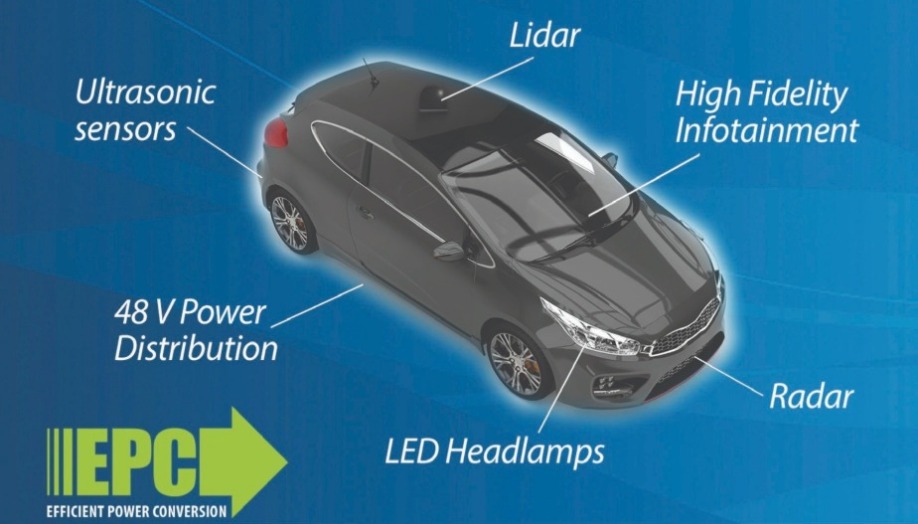
eGaN technology has been in mass production for over eight years, accumulating billions of hours of successful field experience in automotive applications, such as LIDAR (Light Detection and Ranging) and radar for autonomous cars, 48 V - 12 V DC-DC converters used in data centre computers, ultra-high-fidelity infotainment systems, and high-intensity headlamps for trucks. These new devices have completed rigorous automotive AEC Q101 qualification testing and will be followed with several more discrete transistors and integrated circuits designed for the harsh automotive environment.
The EPC2206 is an 80 V, 2.2 mΩ enhancement-mode FET with a pulsed current rating of 390 A in a 6.1 mm x 2.3 mm chip-scale package. The EPC2212 is a 100 V, 13.5 mΩ component with a pulsed current rating of 75 A in a 2.1 mm x 1.6 mm chip-scale package. These eGaN FETs are many times smaller and achieve switching speeds 10 - 100 times faster than their silicon MOSFET counterparts.
The EPC2206 device is suited for vehicles using 48 V bus power distribution to manage the power-hungry electronically-driven functions and features appearing on the latest cars. Electric start-stop, electric steering, electronic suspension, and variable speed air conditioning are a few examples. And now, with the emergence of self-driving vehicles, additional demands from systems such as LIDAR, radar, camera, and ultrasonic sensors are placed upon the power distribution system accelerating the need for automobiles to move to a 48 V bus system. For 48 V bus systems, GaN devices like the EPC2206 increase efficiency, shrink size and weight and reduce system cost.
The EPC2212 is designed for firing the lasers in LIDAR systems because the FET can be triggered to create high-current with extremely short pulse widths. The short pulse width leads to higher resolution, and the higher pulse current allows the LIDAR system to discern objects at greater distances. These two characteristics, along with their tiny size and low cost, make eGaN FETs ideal for radar and ultrasonic sensors in addition to LIDAR in demanding automotive applications.
EPC’s CEO and co-founder Alex Lidow notes: “These two automotive products are the next in what will be a constant stream of transistors and integrated circuits designed to enable autonomous driving and improve fuel economy and safety. Our eGaN technology is faster, smaller, more efficient, lower cost, and more reliable than the ageing silicon power MOSFET used in today’s vehicles.”
The Compound Semiconductor Centre (CSC), IQE’s joint venture with Cardiff University, and its partners (SPTS Technologies, Cardiff University and Swansea University) have announced the successful conclusion of an Innovate UK funded project – ‘High Efficiency Manufacturing of Vertical Cavity Surface Emitting Lasers (VCSELs)’.
The project has delivered key process modules required to transition small diameter manufacturing processes currently used for VCSELs to a high uniformity 150 mm epitaxial platform. The need for scale-up is driven by significant benefits in terms of productivity “(four times more die sites in transitioning from 75 mm to 150 mm ) and yield (driven by smaller ratio of edge sites to total area for larger wafer diameters) to facilitate a step change in cost reduction for VCSELs, and thus accelerate adoption in mass market applications such as 3D imaging, proximity sensing, range-finding and LIDAR.
The work included the commissioning of a custom 150 mm oxidation tool at Cardiff University’s Institute for Compound Semiconductors which is used for a particularly challenging stage of preferential oxidation of aluminium rich layers in the VCSEL layer structure, to produce a high efficiency optical waveguide in the device. High quality mesa dry etch processes to >5 μm were developed by SPTS on GaAs/AlGaAs epitaxial structures supplied by CSC, with Swansea supporting PECVD and photo process steps, to complement the oxidation process module; essential for a high uniformity, high reliability 150 mm VCSEL fabrication platform.
A robust process solution was developed, including in-situ depth targeting end-point detection capability. A benchmark of <±5% mesa depth uniformity across a full 150 mm VCSEL epitaxial wafer structure was demonstrated.
The capability will form the core of a future 150 mm VCSEL prototyping capability which will be leveraged by the consortium to work on custom VCSEL development, device-scale optimisation and validation of VCSEL epitaxial materials development as a core research and manufacturing competence in the emerging CSconnected Compound Semiconductor Cluster in South Wales.
Akash Systems, a company focused on next generation mini satellites, has been granted an Experimental Special Temporary Authority (STA) license from the US Federal Communications Commission (FCC) for a satellite launch featuring its proprietary GaN-on-diamond transmitter technology. The G aN-on-diamond technology will be integrated into a Ka-band (17.2 to 20.2 GHz) 3U radio transmitter and launched in a 12U CubeSat allowing for new levels of data transmission for customers to increase capacity and reduce end-user costs.
“Taking the lead in the satellite communications industry, this demo will showcase the use of our proprietary GaN-on-diamond Radio Frequency (RF) amplifier technology,” said Co-founder, CEO and GaN-on-diamond Inventor Felix Ejeckam. “Beyond the capability to handle the increasing demands of today’s extreme data throughput, we are confident future adoption of the system will drive down end-user costs to levels never before seen.”
The company’s satellite launch will demonstrate the transmitter’s capability to handle more than 5 Gbps downlink speeds from a 10 W 3U radio transmitter. Tentatively slated for early 2020, the launch will validate the data rates, reliability and space-qualification readiness of the GaN-on-diamond transmitter technology. The new technology enables a smaller, lighter and higher performing satellite that will pave the way to lower launch costs, reduced cost-per-bit, more launch cycles, and increased communications access around the earth.
“Anyone buying our solid-state power amplifiers (SSPAs) to transmit data to or from space will be interested in the space worthiness and reliability of our SSPA products,” said Jeanette Quinlan, director of space systems, Akash Systems. “This launch helps us capture that worthiness and reliability data for them.”
Akash will continue to focus on scaling up and qualifying its GaN-on-diamond Power Amplifier product line, offering customers products with higher frequencies that will be announced in the months ahead. The picture above is an artist’s rendering of Akash Systems’ McNair 12U CubeSat.
Photo Credit: Blue Canyon Technologies
Mitsubishi Electric has announced the ML562G86 pulse laser diode for projectors, featuring a vibrant 638 nm red light, world-record output power of 3.0 W under pulse operation and mean time to failure (MTTF) of over 20,000 hours.
The ML562G86’s high output power and wide operating temperature range will contribute to enhanced projector luminance and miniaturisation. Sample sales began on January 11, 2019 and volume shipping will begin in April 2019.
Projector light sources are shifting from mercury lamps to solid-state light sources that offer wall-plug efficiency, a wide colour gamut, and highly reliable operation. LDs achieve the best wall-plug
efficiency among solid-state light sources, thereby contributing to lower power consumption, and thus are viewed as the most promising new light source for projectors. Mitsubishi Electric expects to use laser diodes to develop not only superior projectors but also advanced laser TVs capable of more vibrant images than liquid-crystal TVs.
In September 2015, Mitsubishi Electric released its ML562G84 high-power red laser diode, which achieved 2.5 W output under pulse operation as a red laser diode in three RGB light sources for projectors. With conventional laser diodes, extended operation at 3.0 W output power causes the laser’s light-emitting surface crystals to melt, making it difficult to achieve an MTTF of 20,000 hours. In response, Mitsubishi Electric has developed the technology required to suppress degradation of the light-emitting surface even at 3.0 W, leading to the newly announced ML562G86 red laser diode that achieves unprecedented 3.0 W output power.
An October 2018 vote on proposed water guidelines in Europe ruled in favour of more stringent quality standards for consumer drinking water, expanding monitoring and limits on certain pollutants, including legionella. Now Crystal IS, a developer of high-performance UVC LEDs, has announced independent testing results of the Klaran AKR, an on-demand UVC LED-based water disinfection reactor designed by Asahi Kasei Corporation, the parent company of Crystal IS, intended for consumer and commercial water purification. Performed by the University of Colorado Boulder, testing showed the AKR reactor provided 99.998 percent reduction of legionella pneumophila at a flow rate of two litres per minute.
The recently passed Revision of the Drinking Water Directive in the European Union notes that legionella causes the highest health burden of all waterborne pathogens in the Union and proposes to apply random monitoring at the tap to man-made water systems and subsequent remediation actions to improve water safety. The performance of the Klaran AKR would provide an immediate risk management solution for meeting the <1000 CFUs/Litre assessment value. “UVC LED technology enables water product manufacturers to differentiate their solution with point-of-dispense disinfection, supporting new and existing customers in mitigating the risk of legionella,” said James Peterson, product manager, Crystal IS. “The Klaran Reactor series uses our UVC LEDs to provide maintenance-free disinfection that lasts longer and is more affordable than UV lamps or filtration cartridges. Along with its compact size, this makes the Klaran AKR an ideal method of worry-free legionella management.”
Enforcing regular monitoring at the point of dispense would not only improve water hygiene from large and small utility systems, but also promote new risk identification mechanisms inside of building distribution systems and water holding appliances. In addition to potentially improving public health, raising consumer confidence and reducing cases of Legionnaires’ Disease, this regulation would place increased accountability for water hygiene on building managers and water product designers in the European Union.
While individual Member States, system operators, and building managers will need to interpret their risk reduction plans based upon the final legislation, water purification and appliance manufacturers are acting on these future needs now to provide new solutions for this existing health concern and upcoming regulatory situation. Lasting for years after installation rather than months, Klaran reactors provide effective water hygiene without maintenance schedules or burdens to owners and service providers. As both facilities and product designers face the task of identifying low impact strategies to improve legionella management, Klaran UVC LED-based reactors will offer long term and unobtrusive installation into water systems, while providing reliable performance claims backed by third party validation. Klaran AKR reactors are available for design integration sampling now.
Aixtron has announced that the Taiwanese microLED firm PlayNitride, will receive an AIX G5+ C MOCVD system for the manufacturing of GaN-based microLEDs. They companies have also signed a joint collaboration agreement to technically and commercially work together.
microLED technology is a major challenger to existing display technology for next-gen consumer products. Displays made of microLEDs consist of micron-sized LED arrays forming individual sub-pixel elements. Compared to the existing LCD and OLED technologies, microLED displays offer lowest power consumption while exhibiting superior pixel density, contrast ratio and brightness. Thus, opening new horizons for consumer mobile products as well as premium TV displays.
PlayNitride has chosen the AIX G5+ C for microLED MOCVD processing. Aixtron’s advanced production tool is said to offer market leading wavelength uniformity to meet the tightened microLED market specifications in a batch reactor high-throughput environment. Furthermore, the system is designed to allow for very low defect and particle levels due to an effective in-situ cleaning technology and the cassette-to-cassette handler which is essential for high yields.
“We are very pleased that PlayNitride as a key player in the business has selected the AIX G5+ C for the further development of groundbreaking microLEDs production processes. We are looking forward to our joint collaboration to accelerate a breakthrough in the commercial and technical use of microLEDs for displays. Our AIX G5+ C platform perfectly backs PlayNitride’s product strategy since it allows for outstanding performance in a high-volume manufacturing environment”, comments Bernd Schulte, president of Aixtron.
Taiwan-based PlayNitride was established in June 2014 to research and develop Nitride related materials and applications. The company is now focusing on GaN-based microLEDs - it is branding its technology as PixeLED displays and has recently demonstrated microLED display prototypes.
In April 2018 Taiwan’s Ministry of Science and Technology approved PlayNitride’s application to setup a $17 million production facility at Hsinchu Science Park. PlayNitride aims to produce microLEDs, display modules and panels at its new facility at Hsinchu.
Will Infineon’s acquisition of Siltectra secure SiC wafer supply for the German semiconductor manufacturer, asks Rebecca Pool.
In a bid to guarantee materials supply, Infineon bought Dresden-based start-up, Siltectra, for €124 million, last month.
At a time when shortages in SiC wafer supplies rumble on, Siltectra has developed a novel technology – ‘cold splitting’ – to process crystals with minimal materials loss.
The technology is used to split SiC wafers and double the number of chips produced from one wafer. Importantly, Infineon now hopes to industrialise this process.
As Peter Friedrichs, Infineon’s senior director of wide band gap semiconductors, puts it; “A huge motivation for this acquisition is security of supply and production ramp capability.”
“Given the silicon carbide shortage of supply, especially with 150 mm wafers, we just want to make sure that if this continues, we are able to still deliver to customers,” he adds.
Founded in 2010, Siltectra has spent the last eight years developing its wafer-splitting process and building a solid patent base. The spalling process uses externally applied stresses to separate crystalline materials along crystal planes with a well-defined thickness.
A laser defines a layer within the crystal to a predefined depth, with a custom polymer foil then deposited onto the top of the material. This materials system is then rapidly quenched to around -160 °C to induce enough stress to mechanically split the material along its laser-defined layer, separating a wafer from the rest of the boule. The polymer foil can then be removed from the new wafer by standard wet-chemical cleaning. And, importantly, the remaining crystal boule can then be prepared for the next ‘bonus’ wafer, vastly reducing manufacturing costs.
Materials gains aside, cold-splitting promises other benefits. As Friedrichs highlights, the mechanical stresses from traditional wire-saw processes far outweigh those imposed by cold-splitting, so the new process yields wafers with fewer defects.
What’s more, the process can also be used on GaN, GaAs and sapphire wafers, although Infineon intends to focus on SiC in the next few years.
But crucially, results to date indicate that the process can thin wafer materials to 100 μm and below in minutes with high precision and virtually no material loss, a feat that Infineon now intends to repeat at production scale.
“Right now, we have a proof-of-concept, laboratory scale process, so we now need to scale up and automate the process to run with high throughput, twenty four hours a day, seven days a week,” says Friedrichs. “As part of this, we need to define the equipment for a mass manufacturing process from scratch, as there is nothing else that is out there.”
“You know, the company in Dresden is a start-up, has used demonstrator tools and sometimes even home-made equipment,” he adds. “The challenge for us is that there is nowhere to order new equipment for scale, so we are now partnering with companies that can manufacture the necessary production equipment that can be implemented into an automated manufacturing set-up.”
All in all, the company estimates that the transfer to volume production will be completed within the next five years. Industrialisation is set to take place at Siltectra’s existing Dresden site as well as Infineon’s SiC manufacturing site and headquarters in Villach, Austria.
According to Friedrichs, final SiC chip production will take place at Villach, and Infineon will not create an additional manufacturing site at Dresden. “As an intermediate situation, we might also use Dresden for some initial pre-production trials,” he says. “But the plan is to use the Dresden facility for alternative development in other directions.”
Proving the process
Earlier this year, Siltectra revealed it had produced GaN-on-SiC HEMT devices on split-off wafers, with Friedrichs confirming Infineon has also fabricated practical devices. And with question marks still hanging over the supply of SiC wafers – only a few months ago industry analyst firm Yole Développement confirmed the supply bottleneck remained – Infineon’s latest acquisition looks set to ease the ramp-up of SiC devices.
“The biggest motivation for this has been to increase the availability of SiC material,” emphasises Friedrichs. “With cold-splitting we can simply double the number of wafers that we have allocated to our long-term agreements with suppliers.”
“This is our first counter-measure to tackle the materials shortage problem and is part of our long-term strategy to roll out technologies relating to silicon carbide,” he adds.
Japanese UV-LED manufacturer, Nitride Semiconductor, claims to have developed an easy way to make micro-LEDs for better performing displays. Rebecca Pool finds out more.
LAST November, Japan-based UV LED manufacturer, Nitride Semiconductors, set-up a
100 percent owned subsidiary, Micro Nitride, to develop and manufacture micro UV-LED chips for micro-LED displays.
Initially targeting flexible displays for next-generation smartphones, Nitride Semiconductors is ploughing 100 million yen – nearly £700,000 – into its new venture and expects displays to reach commercial markets come 2020.
“LED prices are coming down and down, and Chinese companies are getting bigger and bigger,” says Nitride Semiconductors president and chief executive, Yoshihiko Muramoto. “Japanese LED makers are now in a difficult situation and need to add value, we need to make displays and not just LEDs, so we have established our new company.”
Nitride Semiconductors unveiled its first UV LED in 2000 and has since delivered myriad wafers, chips and modules to UV LED markets worldwide. Its new subsidiary will now produce micro UV-LED chips that comprise the micro UV-LED and a red, green, blue (RGB) phosphor to generate ‘natural’ white light.
Importantly, Muramoto reckons this UV-LED and RGB phosphor approach eases chip manufacture and leads to better-performing displays than existing methods. Today’s fledgling micro-LED displays have typically been manufactured with red, blue and green LEDs or a blue LED that excites red and green phosphors.
However, many issues have stymied development. Take the RGB microLED array; mounting different semiconductor structures at high density isn’t easy. What’s more, current, voltage and response speeds vary from LED to LED, complicating chip control.
Meanwhile, for the micro blue LED excitation method, only the blue light is directly emitted while the red and green light result from phosphor conversion with an associated time lag.
“Synchronising the colour response can be very complicated and we just don’t have to manage any time lag,” says Muramoto.
“Our micro UV LEDs are also easy to mount and we have a fifty year history of using phosphor; it is very natural for us to use UV LEDs for displays and lighting.”
The new subsidiary will focus on technology development, rather than manufacturing. As Muramoto puts it: “Japanese companies should aim to develop strong technologies and patents... there are many big LED manufacturers around the world and we can outsource our technology to them.”
And with the technology in tow, the chief executive says his company’s micro UV-LEDs are ready for mass manufacture, claiming fabrication is ‘not so difficult’. Importantly, his company is also working with Japan-based display supplier, V Technology, on display manufacture.
Pick and place pains
MicroLED displays have been notoriously difficult to manufacture, using traditional pick and place transfer processes in which each sub-pixel is placed onto a CMOS backplane one at a time.
Given this, many companies have been working on mass transfer manufacturing processes, including
V Technology. In such a process, thousands of sub-pixels are simultaneously moved from a sapphire or silicon donor carrier to the display substrate. While Muramoto will not disclose details of V Technology’s mass transfer process, he emphasises: “[The company] can manufacture these displays relatively easily and they will be ready for market in two years.”
In the meantime, the chief executive is confident that come mass production, final display costs will appeal. “We are going to need huge volumes of UV LED chips... but with our micro UV-LED method, we can simplify the structure of the display and the mass transfer process will be relatively easy.”
Importantly, Nitride Semiconductors is also in close contact with smartphone manufacturers, which is where Muramoto is certain the micro-LED display action first lies.
He reckons the final cost of a display panel for a smartphone will be around $50. In contrast, he claims the cost of a similar panel, made using other methods, will be as high as $400.
“The merit of the micro-LED display is that it is flexible,” he says. “So microdisplays should be used for wearable applications and we are talking with smartphone manufacturers about this [for next-generation devices].”
“Our technology is not so complicated and has been very easy to realise,” he adds. “Our competitors have been struggling, but we can get good results.”

To mark the end of 2018, Transphorm revealed that it had shipped more than 250,000 high-voltage GaN FETs, which co-founder and chief operating officer, Primit Parikh, believes is testament to rapidly accelerating GaN market adoption.
As he tells Compound Semiconductor: “2018 has been a game-changing year for high voltage GaN and we finally believe that the last several years of effort that have gone into GaN are now materialising very quickly.”
“Our 650 V GaN FETs are deployed in customers’ mass production, high-performance power converters,” he adds. “We’re already in data centre and industrial sectors, and expect more market penetration in areas such as consumer adapters, as well as volume ramping in these markets.”
Crucially for Transphorm, recently available field failure data indicates that products are reliable. According to Parikh, his company’s GaN FETs now have more than 1.3 billion field hours of operation with low ‘failure in time’ rates.
“This is very exciting and it’s the first time Transphorm, or any supplier, has comprehensive field failure data,” says Parikh. “These statistics only become meaningful at more than a billion hours, so this is a significant milestone for us and also increases customer confidence in GaN.”
Without a doubt, solid reliability data can only drive Transphorm’s GaN devices further into more applications. Key customers include US-based power supply manufacturer, Bel Power Solutions, Japan-based servo motor manufacturer, Yaskawa Electric, computer peripherals supplier, Corsair, US, Taiwan-based computer power supply maker, Seasonic Electronics and solar/electric power generator developer, Inergy, from the US.
According to Parikh, data centres will continue to be a key market for Transphorm, given the rise in edge computing and hyperscale data centres.
And the company will also target adapters for consumer supplies.
“There is a huge push to increase power density for power levels ranging from 65 W to 150 W within existing form factors, which silicon cannot achieve. GaN can do this,” he says.
The chief operating officer also has high hopes for automotive markets. Last year, Transphorm delivered the world’s first AEC-Q101 qualified GaN transistor, which at 650 V targeted AC-DC conversion for electric vehicle on-board chargers as well as auxiliary high voltage DC-DC conversion in air conditioning, heating power, steering and oil pumps.
“This paradigm shift to electric vehicles has been so large and from when we first started sampling, customers have really been pulling us in,” say Parikh.
Parikh won’t be drawn on specific customers but also highlights strong demand from Japan-based automotive manufacturers that want to fit higher power DC-AC power inverters into vehicles.
“The Lexus, for example, has a 400 W AC power plug but now people want more power with 1.5 kW becoming the norm in brand new vehicles,” he says. “GaN can provide the size, weight and thermal performance that is so important here.”
Parikh is also certain that Transphorm’s stake in the Fujitsu-owned wafer foundry at Aizu, Japan, had been instrumental to fuelling demand there.
“The Fujitsu factory has given us a strong Japanese market presence,” he points out. “It has a good reputation as a long standing supplier of silicon products to the automotive sector, has proven GaN production, and has the ability to scale to volumes; this has all helped a lot in these automotive markets.”
And in the longer-term, Parikh also hopes to target the mighty drivetrain inverter in electric and hybrid vehicles. “This is a more conservative application but GaN can certainly address its needs,” he says.
Scaling manufacture
Rising demand dictates rising volumes, and Transphorm is set to scale. Recently claiming that device volumes can be ‘easily’ increased by a factor of five, Parikh also asserts that the transition from 6-inch to 8-inch wafer production will not be difficult when the market demands it.
“Our ability to scale is strongly linked to the fact that we are a vertically integrated business,” says Parikh. “In addition to MOCVD, our Aizu wafer foundry is also a silicon-based foundry, set up for huge volumes of silicon so there is lot of equipment here; we can scale when the need comes as the necessary infrastructure is already in place.”
Parikh is also confident that the industry supply chain is now in place, which he claims, may actually place GaN in a better position than rival technology SiC.
“We start with silicon substrates and GaN can run in any existing silicon fab, with the necessary expertise in place,” he says. “But look at the overall supply chain for silicon carbide; we see a few companies [including Wolfspeed, Infineon and Rohm] making the silicon carbide substrate, but we are also seeing shortages here, and this is limiting the supply chain.”
According to Parikh, in key applications the performance of 650 V GaN devices already surpasses that of SiC, at a lower price point. “So now our goal is to provide GaN devices with better performance than SiC but approaching silicon-like prices,” he adds.
Transphorm’s volume production plans also come at a time when Infineon has just unveiled its first GaN products, 600 V HEMTs with drivers, for adapter, wireless charging and server applications.
The launch makes Infineon the only company, right now, to offer all power electronics technologies – silicon, SiC and GaN – and, like Transphorm, the Germany-based semiconductor manufacturer is ready for volume production.
Parikh isn’t fazed. As he puts it: “More and more companies are either joining the market or have announced ambitions to do this, and companies such as Infineon and Nexperia joining us is great news for GaN as it boosts customer confidence.”
“Just as we saw with GaN LEDs, more companies are joining the marketplace and a core set of strong companies, with the strong technologies and IP, will now dominate the market for a few years,” he adds. “This includes us, and the ride is just about to begin.”
Transphorm 650V GaN FETs are deployed in a range of customers’ mass production power converters.
“Infineon and Nexperia joining [the market] is great news for GaN as it boosts customer confidence.”
The manufacture of microLED displays can take a big step forward by switching to the monolithic integration of transistors and LEDs grown on metal foils
BY VLADIMIR MATIAS AND JULIAN OSINSKI FROM IBEAM MATERIALSEvery year, billions and billions of LEDs are made by growing epitaxial layers of GaN and its related alloys on sapphire and silicon substrates. But that’s not the only option. At iBeam Materials of Santa Fe, NM, we have recently demonstrated that high-quality epitaxial GaN can also be deposited on polycrystalline flexible metal foils. Our technology opens the door to large area, lower-cost production of GaN-based devices with a process that is amenable to roll-to-roll manufacturing.
The approach that we employ involves ion-beam-assisted deposition. It is used to deposit a single-crystal-like intermediary layer, which forms the foundation for subsequent epitaxy of nitride layers. Working in partnership with researchers at Sandia National Laboratories and the University of New Mexico, we have used this technology to demonstrate practical LEDs through a project funded by the US Department of Energy, APRA-E (see Figure 1).
One of the more attractive opportunities for our ground-breaking technology is in microLED displays, which require large areas of low-cost LED arrays. The most common approach to making these arrays is based on singulation and mechanical transfer. However, there is a move to ever smaller LEDs, making this technique more challenging to implement. It is far better to adopt a monolithic integration approach, which is compatible with our technology.
The microLED market is expected to be huge as it takes market share from LCDs and OLEDs due to the significant advantages that this class of display has over the incumbents. MicroLEDs are brighter and much more efficient, so displays can be read in direct sunlight, and products using batteries will last longer between charges. What’s more, these products will provide a longer display lifetime, given the tremendous reliability, lifetime and robustness of the inorganic LED.
Thanks to all these strengths, microLED-based displays should rapidly replace OLED and LCD screens in wearables, cell phones and augmented reality. But this is only the start: LEDs are destined to go on and have success in larger displays as well.

Figure 1. iBeam Materials’ GaN-on-metal technology relies on a single-crystal-like layer that is created on top of a polycrystalline substrate, such as a long-length metal foil. The single-crystal-like layer is formed by an ion-beam-assisted deposition process. On the left is shown the layer architecture, while photographs show the first LED devices.
With the conventional approach to making large-area microLED-based displays, there is a need to use a high-yield process that provides massively parallel transfer of individual LED chips that may be less than ten microns in size. High-definition displays contain 1080 by 1920 pixels, so they require 6.2 million red-green-blue subpixels. And in a 4K display, there are nearly 25 million subpixels. These numbers are so high that in order to minimize the number of transfer steps, LEDs have to be transferred in many thousands at a time.
Several companies are developing technologies for handling in parallel such large groups of LEDs, which could have dimensions down to just 3 μm. These approaches have to transfer chips with micron-scale precision, bond them reliably, and realise an incredibly high yield. Even 99.99 percent will not be good enough, as the display could still contain thousands of dead subpixels. They would have to be repaired, because the market will not tolerate even a single malfunctioning or missing pixel in a new device.
Repairing individual pixels is an option, but costs escalate, as this requires additional transfer steps. So it may be better to resort to redundancy in transferring. However, this adds significantly to the LED cost, and it fails to address the problem head-on.
In contrast, we tackle this issue with a technology that can make a paper-thin flexible product with a resolution of 500 pixels per inch or more, and satisfy the market’s tremendous desire for integration of displays into thin, curved devices. Using patented GaN-on-metal technology, we grow LED-quality InGaN material directly onto low-cost, large-area flexible metal foil, making monolithic integration of microLEDs practical.
This foil allows our displays to be as good as or better at conforming to curved surfaces than OLEDs. In addition, they may even be able to flex when in use. The conformable metal substrate also provides reflectivity and heatsinking for the LEDs (see Figure 2).

Figure 2. Diagram of an LED cross section, and emission from a 20 μm blue LED on metal and an array of microLEDs
$2-3/cm2, but they could fall by a factor of three by switching to long-length metal substrate. Further savings will result from the introduction of non-MOCVD deposition processes – our cost model estimates an epi-material cost reduction of more than a factor of ten per unit area (see Figure 3).
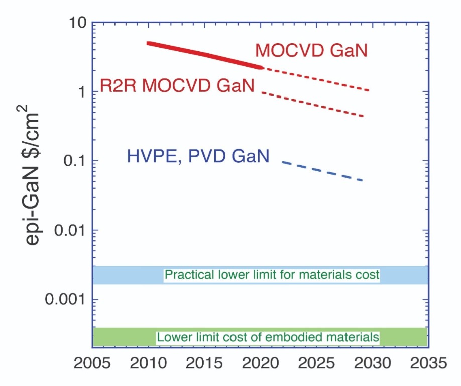
Figure 3. Cost curves of epi-GaN device layers for various deposition methods.
Fabrication of our full-colour, active-matrix display begins by producing a dense array of blue-emitting LEDs monolithically across the surface of the epilayers. Each pixel comprises three sub-pixels, with red and green components formed by coating blue-emitting elements with quantum-dot down-converting layers (see Figure 4). They can be added as a photoresist matrix, or with an inkjet printer, depending on the size of the LEDs required.

Figure 4. The layout of a microLED display made using iBeam technology.
The next step is to add a thin-film transistor circuit to address each of the sub-pixels. We are able to draw on the existing backplane technology used to make OLED displays, with thin-film materials deposited on the sheet, prior to patterning (see Figure 5).
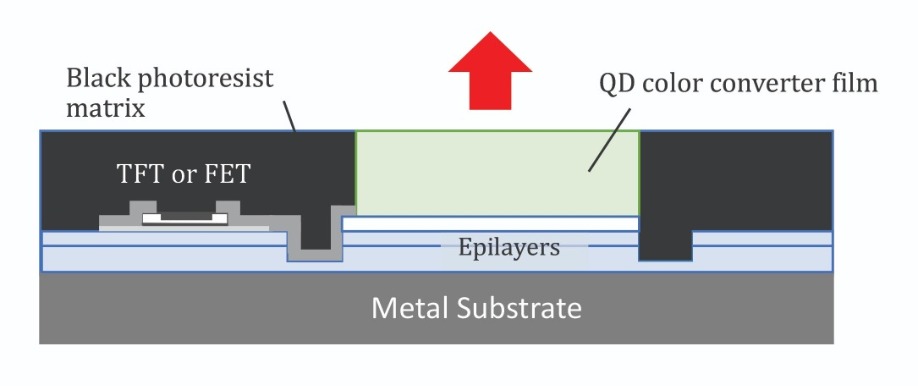
Figure 5. A sub-pixel cross-section showing a quantum-dot, colour-converting film and black photoresist matrix.
Our technology will continue to advance. In future, we will use the epitaxial GaN sheet that exists on the metal foil to fabricate small, integrated GaN transistors. These devices can be used to control the LEDs (see Figure 6).
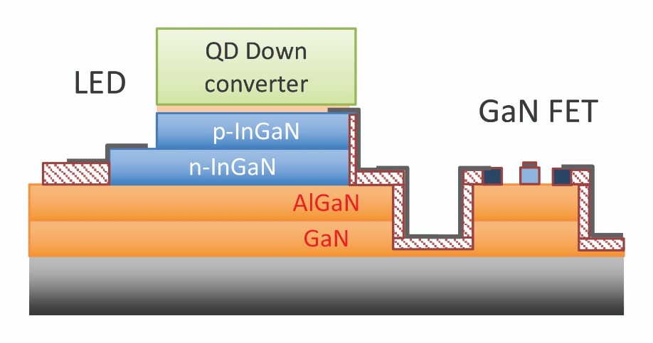
Figure 6. The sub-pixel LED can be integrated with an GaN/AlGaN FET transistor device, by integrating the FET in the epi structure.
We are confident that over time, the yield and reliability of microLED displays made with our technology will be far higher than those made with chip-transfer methods. However, to begin with, it may be prudent to utilize some redundancy in design, in order to minimize possible LED failure.
When there is a move to higher-resolution displays, our technology is well-positioned – thanks to the complete area being filled with LED epi, higher resolution displays can be made with smaller additional costs. For our monolithically integrated LED display technology, cost scales with area, rather than the number of pixels.
Our approach is not the only one providing monolithic integration. One alternative involves nanowire active regions. However, this relies on conventional rigid substrates, such as silicon and sapphire. Go down that path and the manufacture of large-area displays tends to require the transfer and bonding of LEDs to a backplane.
Colour and gamut
The quantum dot technology that we are advocating to make our displays is advancing, with today’s films with a thickness of just a few microns providing nearly full conversion of blue emission to that in the red or green. However, if there are concerns relating to any unwanted blue light that remains in the sub-pixel spectrum, it can be removed with a filter or blue reflector.
Makers of displays can choose the quantum dot films to hit specific colour points. The narrow emission of the LEDs and the quantum dots – they have spectral widths of typically 20 nm and 30 nm to 40 nm, respectively – enables saturated colours, along with colour gamuts that are wider than those of conventional LCDs and OLEDs (see Figure 7 for further details).
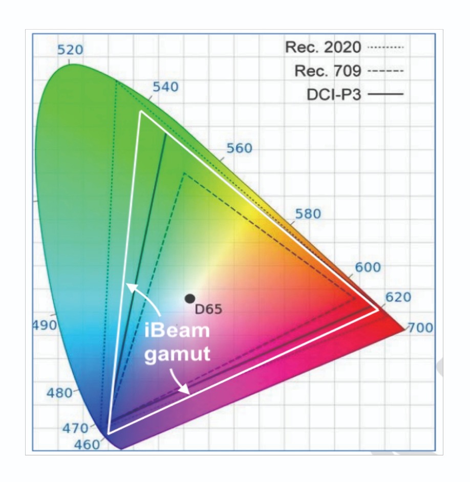
Figure 7. Three popular gamut standards are targets for new products.
Rec. 709, also called sRGB, is the current HDTV standard. However, products such as the Apple iPhone and Samsung Galaxy have already moved to embrace DCI-P3, the digital cinema standard, and future products are targeting the most difficult laser-based Rec. 2020 standard. iBeam technology will be capable of exceeding DCI-P3 and nearly meeting that of Rec. 2020 without requiring lasers.As the microLED market expands, there is a need for a roll-out of significant additional LED manufacturing capacity in order to make all the required displays. By 2026, some forecasts show 15 percent of the 2 billion cellphone market will feature a 4K microLED display. This alone will require 12 million wafer starts per year, a figure comparable to the total for all LEDs that will be manufactured in 2019. Factor in wearables, TVs, and other display formats, and manufacturing volumes are set to be far higher than this figure.
Our low-cost, roll-to-roll capability can make this ramp possible. Just one wide-web, roll-to-roll production facility could equal today’s total worldwide LED epi production.
Beyond 2025, displays based on two-dimensional flat screens are expected to be superseded by those that create images in a three-dimensional space (see Figure 8). This can be accomplished by placing an array of emitters, such as microLEDs, over a microlens array. However, to ensure that the light-field display has a high resolution, in addition to compression of huge amounts of data, it must feature billions of pixels with a pitch that could be as small as 5 μm. Such a colossal number of pixels is impractical for mass transfer approaches, but can be realised with our monolithic integration technology.
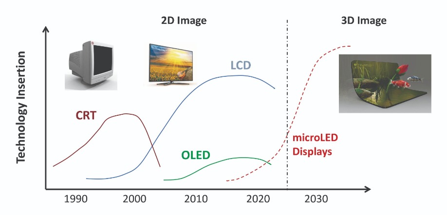
Figure 8. Historical evolution of displays and expectations into the future.
Further reading
United States Patent 9,735,318 B, V. Matias and C. Yung.
V. Matias, Photonics West Presentation, 2018
Yole Développement, “Are MicroLEDs a credible alternative to LCD and OLED?” SID Display week business conference, (2018)
G-S. Chen et al. IEEE Phot. Tech. Lett. 30 262 (2018)

While Brexit is doing no favours to CST Global, it is certainly not derailing its phenomenal growth, foundry build-out and expansion of its customer base. Company CEO Neil Martin discusses all this and more in an interview with Richard Stevenson.
Q: Has 2018 been the best year ever for CST Global?
A: I think it was our best ever year. We grew, and there was also an unseen side, namely contractual commitments. In addition to our current customer base, last year sawthe level and quality of customer interest in potential contracts increase substantially.
We’ve done a huge amount of product and process development on behalf of those new contracts, and we expect orders to follow this year.
Q: Why are sales ramping up so fast?
A: Basically, III-V technology is really starting to emerge in multiple sectors, in multiple markets. So we are growing significantly across the board.
One of the major drivers is the movement of data. The communications business is driven along fibre, and the only way to do that is with ever-increasing quantities and capabilities of laser chips. And that’s all III-Vs. When you look at the massive investments – whether it’s faster and faster corporate, or a hybrid between photonic and corporate data centres – the next-generation stuff for super data centres is going to be pretty much 90 percent fibre-orientated. That flows back into the component requirements for these massive data centres.
Then look at sensing, for remote and autonomous vehicles. That’s always going to be hybrid technologies, using lasers with specific wavelengths, because that means that you can detect specific things. We are seeing a lot of development and product enhancement going on, and that will continue. There’s not going to be one absolute, single system that does it all.
Then, if you look at handhelds, there is huge amount of environmental concern, in Asia particularly, in relation to air quality. And there’s facial recognition. That’s all III-V driven.

Q: How close are you to full capacity?
A: We are adding capacity all the time. Like any production facility, there are always parts under pressure. By March we will have a duplicate production line and the facility will ave expanded significantly. Then it’s just question of scaling that.
By the end of this calendar year we will be very much pressing up against the walls. So clearly some significant thoughts about further investment are required in 2019.
Q: What are you doing to expand your capacity in the fab?
A: We are bringing in more automated toolsets. Fabs for III-Vs tend to have islands of pieces of equipment. We are just starting to link them together with tracks and various other things. We are looking at multi-load systems, so that we can condense processes and reduce the handling. There is a lot of capacity on the footprint that can be gained by developing machinery and key processes, before you have to go elsewhere.
The second line gives us a lot of risk management advantage, which is significant for some larger customers. At the same time it is clearly increasing capacity, by adding better, more modern equipment.
Q: Are you on a recruitment drive?
A: Yes, always. Good people are hard to get, so we are always looking across the board. There’s always room for laser design experience, and some excellence in process development engineering. These are occasional specialisms that we have to look at. We recruited quite well on the materials front last year, but that’s another area that we’ll need to continue to work on.
We’ve also put a lot of effort into developing our own skills pipeline. We have people on placement that still have got three years of academia to go through before they become available to us.
Q: CST clearly benefits from a nationally diverse workforce. This appears to be at odds with the message from the UK Government, which is one of strengthening its boarders, and making it harder for companies to recruit those from overseas. Are you concerned?
A: Big time. We have got something like 17 or 18 PhDs, and only four of them are UK nationals. We have a very simple philosophy, which has been borne out to be true – the main reason that personnel leave companies is because they feel unwanted and not looked after. If you feel unwanted, you automatically – even maybe subliminally – start to turn off. That is completely lost on a certain section of the political establishment.
Q: You are involved in lots of collaborative projects that involve countries that are in the European Union. It’s hard to say, but what will be the impact of Brexit on this?
A: We had a very high success rate of getting through the key projects over the years, and that’s already slumped dramatically. We’re not invited to the party. And we always were. So there’s no question that that’s impacting us.
Q: Do these projects take up a substantial proportion of foundry time?
A: No. We allocate a level of capacity. It’s mainly the time and expertise of some key individuals. We support that activity, obviously, but we are mainly doing commercial work.
On the one hand, we get to develop of our own skillset, increase our knowledge base through those programmes, and have the opportunity to try to future-proof the market for our company. But we are interfacing with people who we view as long-term partners and potential customers.
Q: So are these projects worth it?
A: If I look at today, the main revenue drivers of the company, without exception, started in a collaborative hub. We had an idea of what we wanted to do and why, we collaborated with people we thought could help us enable the technology, and we put the work in. At some point we then started to diverge, and do some additional work outside the project. Some areas have taken off, in a large part because we were involved in the technology from an early stage.
Q: Could you share examples of involvement in specific projects that have paid dividends for CST Global?
A: A classic one is the laser technology for the PON market – the passive optical network market. It is dominated by the Chinese, but we have sold an awful lot of lasers. That came from both access to the specific market for PON, and also to the whole comms and datacomms sector, enabled by being in that activity early.
One thing that people really don’t get is that private technology funding for hardware is hugely difficult. In software you can spend as you go, as the growth happens. If you are going to try and be a major supplier of quality products, you have to build a plant – and you have huge commitments, in terms of time, energy and cost, to prove yourself as being worthy of the quality badge, before potential customers will even talk to you about which projects they want you to work on.
If you put that in front of your average investment group, even a technology investment group, that’s a big thing to swallow. While there is theoretically a lot of money for investment, hardware investment is still such a high capital risk that a lot of people shy away from it. These programmes really help to supplement that early stage lack of commercially available players.
Q: You have very close ties to Scottish Universities, and in particular to the University of Glasgow, which sites an MOCVD tool in your fab. What are the benefits to you of these working arrangements?
A: We can have some of our people collaborate in a very tight manner with some leading-edge stuff. So it allows some of these guys that we bring in with PhDs to retain that academic relationship. A lot of the guys don’t want to be tied to a machine for the rest of their days, just pushing stuff out of the door.
At the same time, there is a bit of an introduction for the academic group to a working environment that is commercially driven. Some people will be turned on by that and think that’s a great thing, and can hopefully become potential recruits for us. And some will realise it’s not for them, and that’s OK as well.
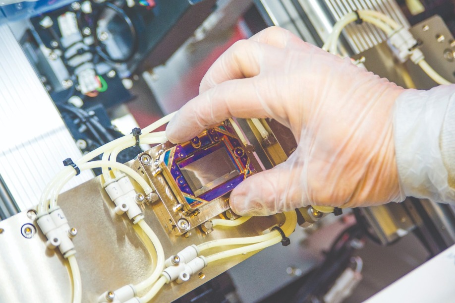
The foundry at CST Global includes an automatic bar stacker.
A: Yes. QCLs go into security and defence, and VCSELs go into industrial and consumer areas. There are well-known standard VCSEL types, but there are a lot of new wavelengths emerging. That’s not easy to do, as I’m sure you’ll appreciate. It sounds very simple to swap material and create a VCSEL at a new wavelength, but it takes a lot of re-engineering and re-qualification.
Q: What are your plans for 2019?
A: There is a hope and expectation that there will be some big opportunities this year that will take the company to a very different customer base and a very different opportunity base. I would hope that as we had last year, we will have a very significant expansion.
One promising, emerging class of applications for III-Vs is that described as quantum technologies. This rather vague moniker refers to applications exploiting quantum interference, entanglement and tunnelling. It is these
quantum phenomena that lie at the heart of atomic clocks, gravity sensors, quantum computers and quantum communications; and rely on laser cooling technology, which can be accomplished with laser diodes based on GaAs, GaN and InP.
The opportunities for quantum technologies were discussed and debated by engineers, academics, politicians, and representatives of funding agencies, at a one-day meeting held at the House for an Art Lover, Glasgow, in mid-November.
At this gathering, organised by CST Global, Sir Peter Knight from Imperial College London delivered a key note presentation entitled Quantum Technologies for a Networked World.
Knight began by highlighting the high level of investment in quantum technologies by the UK – it has allocated £400 million to a national programme. Some of those working in the UK will have also been able to draw on the €1 billion Quantum Technology Flagship, a European initiative. While these level of funding are impressive, they appear to be dwarfed by the US and China, which may be injecting as much as $2.4 billion and $10 billion, respectively.
The UK investment in quantum technology that began in 2014 is already paying dividends. It has driven the launch of the first 16 start-ups that are exploiting quantum technology; it has generated £30 million of investment; and it has created more than a hundred jobs.
Knight explained that the motivation behind such high levels of investment in the UK is in part due to improving the stability of financial markets, so that there is not a recurrence of the ‘flash crash’ – a trillion dollar crash in May, 2010, that lasted for just over half an hour. High frequency trading can contribute to panic on the markets, while the widespread deployment of atomic clocks would lead synchronisation at every node – that is, every switch, router, server, processor and GPS receiver – and ultimately greater resilience on stock exchanges.
Atomic clocks are not a new technology. This form of clock, which has a timing mechanism based on the superposition of quantum states, dates back to the 1950s. Initially, these clocks needed to operate in the lab, but applications in defence and communications have driven miniaturisation. Scaling has been spearheaded by the hugely ambitious chip-scale atomic clock programme that ran from 2002 until 2008. This effort failed to fulfill very demanding targets, but did lead to the development of a 17 cm3 chip-based clock by Symmetricom that drew less than 120 mW. Knight explained that efforts to improve on this include a design pioneered in the UK by Starthclyde and Imperial College, involving a microfabricated grating to aid laser cooling.
Another market with tremendous potential is that of quantum sensors. According to Knight, this sector includes quantum chips for accelerometry, gyroscopes, gravimetry and magnetometry, and gravity sensors for oil, gas, minerals and defence.
One of the attractions of cold-atom gravity gradiometers is that they have the potential to set a new benchmark for resolving features underground. This promises to deliver a massive boost in infrastructure productivity, which is currently held back by unknown underground conditions. Knighted illustrated this point by saying that 37 percent of delays in Dutch construction, and €70 billion in expenditure, were related to problems associated with unforeseen issues underground.
Knight concluded his talk by discussing quantum computers, which could be used to provide secure communication. Much progress has been made recently, with Intel, Google and IBM unveiling quantum computers in the last two years.
A chipmaker’s perspective on the opportunities related to quantum technologies was provide by Thomas Slight from CST Global. He explained that the accuracy of atomic clocks can be improved by progressing from those based on caesium to those that use strontium ions. The latter requires laser light sources operating at 674 nm and 422 nm. At CST, they have been developing the blue variant in projects Coolblue, and its successor, CoolBlue2, that finished this March. Efforts produced a fully monolithic, narrow wavelength 422 nm blue laser diode.
CST is also involved in three further projects related to quantum technology: an effort known as high-power phosphorous-based DFB lasers for cold atom systems, which requires a laser emitting at around 700 nm; Mac V, a collaborative effort in the UK to produce atomic clocks that use 894 nm VCSELs to probe a caesium transition; and IndICam, a programme involving the development of monolithically integrated mid-infrared imaging arrays for detecting volatile organic compounds. Another project, entitled quantum-ring single-photon LEDs, finished last June. CST’s role involved helping to produce single-photon sources based on GaSb that could be used in quantum key distribution, a technology for providing secure communication.
Successes in silicon continue to dominate the International Electron Devices Meeting (IEDM). However, in recent times this conference has also included a smattering of papers on compound semiconductor technologies.
In general, these presentations have highlighted the benefits of adding III-V epilayers to silicon. Using this approach, the likes of InGaAs have promised to extend the march of Moore’s Law, thanks to this arsenide’s superior hole mobility; and GaN has shown that it can enhance RF communication, by taking power densities to a new level.
At the latest IEDM, however, it was SiC that rose to the fore amongst the compound semiconductor technologies. At this meeting, held in San Francisco at the beginning of December, delegates discovered: how modifications to the super-junction MOSFET have enabled this wide bandgap material to set a new benchmark for on-resistance for a high-voltage SiC MOSFET; how a super-junction MOSFET formed with a multi-epitaxial growth process can produce promising switching characteristics; why SiC MOSFETs operating at 3.3 kV or more have great potential, but lack proven performance, hampering their deployment; and how sulphur doping increases the threshold voltage of the MOSFET, thereby boosting its immunity to electromagnetic interference.
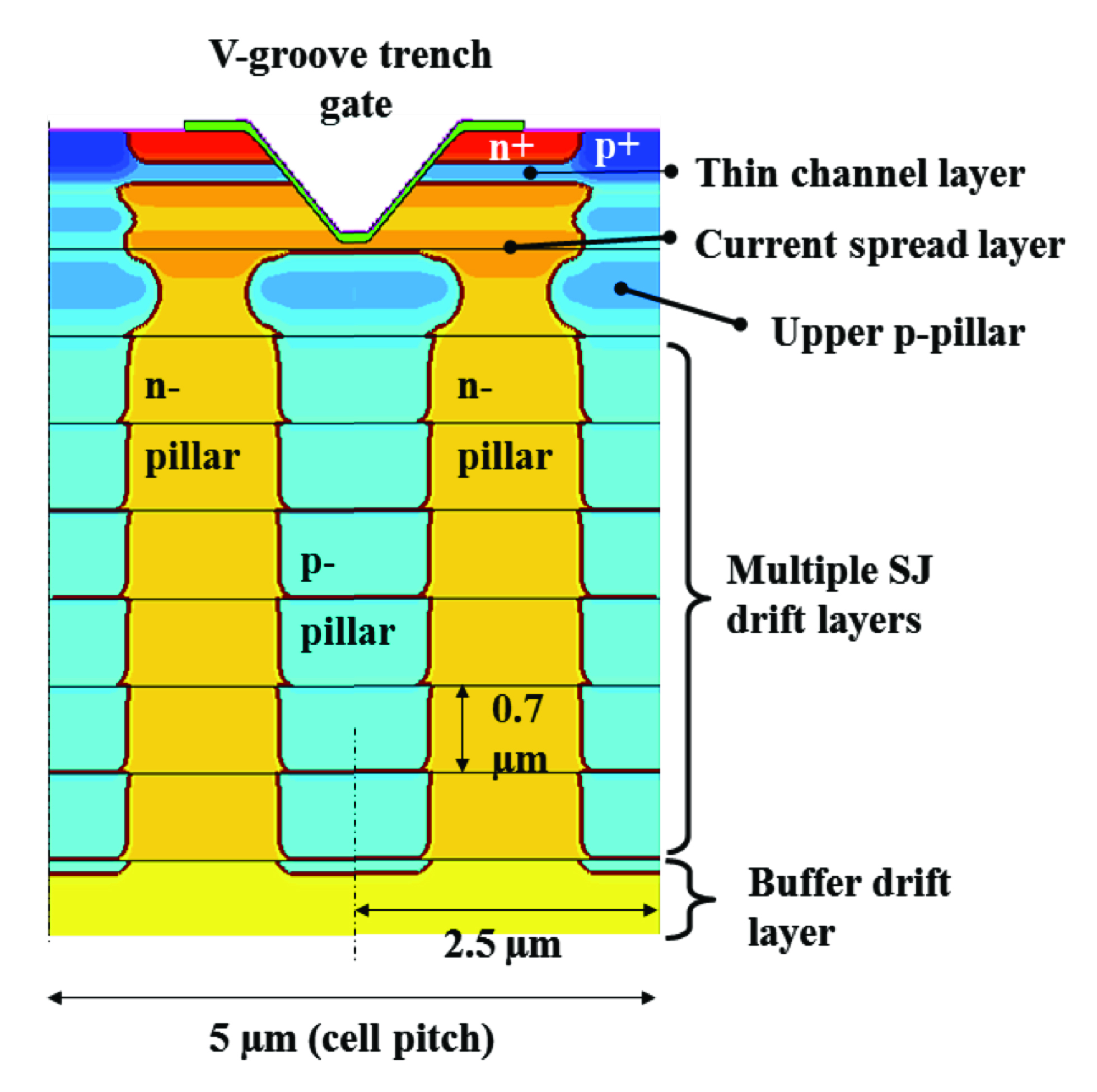
Figure 1. AIST’s SiC super-junction V-groove MOSFET is claimed to set a new benchmark for on-resistance for SiC MOSFETs with a blocking voltage in excess of 600 V. The device combines a blocking voltage of 1170 V with an on-resistance of just 0.63 mW cm2.
Super-junction success
Throughout the history of the silicon power electronics industry, innovation has been needed to propel device performance to a new level. Just before the turn of the millennium, progress came from the addition of a super-junction structure to the silicon MOSFET. This new architecture, launched independently by Siemens and STMicroelectronics, lowered the on-resistance at the drain, increased the transistor’s blocking voltage, and drove down the dynamic loss and capacitance.
Following in the footsteps of these European pioneers, engineers working for the National Institute of Advanced Industrial Science and Technology (AIST), Japan, are now increasing the performance of the SiC MOSFET via the introduction of a super-junction architecture.
At IEDM, one of the researchers at AIST, Takeyoshi Masuda, presented a paper on the characteristics of the super-junction V-groove trench MOSFET. This device combines a blocking voltage of 1170 V with an on-resistance of just 0.63 mW cm2, which is claimed to be the lowest value ever reported for a SiC MOSFET with a blocking voltage of 600 V or more.
In this novel device, the V-groove trench, aligned along the {0338} direction, reduces the channel resistance by utilizing a high-quality interface between SiO2 and SiC. Further gains mirror those found in silicon, with the super-junction structure minimising the on-resistance and breakdown voltage.
Masuda reported the first results for a SiC super-junction V-groove MOSFET back in 2016. Since then much progress has been made, with the latest results revealing dramatic improvements in the trade-off between on-resistance and blocking voltage, realised by narrowing the cell pitch of the super-junction and increasing the doping concentration in these regions.
“The cell pitch and the concentration were 7 µm and 3 x 1016 cm-3, respectively, when I presented super-junction VMOSFETs for the first time in ECSCRM 2016,” explains Masuda. In comparison, the cell pitch of the IEDM devices is just 2.5 µm, and the doping concentration 1 x 1017 cm-3.
To form the V-groove super-junction transistors, Masuda and co-workers begin by growing 3 µm-thick buffer layers that prevent a high electric field from penetrating the substrate. On this follows six cycles of the growth of n-type epitaxial layers, and then the creation of p-type regions in those layers by subsequent aluminium ion-implantation. Upper p-type pillars, doped at 1 x 1018 cm-3, are added to protect the bottom oxide of the trench from the electric field (see Figure 1).
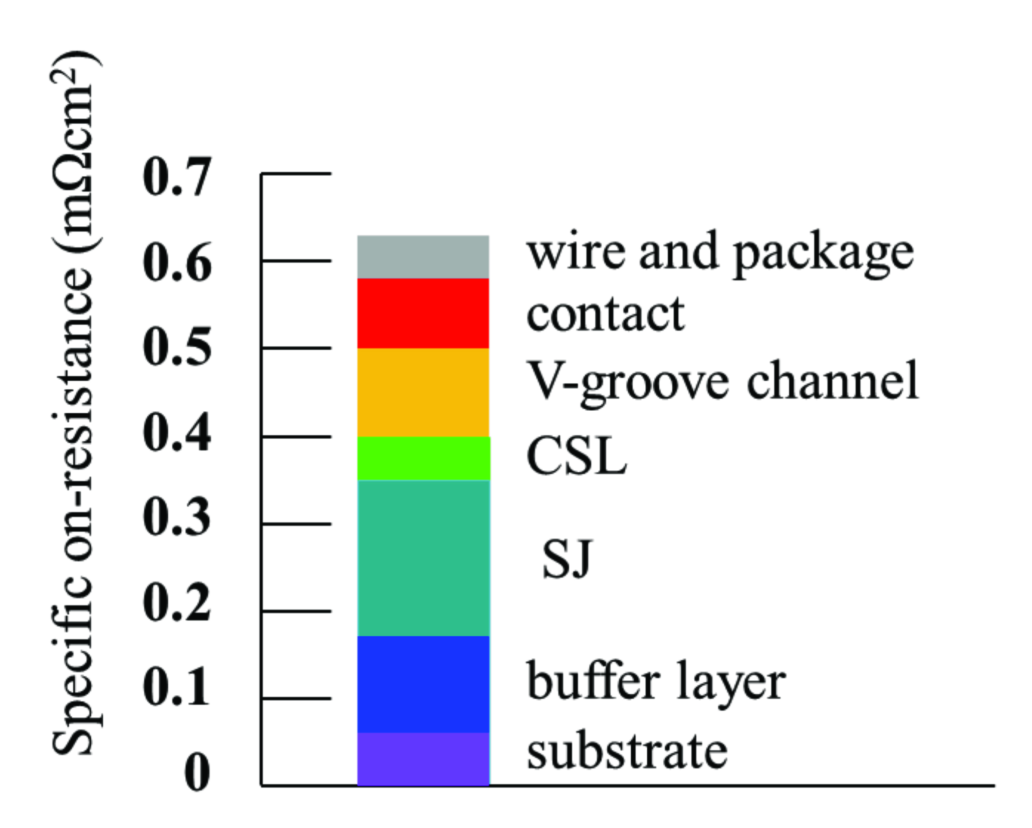
Figure 2. Analysis of AIST’s SiC super-junction V-groove MOSFET, mounted in a TO-268 package, identified the primary contributions to a total on-resistance of 0.63 mΩ cm2.
Although the six cycles of growth and implantation are not ideal, Masuda argues that this process is still suitable for high-volume manufacturing. “We demonstrated a high current density in the super junction VMOSFET. It means that the chip size can be shrunk compared with the conventional MOSFET with the same current capacity.” Yield then increases, thanks to the smaller chips.
Masuda also points out that the latest devices are prototypes. So refinements are to be expected before the process is rolled out for mass production.
Prior to the addition of the drain electrode, the 350 µm-thick substrate is ground down to just 50 µm. This step is very important, according to Masuda, as it trims resistance by more than 0.6 mW cm2.
To characterise the devices, the team mount their 0.25 cm by 0.25 cm chips, which have an active area of just 0.0377 cm2, in TO-268 packages. Using a gate-voltage of 25 V, they measured a specific on-resistance of just 0.6 mW cm2. The biggest contributor to this is the super-junction (see Figure 2).
The threshold voltage of the super-junction VMOSFET is 4.7 V, a value that is claimed to be high enough to obtain a stable off-state when being used in switching applications.
Masuda attributes this value, which is similar to that for a silicon IGBT, to the high-quality of the metal-oxide-semiconductor interface on the V-groove. “Conventional SiC MOSFETs have difficulties in achieving both a high threshold voltage and a low channel resistance because the metal-oxide-semiconductor interface quality is still poor.” He believes that there is room for further improvement in device performance, including higher blocking voltages and a lower on-resistance. “We also have to check the avalanche and short-circuit capabilities.”
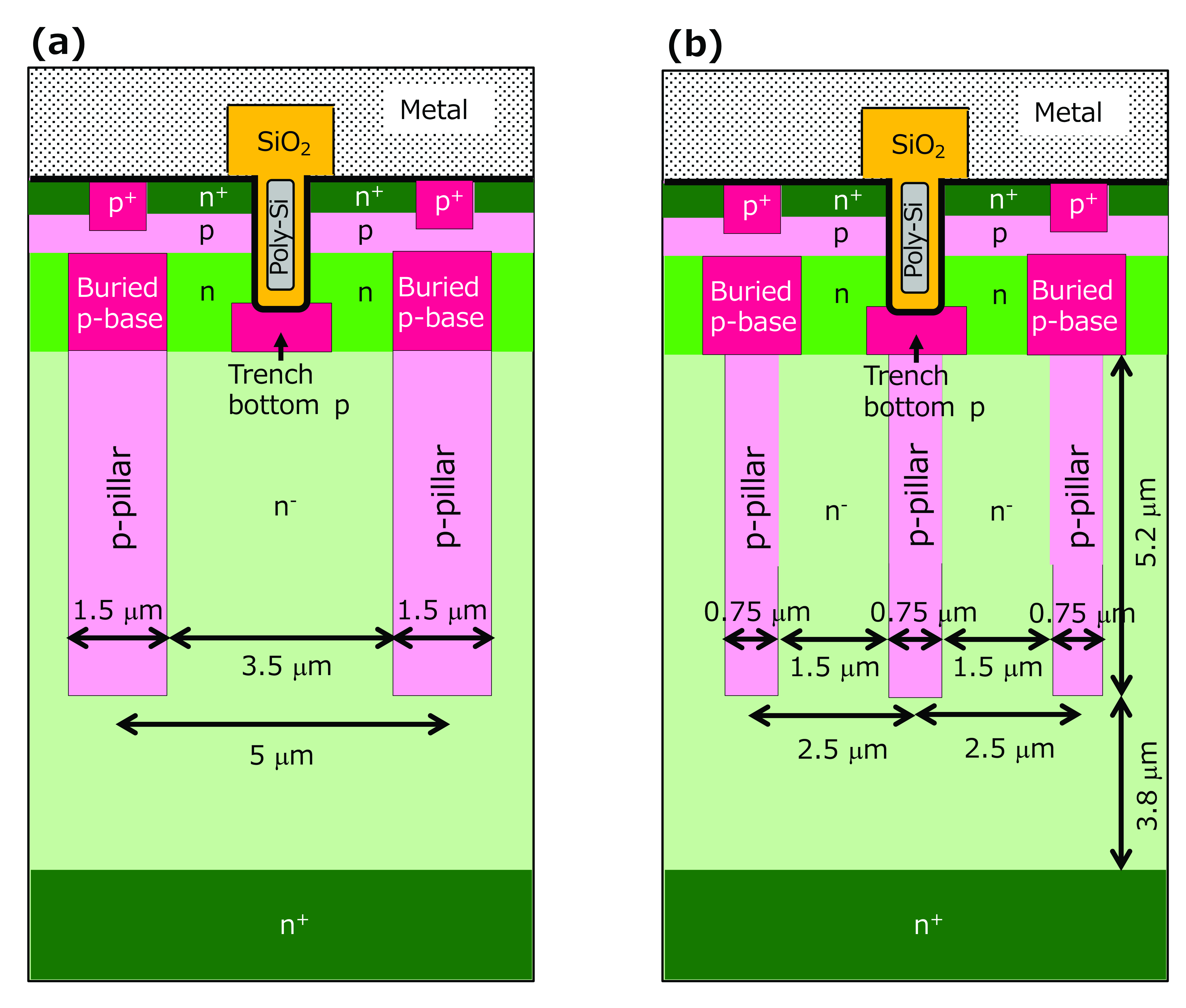
Figure 3. Engineers at AIST have produced trench-gate SiC MOSFETs with a (a) 5 µm pitch and a (b) 2.5 µm pitch.
This team began by considering two different designs. Both feature a 5 µm cell pitch and implanted buried p-base regions, which contain a trench bottom that provides a gate shielding structure. Where the designs differ is that one has 1.5 µm-wide p-type pillars connected to the buried p-type base to provide a current path, while the other employs 0.75 µm-wide pillars.
Simulations of both types of device reveal that thinner pillars reduce the specific on-resistance by
0.5 mW cm2, while thicker variants trim this figure by only 0.4 mW cm2. However, when there is a variation in the concentration of n- and p-type charges in the n-type layer by ± 10 percent, it makes more sense to make MOSFETs with the thicker pillar. That’s because when these MOSFETs are operated at 1.4 kV, there is a 0.8 µm margin in the p-pillar width for the thicker pillar, but just a 0.1 µm margin for the thinner pillar.
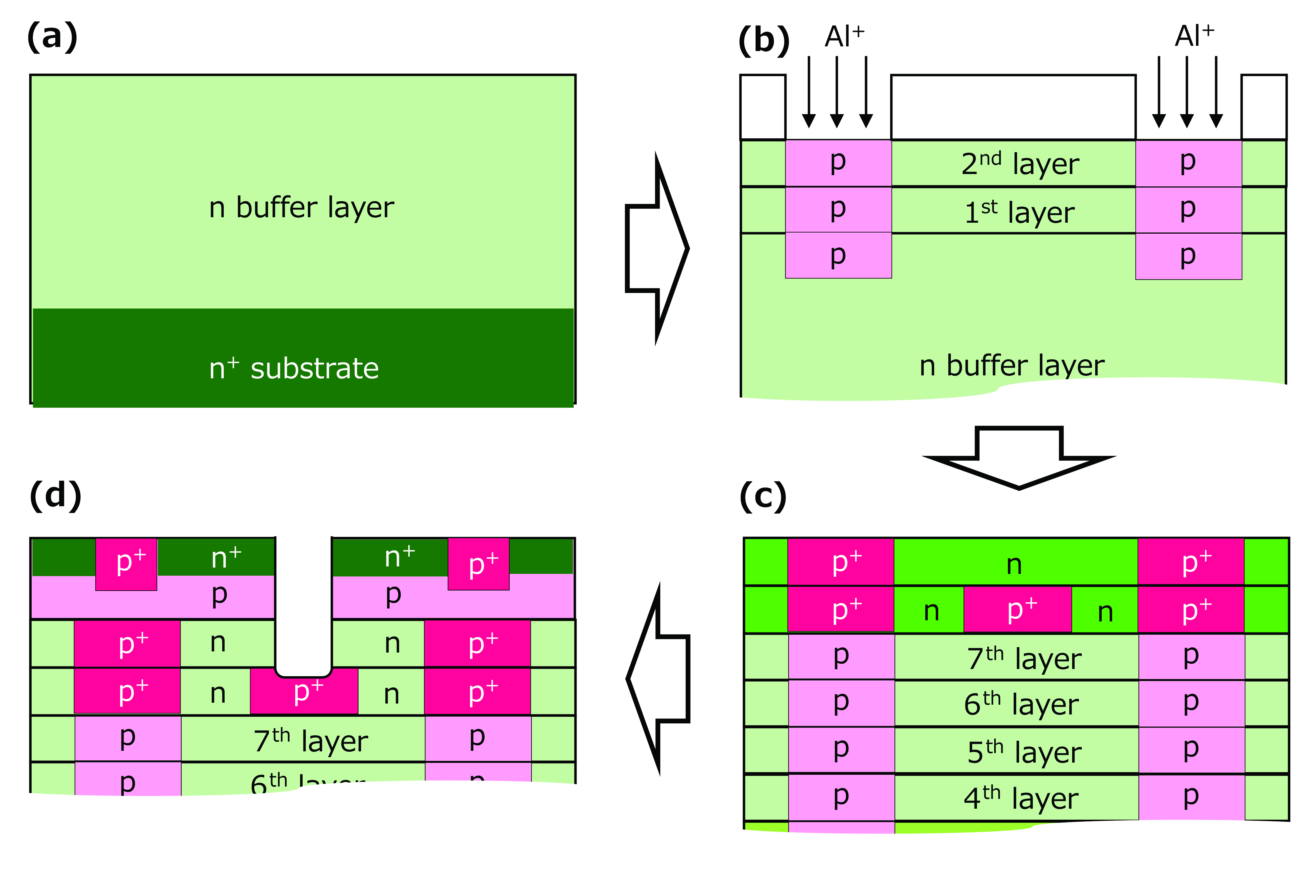
Figure 4. A multi-epitaxial growth process was used to produce AIST’s trench-gate SiC MOSFETs.
“This method is technically more suitable to form a narrow super-junction pitch than other methods, such as trench filling or high-energy implantation,” argues Harada.
Subsequent steps to producing 3 µm by 3 µm chips included forming the buried p-base regions and trench bottom p-regions through a two-step multi-epitaxial growth.
Comparing this device with a control revealed that the super-junction reduced the on-resistance from 3.1 mW cm2 to 2.7 mW cm2, while the threshold voltage remained at around 4.0 V.
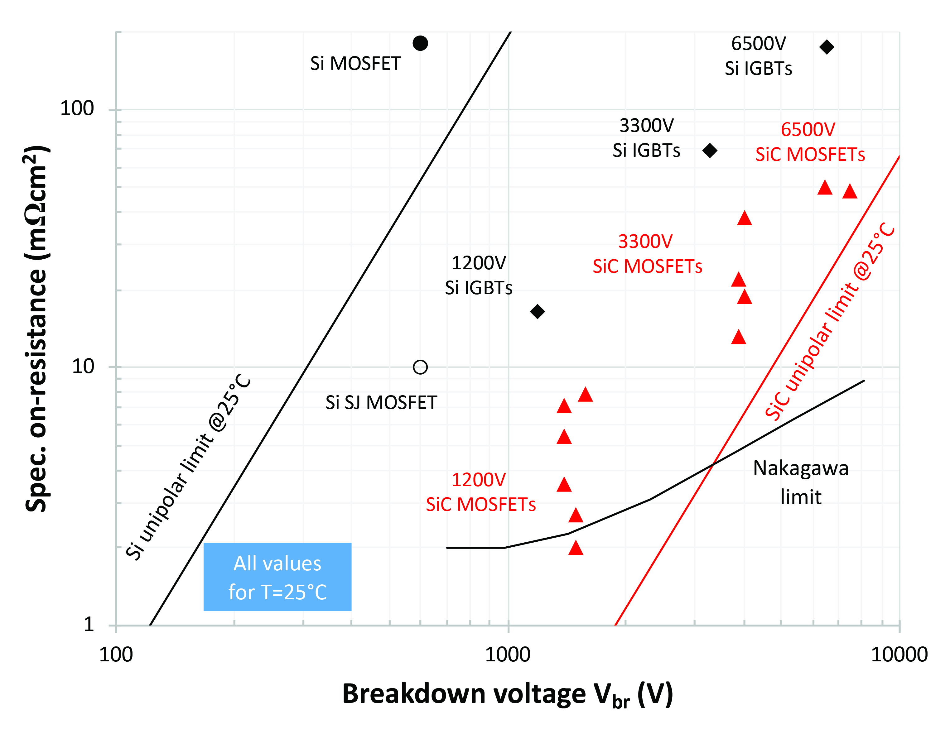
Figure 5. SiC MOSFETs with higher blocking-voltages are closer to the unipolar limit than their lower-voltage equivalents.
Measurements of dynamic performance revealed that the addition of the super-junction did not make a noticeable impact on the turn-on and turn-off switching waveforms, when a Schottky barrier diode was used as a free-wheeling diode. However, energy losses associated with turn-on were significantly higher in the super-junction device.
Short-circuit measurements, using a drain-source voltage of 600 V and a gate-source voltage of 20 V, show no degradation in the short-circuit time with the addition of the super-junction. “The obtained value is also comparable to the commercial SiC MOSFET,” says Harada.
The team is now planning to increase the blocking voltage of its devices, and improve their reliability.
3.3 kV and beyond
An evaluation of the status of high-voltage SiC, along with its prospects, was provided by Andrei Mihaila from ABB – it is a multi-national that is developing SiC MOSFET technology, but yet to release a commercial product.
According to Mihaila, SiC MOSFETs operating between 3.3 kV and 6.5 kV promise to deliver similar improvements to their lower-voltage siblings. These advantages make the devices attractive candidates for high-voltage DC and flexible AC transmission systems, high voltage drives and high-power renewable energy conversion and storage.
Encouragingly, high-voltage SiC MOSFETs are closer to the unipolar limit for this material than devices operating at lower voltages (see Figure 5). This finding led Mihaila and co-workers to conclude that static losses associated with the high-voltage SiC MOSFET predominantly stem from the doping and the thickness of the drift layer.
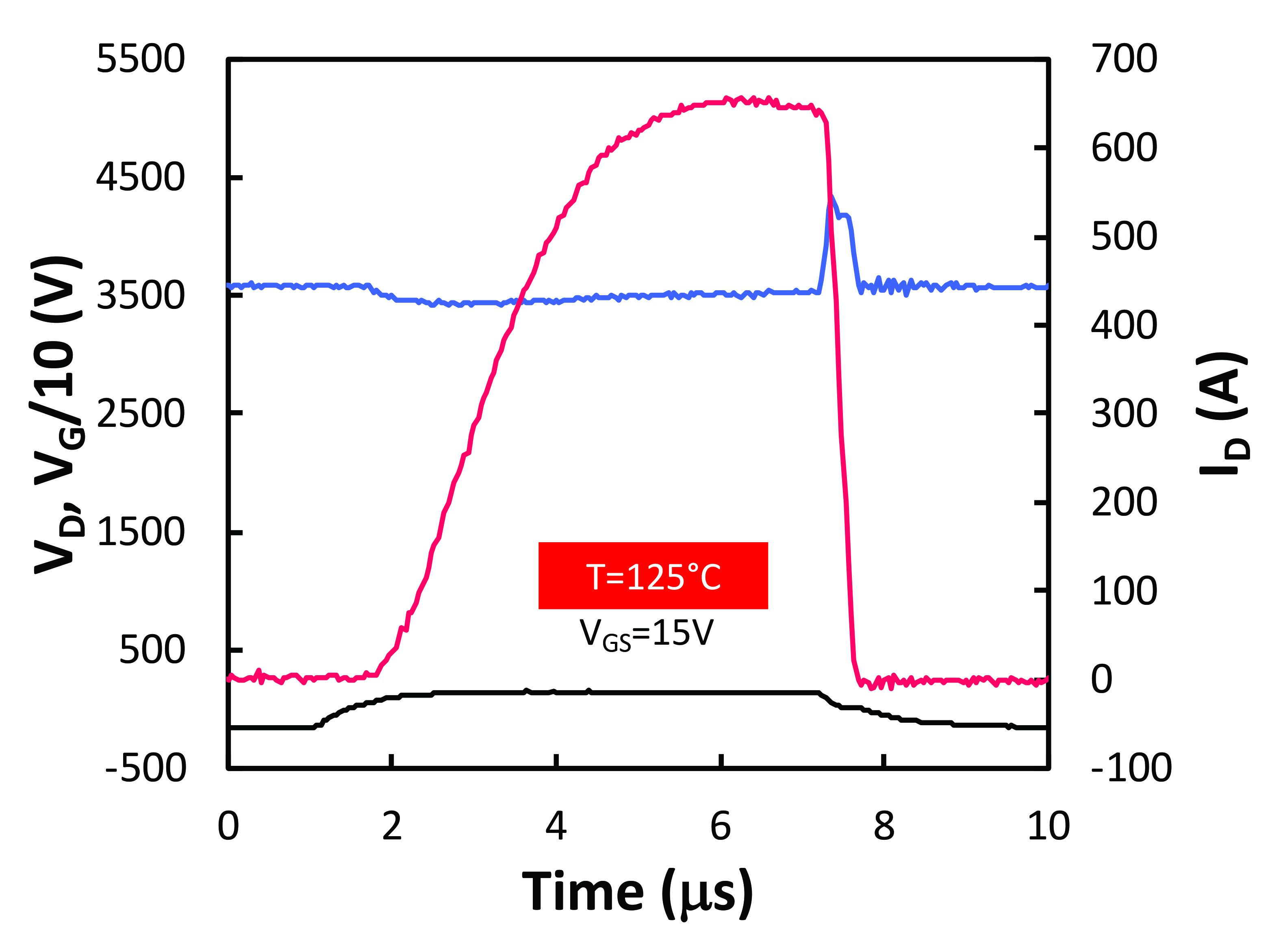
Figure 6. Engineers at ABB measured the short-circuit waveform for four 6.5 kV MOSFETs connected in parallel. Using a drain voltage of 3.6 kV, and a gate-source voltage of 15 V, the transistors exhibit a short-circuit capability of about 5 ms, with saturation current reaching levels in excess of 600 A.
He and his co-workers have compared the performance of their 3.3 kV MOSFETs with both 14 µm and 26 µm pitches with silicon IGBTs and bi-mode insulated gate transistors. Operating at 60 A cm-2, both SiC MOSFETs have lower static losses than the silicon bipolar devices.
However, the team have found that the high turn-on voltage of the MOSFET body diode leads to a higher static loss than that found in a silicon p-i-n diode. This loss, which is independent of pitch size, is attributed to the lifetimes in the epilayers.
“The body diode turn-on voltage cannot be changed,” says Mihaila, who explains that lifetime enhancing methods in the epi-layer would only alter the slope of the current-voltage curve.
The short-circuit performance of the two pitch sizes have been compared, using a drain bias of 1800 V and a gate-source voltage of 15 V. The smaller cells reduce static losses, but fail to meet the industry standard at 10 ms.
“Adjusting the cell density and the threshold voltage values towards an optimum trade-off between static loss and short circuit capability is one way of looking at these issues,” says Mihaila.
A promising approach to realising the high current levels required in high-voltage applications is to arrange several MOSFETs in parallel. Mihaila and colleagues have adopted this strategy, connecting four 6.5 kV MOSFETs in parallel. Testing reveals a short-circuit capability of around 5 ms and a saturation current topping 600 A (see Figure 6). This is claimed to be a remarkable performance for a device that is just 5 µm by 5 µm in size.
The engineers have also assessed the reverse-bias safe-operating area, finding that the 6.5 kV MOSFETs successfully turn off 80 A when using a DC link
voltage of 4.4 kV. This result, along with no failures observed during testing, led the team to conclude that this level of performance provided is similar to that provided by a state-of-the-art 6.5 kV silicon IGBT.
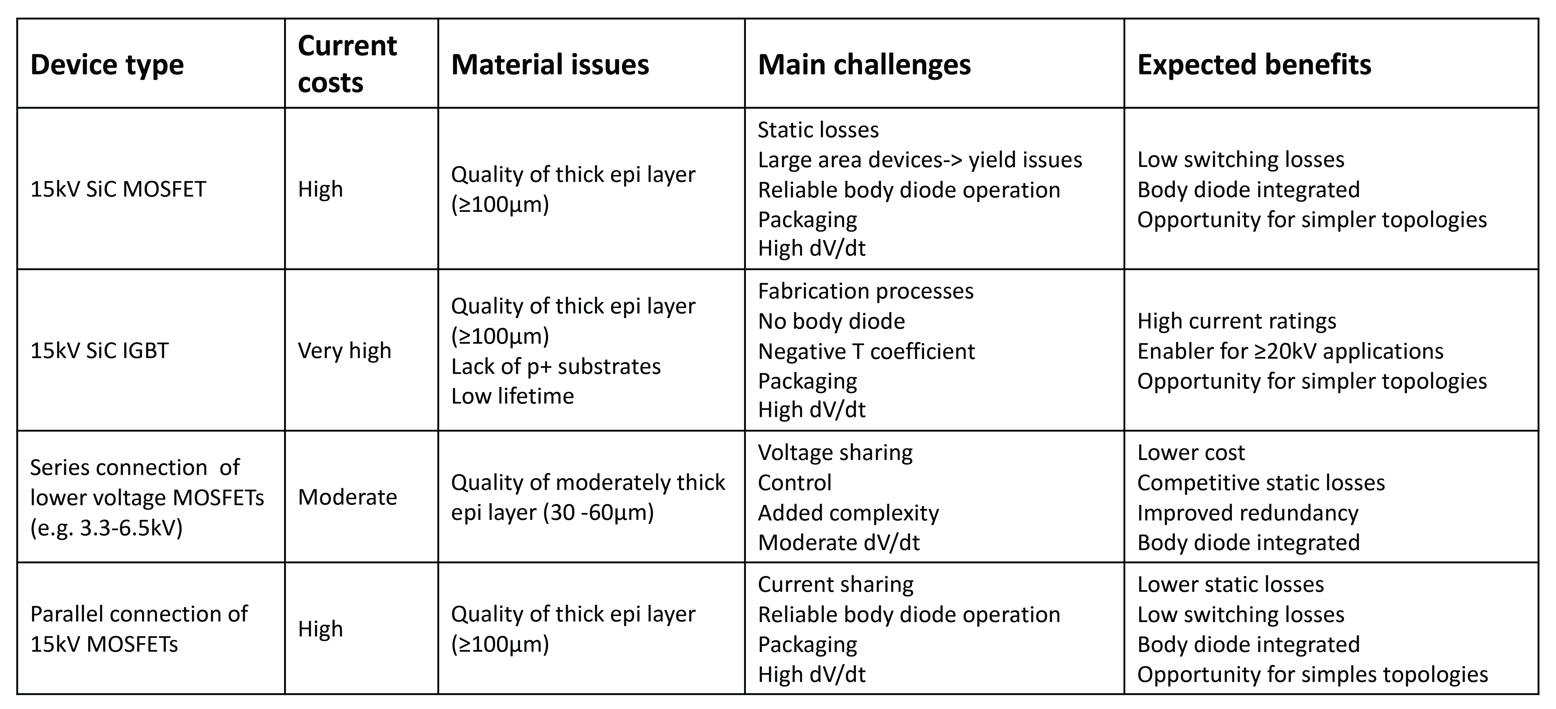
Table 1. Expected challenges and projected benefits of high-voltage (15 kV-rated) SiC devices, according to engineers at ABB.
A sulphur sweet spot
Another advance claimed at the latest IEDM concerns the first use of sulphur doping in the channel of the SiC MOSFET to improve performance.
This approach, pioneered by a team from Mitsubishi Electric and the University of Tokyo, may raise a few eyebrows, given that sulphur is known to be a deep donor that is unsuitable for device fabrication.
However, that’s only the case for bulk material – and when sulphur is used to dope the channel region, resistance can fall, trimming energy loss, while the threshold voltage increases.
Boosting the latter is a big deal, according to team spokesman, Munetaka Noguchi: “Increasing the threshold voltage of the SiC MOSFET offers superior tolerance to electromagnetic noise, which is known to cause system malfunctions.”
Noguchi and co-workers fabricated lateral and vertical silicon-face SiC MOSFETs, with sulphur doping in the channel realised by implantation. Subsequent thermal annealing activated these dopants, along with those in the source, well and p+ contact region. Addition of a 50 nm-thick gate oxide involved thermal oxidation, followed by nitridation in dilute NO.
The vertical device out-performed its lateral cousin. For this transistor, the threshold voltage is 4.0 V, and sulphur doping in the channel leads to a reduction in the resistance from 8.3 mW cm2 to 5.7 mW cm2.
According to Noguchi and co-workers, the sulphur that is in the channel can either be neutralised or ionised. If it is neutralised, the threshold voltage of the MOSFET increases, and electrons are trapped at the impurity level. And if it is ionised, it increases inversion layer mobility, thanks to a relaxation of the electric field at the metal-oxide-semiconductor interface.
Another finding by the team is that the shift in the threshold voltage resulting from a positive or negative bias stress of the gate voltage benefits from sulphur doping. This shift tends to be large for gate oxide engineering, but negligibly small for samples with sulphur doping. “Using sulphur, the threshold voltage shift is as small as that of a SiC MOSFET made with the nitridation process,” says Noguchi.
Plans for this team include further development of SiC power devices that are tolerant to electromagnetic noise. If they succeed, and the engineers of AIST and ABB do with their SiC devices, these teams may report the details at next year’s IEDM. But more comprehensive coverage of breakthroughs in SiC is sure to be provided at the International Conference on Silicon Carbide and Related Materials (ISCRM), which will be held this autumn in Kyoto, Japan.
Gallium-oxide trench-type power devices with novel architectures have the attributes to trump those made from silicon carbide
BY KOHEI SASAKI AND AKITO KURAMATA FROM NOVEL CRYSTAL TECHNOLOGY AND SHIGENOBU YAMAKOSHI FROM NOVEL CRYSTAL TECHNOLOGY AND TAMURA CORPORATION
The days of the internal combustion engine are numbered. Concerns over climate change are encouraging governments to consider banning sales of petrol and diesel vehicles by 2030 or so. And even in those countries that many not enact this legislation, there will be many individuals living there that will be turning to electric vehicles to do their bit for the environment.
Even before the ban, sales of electric cars will climb as they fall in price and deliver an ever better performance, including being able to go further on a single charge. This will be accomplished in part by increasing the efficiency associated with the power system that drives the car. Today, significant losses occur in the semiconducting power devices used to alter the current or frequency of electricity, due to considerable electrical resistance of the components. Trim these losses and the range of the car could increase, tempting drivers to make the switch to a zero-emission vehicle.
The incumbent material for power semiconductors is silicon. Replacing this with the leading alternative, SiC, cuts losses. However, devices made from this wide bandgap material have non-negligible manufacturing costs, and it is difficult to use them in non-industrial applications, such as home electronics and private vehicles.
A far more promising option is the ultra-wide bandgap material gallium oxide, which has a huge critical electric field strength (see “The strengths of gallium oxide” for details of its great material properties). In the form of its β-polytype, it has been used to make incredibly low-loss devices with breakdown voltages of over 600 V. The hope is that one day device fabrication costs will be as low as they are for silicon, because β-Ga2O3 wafers can be made with a melt growth method that is similar to the one used to make silicon wafers. Due to these positive attributes, β-Ga2O3 power devices have great potential for deployment in electric vehicles – there are even plans to start installing them in this class of car by 2025.
The cost of chip production is governed by economies of scale. Larger epiwafers are needed to drive down costs, and our team from Novel Crystal Technology and Tamura Corporation are working towards this. Currently, we are selling 2-inch b-Ga2O3 epitaxial wafers (see Figure 1), and this market is taking off, with sales of this material doubling annually. But as well as building new growth chambers to meet demand, we are also producing larger versions to meet requests for larger wafers. Later this year, we will also start to sell 4-inch β-Ga2O3 epiwafer samples.
In addition, we are preparing for the manufacture of a portfolio of high-performance devices. Read on to learn about the development of our ground-breaking diodes and transistors.
Trench diodes
Special device structures may be needed to explore the full potential of β-Ga2O3. That’s certainly the case with the Schottky barrier diode. Adopt a conventional design and device characteristics are limited by the leakage current at the Schottky junction.
We overcome this limitation with a periodic trench metal-oxide-semiconductor (MOS) structure (see Figure 2). Inserting this trench under the anode electrode decreases the electric field at the Schottky junction, leading to a reduction in the leakage current.
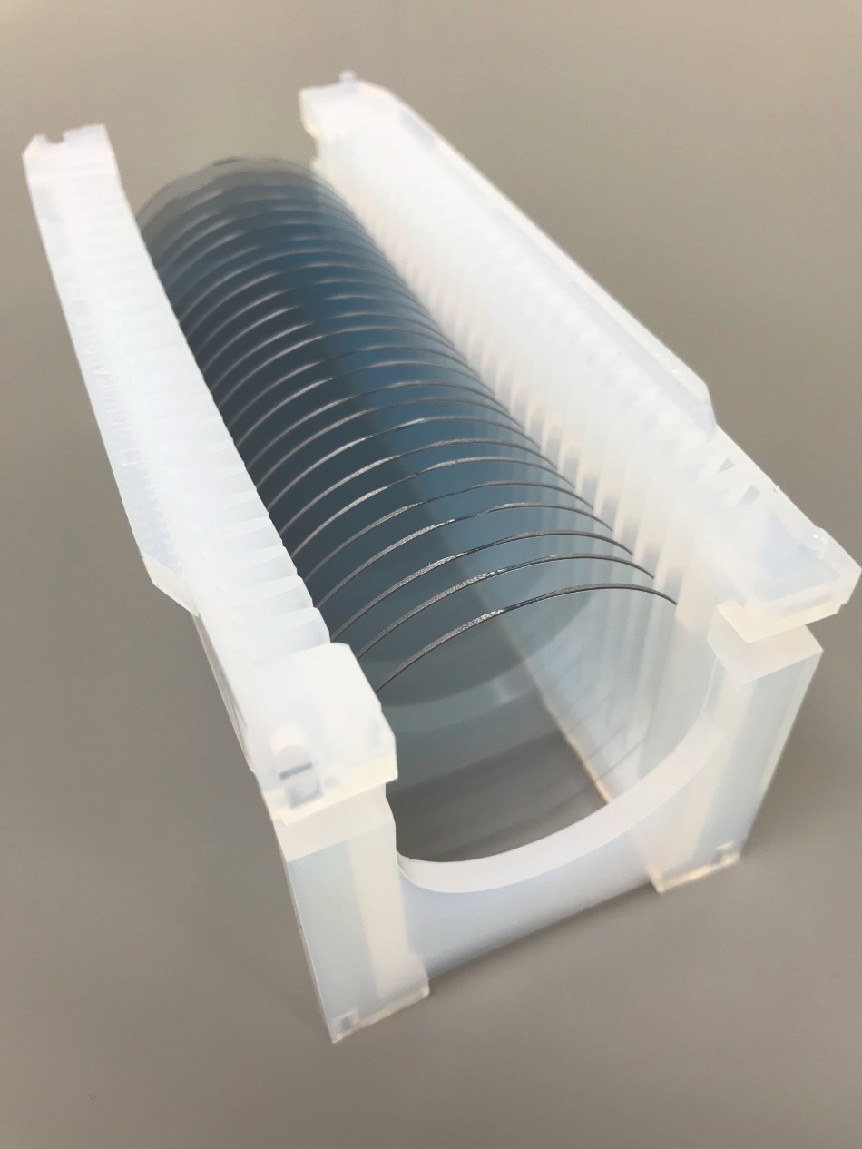
Figure 1. 2-inch single crystal b-Ga2O3 wafers produced by Novel Crystal Technology.
Reverse bias measurements of our MOS Schottky barrier diode reveal that it has a leakage current comparable to that of commercially available SiC Schottky barrier diodes (see Figure 3(a)). The breakdown voltage of our device is only 400 V, because we are still developing our anode edge termination technique. Higher voltages will result from the introduction of guard rings, along with other modifications.
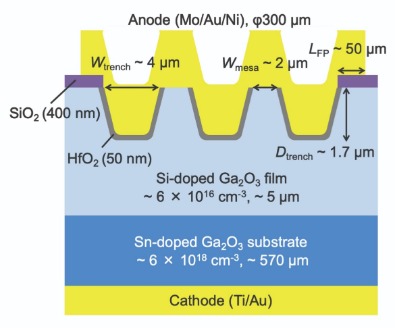
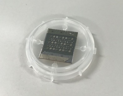
Figure 2. The β-Ga2O3 trench metal-oxide-semiconductor Schottky barrier diode developed by Novel Crystal Technology and Tamura Corporation.
We are confident that when our β-Ga2O3 MOS Schottky barrier diodes are used to replace silicon p-n diodes in power factor correction circuits, boosting choppers and inverters, they will cut the power loss of the system. We are currently developing a device fabrication technique for mass production. Manufacture of a limited numbers of test samples commenced last year, and full-scale production is planned for 2021.
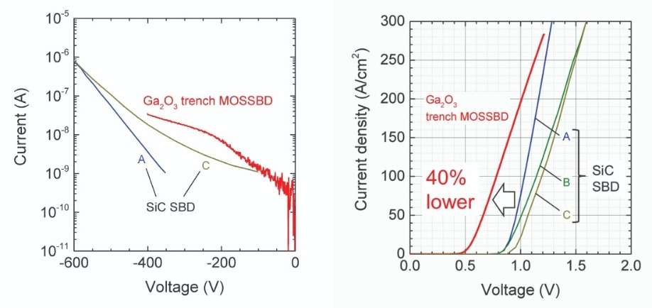
Figure 3. (a) Reverse and (b) forward characteristics of a b-Ga2O3 trench metal-oxide-semiconductor Schottky barrier diode and a commercially available SiC Schottky barrier diode. The b-Ga2O3 device exhibits about a 40 percent lower forward loss than that of the SiC Schottky barrier diode, and has small reverse-leakage characteristics.
Junction barriers
Another option for decreasing the leakage current at the Schottky junction is to embed the p-type region under the anode electrode. This creates a device known as a junction-barrier-controlled Schottky diode, which has similar characteristics to the trench MOS structure that we have just described.
Making this device is not easy, because p-type doping techniques are not available for β-Ga2O3. Our solution is to use a heterojunction, pairing p-NiO with n-Ga2O3.
To ensure success, we had to determine the electrical characteristics of the junction between these two oxides. Knowledge of the breakdown voltage would be crucial to developing a high-performance device. To this end, we fabricated a simple p-n diode by growing an n-Ga2O3 film on a Ga2O3 substrate, before adding p-NiO by RF sputtering. The resulting heterojunction has a high breakdown voltage – it is over 700 V – and good forward characteristics. These are very promising results, given that this p-n junction contains an amorphous film.
Armed with what we have learned, we fabricated β-Ga2O3 junction-barrier-controlled Schottky diodes (see Figure 4 for details of their design). Trenches were formed by dry etching, and filled with p-NiO. To complete fabrication, molybdenum Schottky electrodes and titanium ohmic electrodes were added.
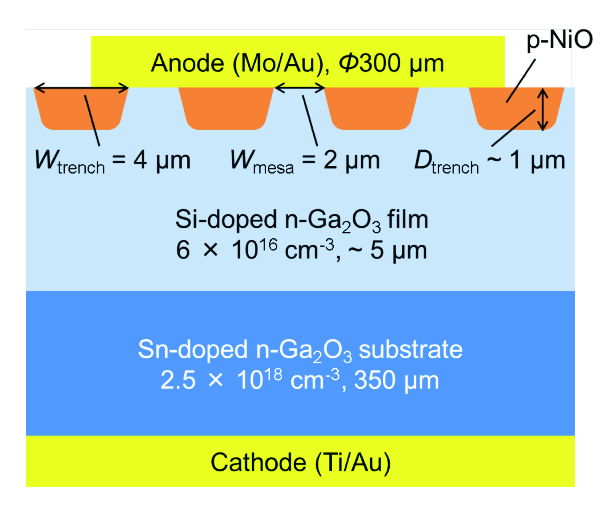
Figure 4. Schematic illustration of b-Ga2O3 trench junction-barrier-controlled Schottky diodes.
When it comes to forward characteristics, the p-n diode is inferior to both the junction-barrier-controlled Schottky diode and the Schottky barrier diode. The latter two have a threshold voltage of 0.5-0.6 V, compared with 2.2 V for the p-n diode (see Figure 5). These results indicate that the forward current of the junction-barrier-controlled Schottky diode flows through the Schottky junction normally.
Even better results should be possible by using the p-NiO/n-Ga2O3 heterojunction to make guard rings that prevent the electric field from concentrating too much at the electrode. These structures are essential for realizing high-breakdown-voltage devices.
Based on the result so far, and the potential for further improvement to the junction-barrier-controlled Schottky diode, we believe that this device has a great future. Its major asset is that it compensates for a major weakness in β-Ga2O3 – the absence of a p-type doping technology. Development is proceeding smoothly, and we are considering mass production.
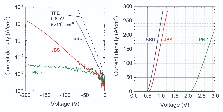
Figure 5. (a) Reverse and (b) forward characteristics of junction-barrier-controlled Schottky diodes (JBS), Schottky barrier diodes (SBD), and a diode with a p-n junction (PND). The black dotted line indicates the calculated thermionic emission current for a normal Schottky barriers diode.
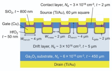
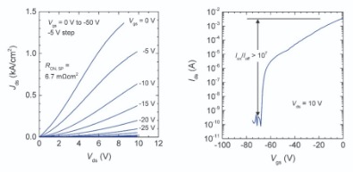
Figure 6. (a) Schematic illustration, (b) current density-voltage, and (c) transfer characteristics of a β-Ga2O3 trench MOSFET.
Power transistors
Our next target is the development of β-Ga2O3 power transistors. Due to the lack of p-type doping, we are working with a static induction transistor-type structure, made from entirely n-type material. A hallmark of this device is that its behaviour can be adjusted from a normally on FET to an off variant by simply changing either the mesa width or the donor concentration in the mesa region.
We have developed a normally on device (see Figure 6 for the device design). This is easier to make than its normally off sibling, simplifying our efforts to demonstrate operation of vertical β-Ga2O3 FETs. We fabricated this transistor using the process developed for trench MOS Schottky barrier diodes.
Measurements on this device reveal a huge current density – it is over 1.3 kA/cm2 – and clear current modulation upon application of a gate voltage (see Figure 6(b)). Transfer characteristics show that the on-off ratio is over 107
Further reading
K. Sasaki et al. IEEE Electron Device Lett. 38 783 (2017)
K. Sasaki et al. ICSCRM 2017, WE.E1.7
K. Sasaki et al. Appl. Phys. Express 10 124201 (2017)
(a) Z. Hu et al. IEEE Electron Device Lett. 39 869 (2018)
The potential of β-Ga2O3 is highlighted by its value for Baliga’s figure of merit, which is a guide to how suitable a material is for power devices. The figure for β-Ga2O3, calculated from its material properties, is 3,000 times larger than that of silicon and ten times that of SiC.
Behind this high figure for β-Ga2O3 is its extremely large bandgap – it is about 4.5-4.8 eV. This figure offers an estimate of the critical electric field strength of 8 MV/cm (see table below).

To make devices, there is a need to dope material. The doping concentration in β-Ga2O3 can be controlled over the range 1015-1020 cm-3 by impurity doping, in spite of the large bandgap.
The great potential for β-Ga2O3 power devices is underscored in the plot above. The theoretical limit for the specific on-resistance, illustrated by the solid line, is 3,000 times smaller than that of silicon devices and one-tenth that of SiC devices for the same breakdown voltage.
Another merit of β-Ga2O3 is that large single-crystal substrates can be produced with the melt-growth method. As this growth technology is already used for the manufacture of silicon and GaAs substrates,
it is expected that large, high-quality β-Ga2O3 substrates can be easily manufactured at low cost.
Theoretical specific on-resistance as a function of breakdown voltage. The solid lines indicate the theoretical limit, determined from the material properties.
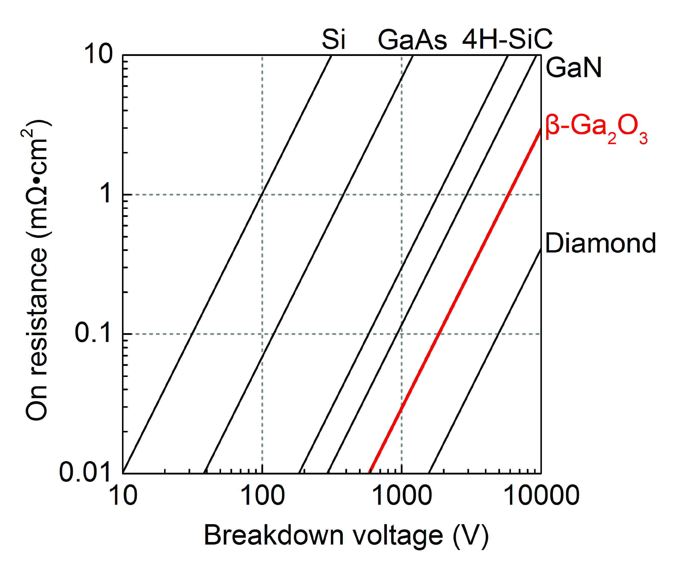
Screening the substrate, optimising a fast growth process and going slow in the cool-down step are three ingredients to high-yield, high-volume production of SiC epiwafers
BY NICOLÒ PILUSO FROM STMICROELECTRONICS
SiC has many great attributes, making it a very promising material for numerous applications. Its low intrinsic carrier concentration and high thermal conductivity make it a strong candidate in the automotive sector; its combination of a low thermal expansion coefficient, high hardness and tremendous linearity in harsh environments give it great potential in uses related to astronomy; and its high band gap, high drift velocity and high breakdown voltage are enabling it to succeed in the power electronics market.
To ensure that SiC can excel in all these sectors, there is a need for high-yield manufacturing of devices with a high crystal quality. That means that the SiC epilayers that are grown on the substrate, usually 4H-SiC, must combine a high degree of uniformity across the wafer with a low defect density, as well as thicknesses and doping concentrations that hit their target values.
Our team at the STMicroelectronics R&D Group and Production Group in Catania, Italy, can excel on all these fronts, due to our expertise in developing SiC growth processes for high-volume, high-yield production of high-performance power devices.
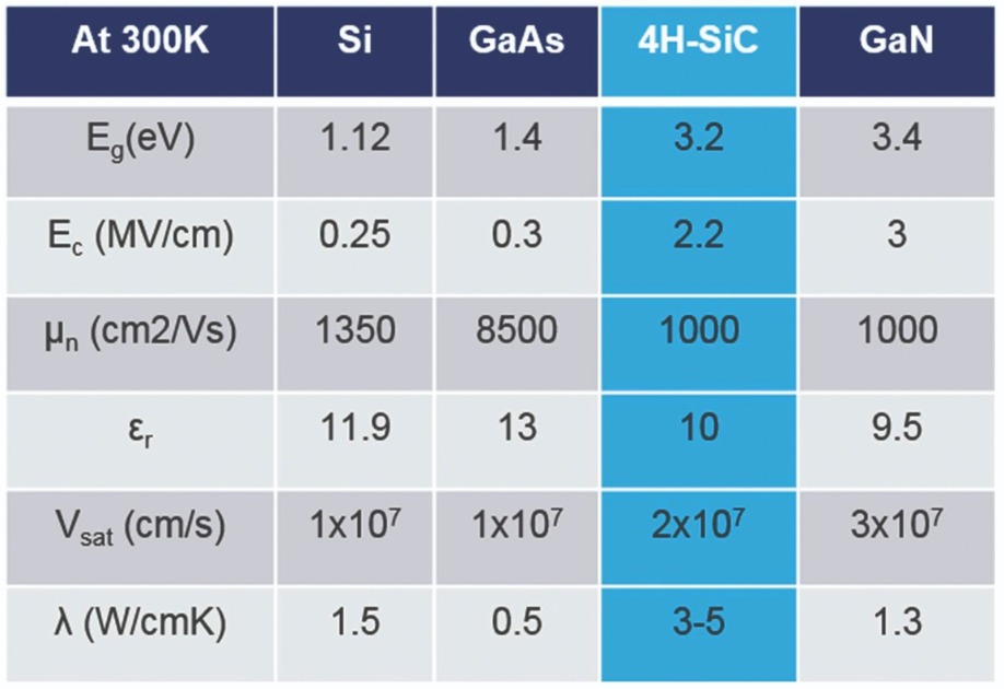
Table 1. SiC has a great set of attributes.
Heating the wall
The most common reactor for the growth of 4H-SiC homoepitaxial layers is the Hot Wall CVD (HWCVD) reactor. Its primary advantages over cold wall designs are its low thermal gradient, the long lifetime of the susceptor and the low back-deposition. For high-volume manufacture, horizontal reactors with a rotating holder are preferred, because they drive down production costs.
SiC epilayers are formed by introducing silicon and carbon precursors into a chamber containing substrates heated to around 1600 °C. The precursors are decomposed and atoms of silicon and carbon impinge on the substrates, migrate and bind together to form SiC epilayers (see Figure 1, which highlights the main chemical reactions occur during the epitaxial growth, as well as the design of the HWCVD tool).

Figure 1. (left) Decomposition of precursors on the substrate surface, followed by migration of atoms, leads to 4H-SiC homoepitaxy growth. (right) Growth of SiC epiwafers is most commonly undertaken in a horizontal hot-wall CVD reactor.
Eradicating defects
Many different classes of defect can plague SiC epilayers (see Figure 2 for an overview). These imperfections arise from either a local instability in temperature or pressure, a non-optimal balance of silicon and carbon precursors, or a slow growth rate. To ensure good material quality, it is also imperative to grow the epilayers on a high-quality substrate.
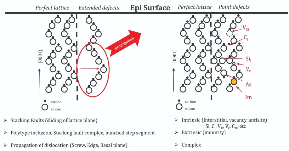
Figure 2. The defects that occur during 4H-SiC homoepitaxy can be sub-divided into extended and point defects.
Other forms of extended defect include polytype inclusions, and dislocations that propagate. The inclusion of 3C and 6H polytypes, which can occur during the epi-growth, may change local, fundamental parameters of the host semiconductor, such as the band edge, thermal conductivity and carrier lifetime. This leads to drastically degraded electrical characteristics. Dislocations can also be disastrous, shortening the local carrier lifetime – and in cases where pits propagate, accelerating deterioration of the oxide. One imperfection of this form is the carrot defect, which is predominantly generated by a threading screw dislocation propagating in the substrate. There are also triangles, an extended defect that originates from the presence of particles or carbon inclusions on the surface during growth.
As well as all these forms of extended defect, there are point defects. They act as trap centres, and when they are found in MOSFETs, they impair channel mobility, decrease carrier lifetime and cause a hike in the reverse-bias current.
There is no quick fix to addressing all these imperfections. What’s needed is a comprehensive, careful study of what the potential pitfalls are at every step of the epitaxial process, and how they can be avoided. Such a study must consider the impact of time, precursor ratios, temperature, pressure, and gas carriers, not only on the growth steps, but also on the loading and unloading of the wafers (as illustrated in Figure 3).
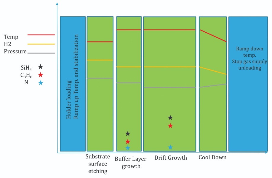
Figure 3. The growth of SiC devices by CVD involves surface etching, the growth of buffer and drift layers, and a cool down step.
We have devoted much effort to trimming the etching time below 10 minutes, in order to cut the defect density and increase doping uniformity. The decline in thickness uniformity can be kept in check by raising the temperature, because this bolsters the effectiveness of surface etching.
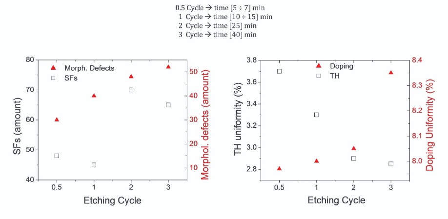
Figure 4. (Left) The number of defects as a function of etching time. (Right) Thickness and doping uniformity as a function of etching time.
Once the surface is clean, we begin to grow the epitaxial structure, starting from buffer layer, using nitrogen and aluminium as the n-type and p-type dopants, respectively. The substrate is typically highly doped – the level usually exceeds 1018 atoms/cm3 – so to minimise the doping gap between this and the device layers, the buffer is doped, typically at a concentration between 1015 atoms/cm3 and 1017 atoms/cm3. Additional roles for this layer are to quash the conversion and propagation of substrate defects, known as dislocations, into the epilayer.
An appropriate level of doping must be combined with sufficient epilayer thickness. That’s because thicker layers reduce extended defects, which have a very strong, detrimental effect on device performance (see Figure 5). Unfortunately, this thick layer must be grown slowly during buffer layer growth to prevent the propagation of a kind of dislocation called a basal plane.
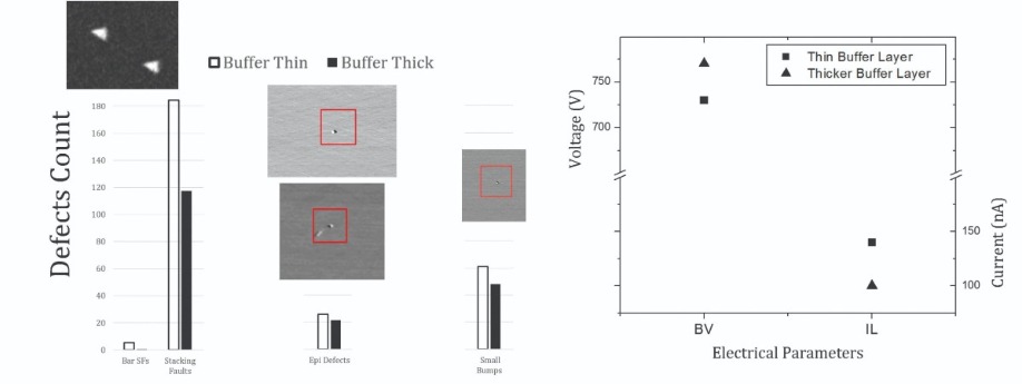
Figure 5. Thicker buffers reduce the defect densities in the epilayer (left), and improve the performance of the MOSFET (right), which benefits from a higher breakdown voltage and a reduction in leakage current.
Our latest efforts are directed at studying the impact of the nitrogen flux on the buffer layer. Descending doping ramps during buffer layer growth appear to reduce lattice stress introduced by nitrogen, enabling the growth of a compliant drift layer.
... and the drift layer
It is well known that as epitaxial defects rise, electrical characteristics are compromised. However, to guarantee the functionality of the devices, when it comes to the drift layer, it is essential to combine a very low defect density with high uniformity in thickness and doping. In fact, there are many requirements for the drift layer – in addition to withstanding a high voltage (together with the gate oxide), it has to host many critical manufacturing processes, including post-oxidation annealing, gate oxide fabrication, ion implantation, and thermal annealing.
During the last decade, we have devoted much effort to improving the crystal quality of our epitaxial process. Success has followed and now 95 percent of the area on 6-inch epiwafers is useable, based on calculations using a 2 mm by 2 mm grid. The key to this progress has been the fine tuning of: the growth temperature, which should be uniform within the chamber and higher than 1600 °C; the growth pressure, which should be stable and lower than 100 mbar; and the carbon-to-silicon ratio, which should be within the range 1.1 to 1.3.
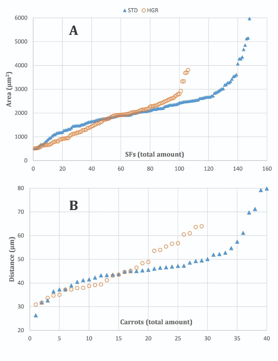
Figure 6. Moving from a standard growth rate process (STD) to a high growth rate process (HGR) reduces stacking faults (A) and carrots (B) in the epilayers.
Many groups have shown that increasing the growth rate, in tandem with the use of substrates off-cut by 4°, enables a trimming of defect density and improvement in thickness and doping uniformity. By appropriately balancing silicon and carbon precursors and the silicon-to-hydrogen ratio (H2 gas and argon are the typical gas carriers), growth can hit 20 μm/h.
In our laboratories, we have observed these trends, with a strong reduction of defectiveness at higher growth rates. This includes reductions to the density and the size of crystallographic defects, such as stacking faults, and the morphological defect known as a carrot (see figure 6).
To negate the influence of substrate quality on our results, we used material with a very similar crystallographic quality – all substrates came from a small section of one ingot. By taking this precaution, we are confident that it is the higher growth rate that leads to a 10 percent hike in electrical yield, thanks to a reduction of defect density and improvements in thickness and doping uniformity. Evaluating the latter with a figure of merit that equals the difference between the maximum and minimum values, divided by the mean, gives values of less than 5 percent for thickness and below 12 percent for doping.
Cooling down
After growth of our epilayers, our wafers cool down, the gas supply is stopped and the gas line purged. The rate of the cooling is important, as it governs the thermal stress induced within the epilayers. If the stress is significant, it can generate post-growth defects. The hydrogen flow is also a consideration, as this determines the generation of shallow defects, just a few nanometres in size.
We have found that by slowing the cooling rate to less than 25 °C/min, and increasing the flow of hydrogen, we can reduce the thermal stress and increase the time that the surface of the epiwafer is at a higher temperature.
Our approach, which we refer to as a ‘high growth rate cool’, is beneficial. It reduces, by 40 percent, both the number of small defects, defined as having a size of less than 1 μm, and the number of shallow defects, which are just a few nanometres in size. Another feature of our cooling process, which provides an effective cleaning of the surface, is to increase the pressure a little bit.
The combination of the higher growth rate and the slower cool down decreases the density of all major defects (see Figure 7). Thus is encouraging, but our work is not over, as we still need to undertake a
careful inspection of the relationship between epilayer quality and the major growth parameters, including pressure, growth rate, the temperature ramp and the carbon-to-silicon ratio. It is clearly very important to optimise the growth process for every single layer and the cool down. However, this, in itself, cannot guarantee epiwafer quality. That’s because it is also necessary to screen the quality of the substrates, which are formed by slicing ingots and polishing the resulting material.
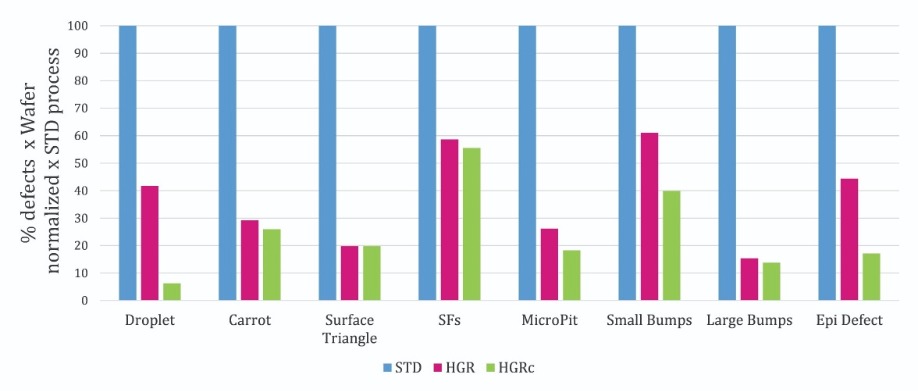
Figure 7. Epilayer crystal quality, judged in terms of defects density, improves by advancing from a standard growth rate process (STD) to a high growth rate process (HGR) that includes a superior cool down (HGRc). Note that the percentage has been normalized to that for the STD process.
We have carried out a statistical survey, evaluating defect densities in thousands of wafers before and after the epitaxial process. This study revealed that when substrates come from an ingot with a nominal dislocation density of less than 3000 per cm2, epilayers have a low defect density even when they are taken close to the seed of the ingot, which is the worst part of the boule. However, if the dislocation density is higher, there is a faster deterioration of epitaxial layer quality, especially for substrates close to the seed (see Figure 8).
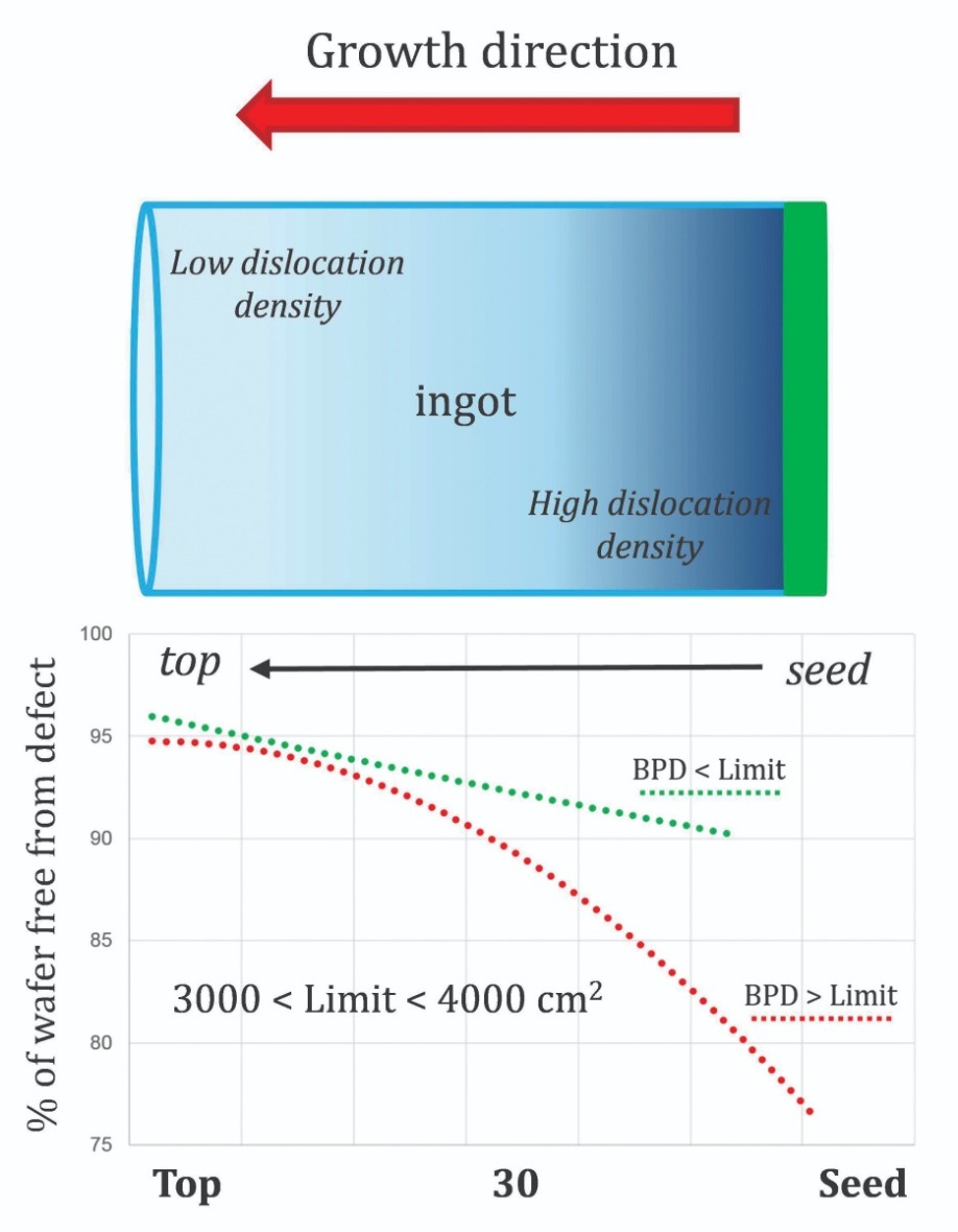
Figure 8. Using wafers with a basal plane dislocation density of less than 3000 per cm2 leads to a significant improvement in epiwafer quality.
Further reading
Y.M. Tairov et al. J. Cryst. Growth 43 209 (1978)
N. Kuroda et al. Extended Abstracts, 19th Conference on Solid State Devices and Materials, Tokyo, Japan, 1987, p. 227 Step controlled VPE growth of SiC single crystals at low temperatures
A. Itoh et al. Silicon Carbide and Related Materials 1993, IOP, p. 59, (1994).
D.J. Larkin et al. Appl. Phys. Lett. 65 1659 (1994)
O. Kordina et al. Silicon Carbide and Related Materials 1993, IOP, p. 41, (1994)
N.Piluso et al. Mater. Science Forum 897 181 (2017)
N.Piluso et al. MRS Advances 1 3673-3678 (2016)
T. Kimoto Jap. J. Appl. Phys 54 040103 (2015)
T. Kimoto et al.. Fundamentals of Silicon Carbide Technology, ISBN: 978-1-118-31352-7 (2014)
F. La Via, Silicon Carbide Epitaxy, ISBN: 978-81-308-0500-9 (2012)
Equipping silicon with InGaAs channels improves the logic and high-frequency performance of RF-CMOS
BY CEZAR ZOTA, CLARISSA CONVERTINO AND LUKAS CZORNOMAZ FROM IBM ZURICH
The digital revolution defines our times. We live in the information age, enabled by a huge flow of data – it passes through submarine communication cables, is encoded on high-frequency electromagnetic waves, and flows in and out of computers, which process it with the help of billions of transistors. Today, we not only take it for granted that we have immediate access to information and social networks, but also to continual improvement in all these technologies. We expect smartphones, laptops and personal computers to get faster and more efficient, and to have connectivity at higher rates.
For many years, the development of computers and gadgets kept pace with the shrinking of silicon CMOS technology, via the scaling laws of Robert Dennard. Those rules established a way to miniaturize the silicon transistor, while improving its performance and maintaining chip power density. This has been accomplished by a simultaneous reduction of the supply voltage and key transistor dimensions, such as the gate oxide thickness and the gate length.
Dennard scaling had a good run, starting in the 1960s and continuing all the way to the beginning of this century. But in the end, the physical limits of electron transport have caught up with scaling, through two key phenomena that only hold back highly scaled, modern transistors.
The first of these is that a reduction of the supply voltage, perhaps paradoxically, leads to an increase in the off-current when the on-current is maintained at a constant level, in order to avoid degradation of the processor clock rate. In practice, the supply voltage cannot drop below 0.7 V, which is today’s value in state-of-the-art silicon CMOS finFETs.
The second phenomenon is a trimming of the increase of the on-current with gate-length scaling, due to the device entering the so-called ‘quasi-ballistic regime’ – a carrier transport mode where electrons don’t scatter as they travel through the transistor channel.
Both of these effects have had a profound impact on scaling. This no longer produces an increase in processor clock rate, which has hovered at around 3 GHz for more than a decade. Instead, since 2003, reductions in transistor dimensions have held the key to a higher transistor density and enabled the introduction of multi-core processor architectures.
Another impact of the disabling of the traditional scaling paradigm has been the heralding of an era of developments driven by innovation and material science. Recently, the roll-out of a new technology node has hinged on reductions in dimensions and the introduction of novel device concepts and materials. They have included high-k dielectrics, strained silicon and SiGe, and finFET device architectures.
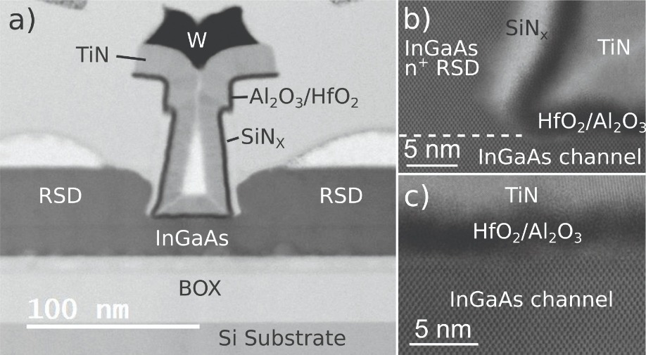
Figure 1. (a) Cross-sectional transmission electron microscopy of a fabricated RF-MOSFET. Close-up on (b) the contact side, showing the raised contact epitaxy as well as the SiN spacers, which reduce parasitic capacitances by separating the contacts from the gate, and (c) the channel region and the gate oxide interface, showing nearly pristine crystal quality of the III-V.
III-V credentials
In this era, there has been much interest in compound semiconductor materials. Their high electron mobilities promise to improve the nFET channel in CMOS technology and boost the drive current in future nodes. For example, InGaAs has an electron mobility six times that of bulk silicon, and could allow a reduction in supply voltage to 0.5 V. That’s a big deal, as it would halve power consumption.
Applications where compound semiconductors are already making a lasting impact include high-frequency technologies, such as radar and wireless communication. Improvements in HEMTs and HBTs have played an important role in the evolution of wireless technology from the fully analogue 1G format of the 1980s to today’s 4G networks. And III-Vs will be an essential ingredient in the roll-out of 5G, which promises peak data rates of 10 Gbit/s and vastly increased network capacity.
The engineers that have developed high-frequency transistor technology have followed different rules from those that advanced silicon CMOS. For starters, scaling is far less critical. Another key difference is that this device employs a semiconductor gate barrier, rather than an oxide. This modification results in a far higher electron mobility. However, this is at the expense of a reduction in electrostatic efficiency, due to the combination of a relatively small dielectric constant and an increase of the gate leakage, stemming from the much smaller band gap of the barrier. The upshot is limited scalability. Progress has instead been driven by device structure optimization, alongside a reduction in parasitic capacitances and resistances, and in particular gate resistance.
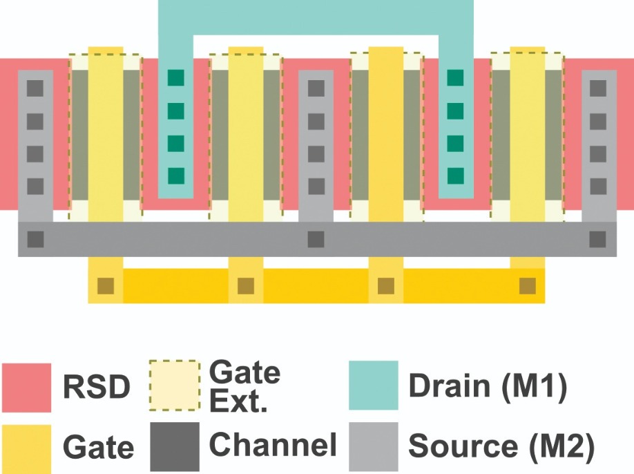
Figure 2. The layout of IBM’s RF-MOSFET with four gate fingers. The gate extension layer indicates an additional metal line on top of the gate metal to reduce the gate resistance.
There are two reasons for this, both associated with the semiconductor gate barrier. Firstly, due to insufficient electrostatic control, gate-length scaling is inefficient. Secondly, it is not possible to scale down the gate barrier thickness. Doing this increases gate leakage, so increasing oxide capacitance is not possible. This limits the peak transconductance, which directly influences ft and fmax.
The solution to both these issues is to replace the semiconductor gate barrier with a high-k gate oxide. For the last ten years, much effort has been devoted to this, focusing on the demonstration of high-frequency III-V MOSFETs. To date, they lag HEMTs by about a factor two in ft and fmax, primarily due to reduced mobility that arises from electron scattering off of defects in the gate oxide. Nevertheless, the MOSFET outperforms the HEMT in transconductance, due to improved scalability. In particular, MOSFETs from MIT show great promise, reaching 3.45 mS/μm. The potential of these devices could be unlocked with their implementation in a high-frequency compatible architecture.
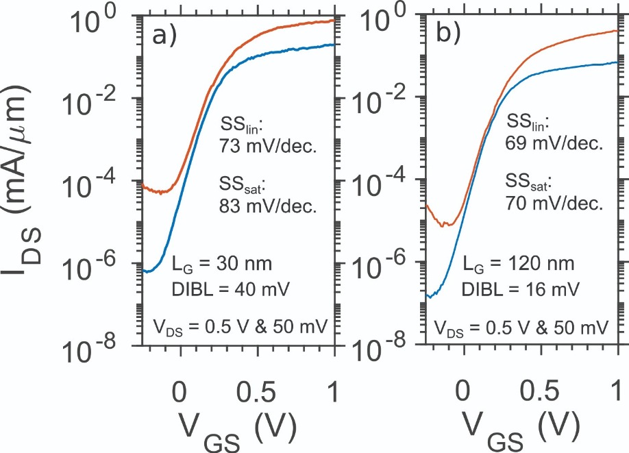
Figure 3. Subthreshold characteristics for short and long-channel finFETs for logic applications. The tri-gate architecture of the finFET improves electrostatic control to reduce the off-current at the intended bias point.
Higher frequencies
The concept of a high-frequency MOSFET is certainly not novel. Within the silicon CMOS industry, there is a class of technology called RF-CMOS. The basic premise is the tweaking of state-of-the-art silicon CMOS technology nodes, so that devices can serve both high-frequency and logic applications.
This dual functionality has many merits. It is lower in cost than III-V HEMT technology, which requires III-V substrates and expensive crystal growth methods. What’s more, by combining RF and logic, this technology allows for tight integration of the likes of wireless communication functionality and digital signal processing. Thanks to this, there can be reductions in delays and form factors, much valued by today’s mobile industry.
However, silicon technology is still held back by the inferior mobility of this material. For example, Intel’s 22 nm RF-CMOS fiFET low-power technologies are limited to 230 GHz and 284 GHz for ft and fmax, respectively.
Given this limitation, it is attractive to integrate III-Vs with RF CMOS technology. While the hike in drive current offered by InGaAs at length scales of 5 nm CMOS and below might not fully compensate for the cost of integrating the III-V channel, the large boost in RF performance could tip the scale in III-V’s favour.
It is not easy to unite III-Vs with RF CMOS. The challenges include how to make high-performance III-V transistors with a silicon CMOS-compatible process flow that is as close as possible to standard fabrication technology, and the key issue of how to integrate III-V channels on silicon substrates. In addition, there is the need to co-optimize logic and high-frequency devices in one technology.
At IBM Research Zurich we have broken new ground by recently succeeding in this endeavour. Our approach involves integrating InGaAs channels on silicon via direct wafer bonding. We cap both a target silicon wafer and a source III-V wafer, which contains the channels, with a bonding oxide that provides adhesion. Both wafers are brought together, and annealing and subsequent stripping of the source wafer leaves a thin III-V layer on an oxide layer on silicon.
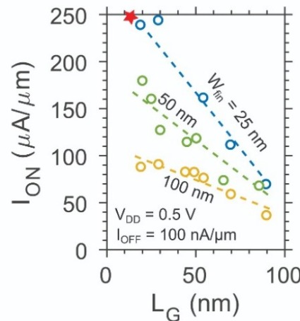
Figure 4. Comparison of the on-current, defined at a specific supply bias and off-current, for various gate lengths. The red star indicates IBM’s previous results at IEDM 2017, for a solely logic-suitable technology. With IBM’s latest technology, a similar logic performance is realised while also implementing high-frequency functionality.
There is still room for improvement, as the bonding defect density needs to be reduced to ensure the high mobility of the III-V layers. However, there is no doubt that direct wafer bonding has matured into a technology facing imminent industrial use.
One of the strengths of our III-V RF-CMOS technology is that it employs a fully silicon CMOS compatible process flow. Processing includes a gate-first high-k/metal gate flow, producing self-aligned source and drain regions that are raised and in situ doped, as well as a palette of silicon-compatible materials. By taking this approach, we highlight the possibility of a cost-effective introduction of III-Vs in a silicon technology. Added foundry costs are minimal.
We have used our process technology to make finFETs with 20 nm-wide InGaAs fins. Benchmarking performance against III-V-on-silicon at a competitively scaled gate length – including a comparison with
our platform just targeting logic, reported at IEDM 2017 – reveals that our latest transistors are on a
par with the state-of-the-art. This evaluation is based on a drive current of 250 mA/μm, realised for a fixed off-current and a supply voltage of 0.5 V.
Our latest chip also features RF-MOSFETs. Simultaneous delivery of impressive high-frequency and logic performance results from SiN source and drain spacers that trim the overlap capacitance to the gate electrode, and source and drain contact extensions underneath the spacers. Note that simply adding spacers to reduce parasitic capacitance and thus improve high-frequency performance is not good enough, as this also degrades logic performance by introducing large access resistors in the ungated parts of the channel under the spacers. We avoid this with a novel approach that involves a controllable etch of a small cavity under the spacers, followed by a refilling with a low-resistive contact material that reduces the impact of access resistors.
Armed with this architecture, our InGaAs RF-MOSFETs are capable of an ft of 400 GHz – this is the highest value reported so far for a III-V RF-MOSFET. Following optimisation of our device layout, we obtain a balanced performance of 215 GHz for ft and 300 GHz for fmax. These values are close to the performance of silicon RF-CMOS from Intel and GlobalFoundries.
Higher frequencies are possible. Capacitances are still limiting high-frequency performance, and improvements could be realised with thicker spacers and longer contact extensions. Another refinement is the introduction of a thin quantum well in the channel. This will lead to a hike in mobility, by reducing scattering at both the gate and back oxide interfaces. Making these changes should propel our technology from matching the performance of state-of-the-art silicon equivalents to outperforming them by a considerable margin – and ultimately making a strong case for the integration of III-Vs and silicon.

Table 1. A benchmark for various III-V-on-silicon technologies as well as state-of-the-art silicon RF-CMOS. Comparing the high-frequency performance, our new work shows III-Vs for the first time matching silicon RF-CMOS.
Further reading
H. Hahn et al. IEDM Tech. Dig. 17.5.1-17.5.4 (2017)
B. Sell et al. IEDM Tech. Dig. 685 (2017)
C. Zota et al. VLSI Techn. Symp. T15-5 (2018)

GaN VCSELs with long cavities and curved mirrors combine very low threshold currents with high production yields
Engineers for Sony are claiming to have set a new benchmark for the threshold current of the GaN-based VCSEL. At the International Workshop on Nitrides (IWN), held in Kanazawa, Japan, last November, project leader Tatsushi Hamaguchi revealed that the threshold current for its blue-emitting laser can be as low as 0.25 mA.
This record-breaking result, which aids wall-plug efficiency that hits 9.5 percent, is realised with a novel VCSEL design that combines a curved bottom with a cavity length that is far longer than usual – it is tens of microns in length.
Adopting this architecture, and developing the processes used to fabricate it, address two of the biggest challenges associated with conventional GaN VCSELs: how to produce the bottom mirror, and how to ensure lateral optical confinement.
Sony’s efforts will help to spur the deployment of GaN-based blue and green VCSELs in various applications, including optical storage, laser printers, projectors, displays and solid-state lighting.
Green variants may also serve in optical communication, by emitting in a spectral range with a low absorption coefficient in plastic optical fibre.
The idea of equipping a VCSEL with a curved mirror came to Hamaguchi during a late night in the lab. His design has similarities with the vertical-external-cavity, surface-emitting-laser, although that tends to operate as an optically pumped device.
With Sony’s VCSEL, the curved mirror is formed on the backside of the substrate, leading to a cavity that is far longer than that of conventional designs. That’s a massive benefit, as it makes it far easier to ensure that the thickness of the cavity is well-matched to the reflectivity of the mirror. Note that with a conventional design, the length of the cavity is typically well below ‘10l’, so its thickness must be controlled to within far less than 1 percent of a target value to enable lasing to occur at a wavelength within 5 nm of the preffered value.
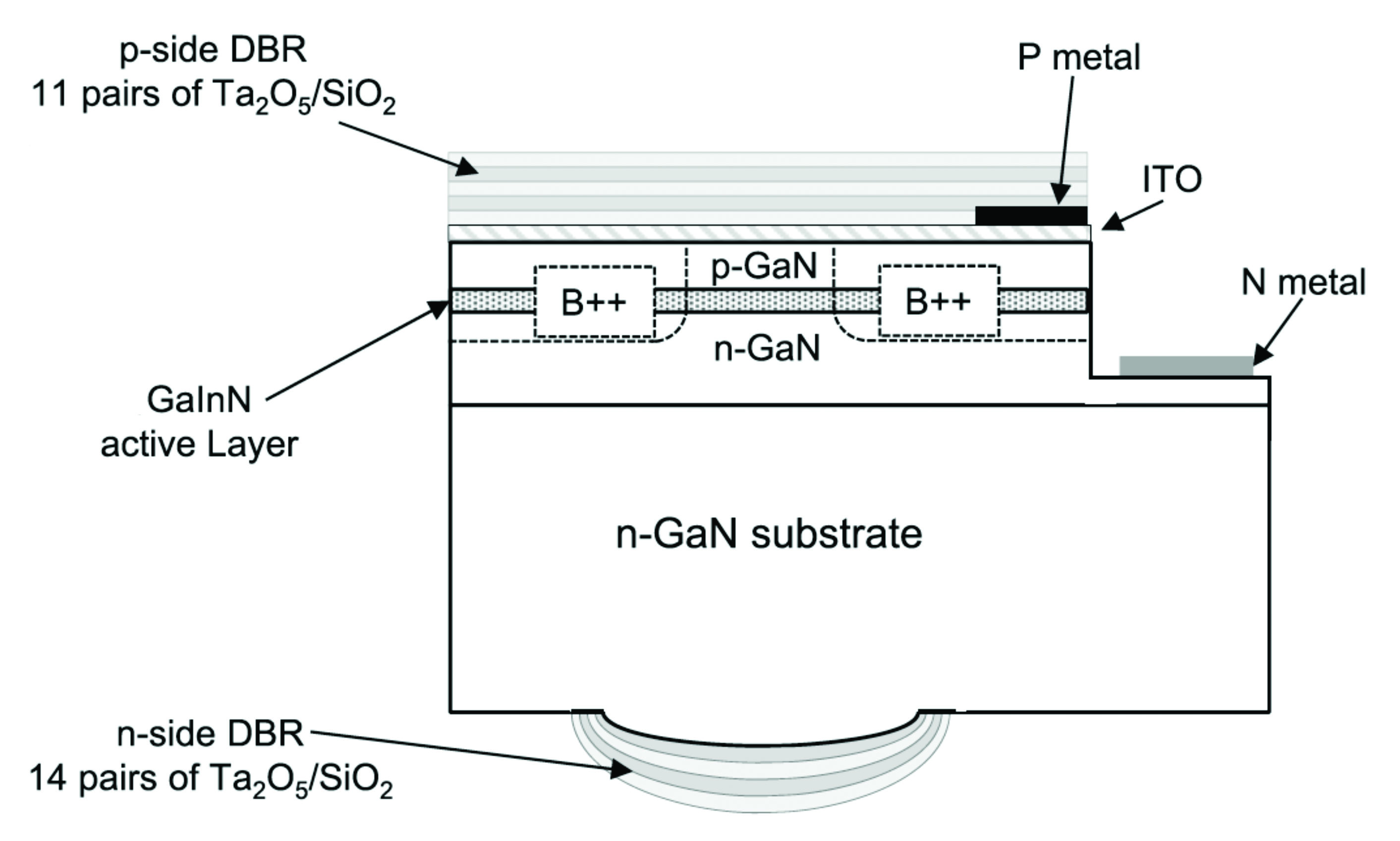
Caption: Sony’s curved mirror creates a VCSEL that forms a stable cavity that is from free diffraction and scattering loss.
To produce the curved mirrors on the lapped surface, the engineers add resin discs to this side of the epiwafer, using photolithography to define
dimensions. Heating the discs to 200 °C melts them into droplets, which provided sacrificial masks for a reactive ion etch that creates lens-shaped protrusions in the wafer.
Adding an n-type DBR to this side of the wafer, and metal and ITO electrodes for current injection, completes device fabrication.
Scrutinizing the flatness of the curved mirror with atomic force microscopy reveals a root-mean-square surface roughness of far less than 1 nm, a value comparable to that for plane mirrors used in VCSELs. Atomic steps are seen in the maps.
Measurements show that the team’s VCSEL with a 3 mm aperture produces a maximum output power of 0.3 mW at 5 mA. This laser has a front mirror reflectivity of more than 99.9 percent, and a threshold current of just 0.25 mA.
Increasing the cavity to 8 mm and reducing the front-mirror reflectivity to 99.3 percent results in an increase in output power to 12 mW at 25 mA along with a hike in threshold current – it shoots up to 3.8 mA. Wall plug efficiency hits 9.5 percent at 20mA.
Hamaguchi told the delegates at IWN that the team’s approach offers “good reproducibility and yield”. Lasing yield is 100 percent, and the threshold is stable, with a scattering of ±10 percent.

MOCVD-grown hexagonal BGaN heterostructures underscore the potential of this layered, wide bandgap material system
Engineers at Texas Tech University are claiming to have produced the first nitride-based semiconductor alloy system with a layered structure. Using MOCVD, the team have deposited boron-rich BGaN alloys and quantum wells on a hexagonal BN epilayer.
Hexagonal boron nitride is in fact the only wide bandgap semiconductor with a structure that is layered – all its peers form three-dimensional structures.
Layered structures have great potential, thanks to their tremendous characteristics. They have an extremely large exciton binding energy, a high in-plane carrier mobility, a high absorption and emission efficiency, and an extremely high breakdown field.
BGaN-based devices with tuneable optoelectronic properties could result from the efforts at Texas Tech.
“Heterostructure and quantum well devices, including detectors, emitters and transistors, can potentially benefit from this new alloy system,” argues team spokesman Hongxing Jiang.
In his view, the devices with the most promise are those that either operate in the deep ultraviolet, emit single photons or detect neutrons.
Jiang and his co-workers produce their samples by loading sapphire substrates into an MOCVD reactor equipped with triethylboron, ammonia and trimethylgallium precursors – these sources provide the boron, nitrogen and gallium content, respectively.
To support the crystallisation of BGaN alloys into the hexagonal lattice, the team first deposits a 10 nm-thick hexagonal BN layer at around 1350 °C. The engineers then add a range of BGaN layers of similar thickness, after dropping the temperature to 1225 °C to aid incorporation of gallium.
X-ray diffraction reveals that the quality of these layers is inferior to that of the underlying hexagonal BN. However, peaks overlap, indicating that the alloys have crystallised into a nearly hexagonal lattice.
The position of the X-ray diffraction peaks have been used to determine the lattice constants for BGaN at various flow rates. This suggests that as the flow rate starts to increase, so does the lattice constant. However, for flows of 4 cubic centimetres per minute or more, the lattice constant is fixed. X-ray photoelectron spectroscopy indicates that the samples with high flow rates contain B0.93Ga0.07N.
Jiang and co-workers think that a miscibility gap, similar to that found in InGaN, might explain why only a limited proportion of gallium atoms can be incorporated into BGaN.
To investigate the conductivity of their alloys, the team constructed metal-semiconductor-metal structures with interdigitated fingers.
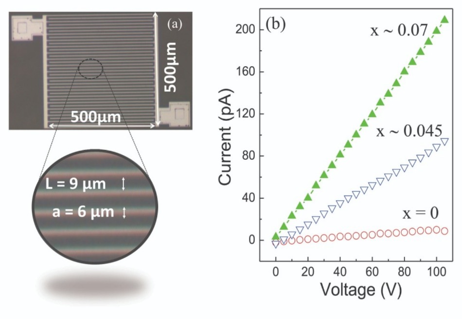
Metal-semiconductor-metal devices (a) with a spacing, L, of 9 mm, and a width, a, of 5 mm, have been used to determine the relationship between the gallium content and the conductivity of the alloy (b).
It is expected that increasing the gallium content would increase conductivity, given that BN is highly insulating, while unintentionally doped GaN is usually conductive. Measurements confirm this, with resistivity falling from 5 x 10¹⁰ W cm for BN to 2 x 10⁶ W cm for B0.93Ga0.07N.
Jiang and co-workers have also produced samples with a 2 nm-thick layer of B0.96Ga0.04N, sandwiched between BN. Photoluminescence measurements of this, held at 10K, have been compared with spectra from a 2 nm-thick B0.96Ga0.04N epilayer. In the quantum well sample, band-edge emission is blue-shifted by 20 meV, indicating quantum confinement.
Goals for the future include increasing gallium incorporation while minimising phase separation, and controlling impurities in these structures.
“Our immediate plan is to fabricate layer structured BGaN quantum well structures with tuneable optical and electric properties,” says Jiang.
Reference
Q. Wang et al. Appl. Phys. Express 12 011002 (2019)

GaN HEMTs with multiple channels and a tri-gate trim resistance and boost drain current while delivering a high blocking voltage
Today’s HEMTs are failing to fulfil their full potential, because their on-resistance is too high, while their blocking voltage is not high enough. But both of these issues can be addressed with a novel design that features multiple channels and a tri-gate.
Armed with these features, transistors produced by a team from EPFL, Switzerland and the Chinese firm Enkris are nearly halving the on-resistance and trebling the drain current compared with a standard structure, while realising a breakdown voltage in excess of 700 V.
“This structure combines, in a unique way, the three-dimensional electrostatic control and excellent voltage-blocking capabilities of the tri-gate, with the tremendous electric conductivity of the multi-channels, to yield significantly enhanced device performance,” explains team spokesman Elison Matioli.
He and his co-workers have pioneered their devices by building on their considerable experience in developing various forms of tri-gate transistors and diodes.
“Tri-gate and slanted tri-gate architectures revealed promising technologies to increase the breakdown voltage of power devices, reaching the buffer breakdown voltage limit for GaN-on-silicon epitaxy with smaller gate-to-drain distances,” says Matoli.
In the team’s latest report on MOSHEMTs, the tri-gate has been united with a multi-channel architecture, which trims resistance thanks to the parallel geometry. Results recently reported in an Applied Physics Letters paper show that on-resistance falls by 38 percent compared with a single-channel, planar-gate variant.
However, even greater resistance reductions are possible, according to very recent, unpublished work: “Preliminary results indicate a reduction by over three times and five times in lateral GaN MOSHEMTs and Schottky barrier diodes,” reveals Matoli.
The tri-gates are a good match for these parallel channels, as they are ideal for control of the carriers. “Under the correct width of these structures, all the channels can be controlled simultaneously, resulting in a huge increase in transconductance and current density, along with a low on-resistance.”
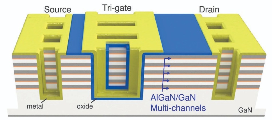
A low on-resistance and a high blocking voltage results from combining tri-gates with multiple channels.
To fabricate the devices, the team began by producing AlGaN-on-silicon epiwafers featuring five parallel two-dimensional electron gas channels, formed from
10 nm-thick AlGaN barriers, 1 nm-thick AlN spacers and 10 nm-thick GaN channels. Electron-beam lithography defined the fins, which were formed by using an inductively coupled plasma to etch to a depth of 200 nm. Electron-beam evaporation and lift-off processes added an ohmic stack of metals for source and drain contacts, prior to rapid thermal annealing in nitrogen at 800 °C.
Atomic layer deposition of 25 nm of SiO2 provided a gate dielectric, which was selectively removed with dilute HF acid in the ohmic regions to expose the source and drain contacts. The addition of a Ni/Au gate contact completed device fabrication.
Measurements on these MOSHEMTs show that compared with a planar device, that with a 40 nm-wide fin exhibits an increase in threshold voltage from -22.3 V to -0.1 V, a reduction in sub-threshold swing from 167 mV/decade to 101 mV/decade, and an increase in transconductance from to 1.6 mS/mm to 29.5 mS/mm.
Switching from the planar control to a variant with a 100 nm fin width and a 50 percent fill factor reduced on-resistance from 11.2 Wm to 6.0 W m and increased drain current from 252 mA/mm to 797 mA/mm.
The team has not investigated the current collapse of its transistors. However, Matioli says that the technologies that have been used by others to diminish the current collapse in HEMTs, such as passivation, source field plates and hole injection, can be applied to their architecture.
He and his co-workers will now optimise the epitaxial structures and device designs of their transistors, to improve DC and dynamic performance.
“Our goal is to fully reach the exceptional capabilities of GaN materials,” explains Matioli.
Reference
J. Ma et al. Appl. Phys. Lett. 113 242102 (2018)
