


When researchers develop a technology, they often do so with a product in mind. But there are times when things don’t work out in the way they intended – and the technology ends up being used in a different manner.
That may well be the case for the technology that engineers at imec have developed to form high-quality III-Vs on a silicon substrate. When efforts started around a decade ago, the ultimate goal was the fabrication of compound semiconductor MOSFETs on silicon.
That effort is still underway, but more recently this III-V-on-silicon technology has also been used as a way to enable the growth of lasers on silicon. That’s important, as improvements in the performance of silicon ICs are now under threat from on-chip and chip-to-chip data transfer rates, which are getting close to their limit. The solution is to switch from electrons to photons – hence the introduction of laser on silicon.
The researchers at imec are producing high-quality III-V material on silicon by a technique known as aspect ratio trapping. Defects are inevitable, due to the signifi cant lattice-mismatch between the silicon and the III-Vs, but these imperfections are annihilated at the walls of the trench. What’s more, by having a V-shape at the bottom of the trench, planes can be selected that prevent anti-phase domains – a destroyer of device performance.
By controlling the growth rates of the III-Vs on various facets, imec’s engineers defi ne the shape of the material that emerges from the trench: it can be rectangular, triangular or hexagonal in nature (see imec’s feature “Gaining an edge with nano-ridges” to discover the details of their craft).
imec’s work on nano-ridge lasers is still in its infancy. So far, the team have produced optically pumped lasers on trenches with widths from 60 nm to 120 nm. By inserting a phase-shift grating, a single-mode emission peak is ensured.
One of the next goals will surely be the progression from optically pumped to electrically pumped lasers. Given the dimensions, success will not be easy. But imec has a great track record in innovation, so I, for one, am optimistic.
Wolfspeed has announced new LDMOS and GaN HEMT product offerings that enable smaller systems with greater reliability and efficiency.
“The acquisition of Infineon’s RF power business has enabled Cree’s Wolfspeed business to transition to the next level of the RF power semiconductor business,” said Lance Wilson, research director at ABI Research. “Historically, Wolfspeed has been a principal player in GaN technology but the addition of Infineon’s LDMOS portfolio has put them into the top echelon of high-power RF.”
The acquisition brings LDMOS technology and expertise to Wolfspeed, enabling the company to provide the optimal RF power solution to meet customers’ needs, regardless of the type of technology used. The expansion includes Wolfspeed’s new 28 V 2620-2690 MHz Asymmetric Doherty Transistor, which is an LDMOS Doherty transistor that uses LD12 technology. This and other LD12 components use a plastic overmold package that delivers the same performance as open cavity packages, offering significant increases in efficiency at a lower cost.
“Wolfspeed is committed to supporting the growth of our LDMOS portfolio, as shown by the release of our new 28 V Asymmetric Doherty Transistor,” said Gerhard Wolf, Wolfspeed’s vice president and general manager of RF.
“The expansion of our LDMOS portfolio delivers on the promise of continued innovation for cellular applications, like improved 4G networks and the shift to 5G networks. In the radar market, Wolfspeed is providing aerospace and defence operators better target discrimination and a longer detection range with the launch of the highest output power GaN products on the market, including a 1200 W packaged GaN HEMT.
The 1200 W GaN HEMT is said to set a new industry benchmark for performance by delivering the highest output power for a GaN L-Band radar product on the market today. The device’s high-output power enables fewer devices to be used, resulting in simplified system architectures, lower materials costs, reduced energy consumption and increased system reaction time that is critical in defense and aerospace settings.
Optical communications firms Acacia and Oclaro are working together to create fully interoperable CFP2-DCO (digital coherent optics) modules based on Acacia’s Meru DSP. Oclaro plans to launch a new CFP2-DCO module that will feature plug-and-play compatibility with the Acacia CFP2-DCO, providing customers with two proven coherent optics suppliers for the 100/200G CFP2-DCO form factor. The modules will support transmission speeds of 100G and 200G for use in access, metro and data centre interconnect markets.
CFP2-DCOs are becoming increasingly important for higher-speed optical networks because they integrate the coherent DSP into the pluggable module. The digital host interface enables simpler integration between module and system resulting in faster service activation and a pay-as-you-grow deployment model for telecommunication providers whereby the cost of additional ports can be deferred until additional services are needed.
“Our 43Gbaud Coherent Transmitter Receiver Optical Sub-Assembly (TROSA) is at the heart of our CFP2-DCO. The TROSA leverages InP PIC technology from Oclaro’s highly successful CFP2-ACO to achieve industry leading optical performance in a small form factor,” said Beck Mason, president of the Integrated Photonics Business at Oclaro. “By establishing a fully interoperable solution with Acacia, our customers will have two sources of supply for these critical components, enabling them to efficiently upgrade their networks to higher speeds.”
The CFP2-DCO form factor is being introduced by multiple network equipment manufacturers in switch, router, and transport platforms.
The CFP2-DCO modules support four times higher density than current generation 100G CFP-DCO solutions by doubling the data rate in a smaller, lower power, pluggable module enabling customers to quickly and cost-effectively roll-out 200G networks.
In addition to proprietary operating modes, both companies intend to support the requirements of the Open ROADM MSA for interoperability at 100G. “Network operators and our system partners are excited about the ramp of our CFP2-DCO module,” said Benny Mikkelsen, CTO of Acacia Communications.
“By partnering with Oclaro to ensure interoperability with their Meru-based CFP2-DCO module, we believe we will be better positioned to address the DCO market as industry trends shift favorably toward the CFP2 form factor. We are excited about our relationship with Oclaro and believe that broader adoption of 200G CFP2-DCO modules will be mutually beneficial to our two companies and the customers we serve.”
Plessey Semiconductors is partnering with Smart Glasses firm Vuzix. The two companies are working to develop the necessary technologies for a new generation of AR Smart Glasses, based around the combination of Plessey’s microLED light source product family, Quanta-Brite, and Vuzix’ extensive expertise and IP in Smart Glasses and essential optic technologies.
Plessey has successfully demonstrated how its monolithic microLED technology can be used to deliver Smart Glasses technology for a wide range of AR and MR (mixed-reality) applications for use both indoors and out.
In addition, Vuzix has already developed an evolving family of Smart Glasses culminating in the Vuzix Blade, the next generation smart display with see-through viewing experience via proprietary waveguide optics.
Formed from glass with precision nanostructures, the waveguide is a key component in an AR/MR product, enabling users to see high-resolution computer-generated graphics, images and information superimposed over images from the physical or real world.

In the development of its next-generation product, Vuzix has selected Plessey’s microLED-based Quanta-Brite light engine, which delivers extremely high efficiency and an improvement in lumen output compared to other light sources currently available on the market.
Quanta-Brite is based on Plessey’s GaN-on-silicon technology, with an integrated monolithic array of RGB pixels with advanced first level micro-optical elements to create a bright, largely collimated and highly uniform light source for the illumination of DMD and LCOS display engines.
The resulting optical system is up to 50 percent smaller, lighter, simpler and cheaper than incumbent solutions and the high performance microLED emitters combined with minimal optical system losses result in significantly increased power efficiency.
Size, weight and power reduction are key considerations in AR/MR wearables. Quanta-Brite has been designed specifically for the next generation of Vuzix personal display systems.
“Plessey’s Quanta-Brite microLED technology can be a major enabler of the future of augmented reality,” said Vuzix President and CEO Paul Travers. “As well as delivering high-efficiency, low-power and small-size illumination capabilities, the very high level of luminescence of the Quanta-Brite light source can also enable the development of end products with a sleeker form factor, which is a key attribute of our waveguide based Smart Glasses and critical to mass market adoption.’
“This development with Vuzix, a leading actor in the exploration of next-generation augmented reality, is a significant endorsement of Plessey’s GaN-onsilicon microLED approach,” said Keith Strickland, CTO at Plessey.
“Monolithic microLED technology is fast emerging as the only one that can provide high luminance in a very small form factor with minimal energy consumption, necessary for reducing costs and enabling lightweight batterypowered products for a range of emerging consumer and industrial applications.”
According to the Consumer Technology Association (CTA), headsets and eyewear outfitted for AR and VR applications are set for record sales this year of $1.2 billion in the US market alone.
Infineon is starting volume production for CoolGaN products by the end of 2018, the company announced during PCIM Europe. Engineering samples of these products are now available.
Infineon’s CoolGaN is claimed to the one of most reliable and globally qualified GaN solutions in the market. During the quality management process not only the device is tested, but also its behaviour in the application.
At 100 ppm (parts per million), its predicted lifetime is about 55 years, exceeding the expected lifespan by 40 years. CoolGaN enables for example doubled output power in a given energy storage slot size, freeing up space and realising higher efficiency at the same time.
Full production of CoolGaN 400 V and 600 V e-mode HEMTs will start by end of 2018. CoolGaN 400 V will be available in 70 mΩ in SMD bottom-side cooled TO-leadless and top-side cooled DSO-20-87 package.
CoolGaN 600 V comes in top-side cooled DSO-20-87 package and bottom-side cooled DSO-20-85. With 70 mΩ and 190 mΩ 600V CoolGaN devices in bottom-side cooled TOleadless and DFN 8x8 packages, the 600V CoolGaN portfolio will be complemented.
Rohm and GaN Systems have announced a GaN power semiconductors collaboration, with the goal of contributing to the continuing evolution of power electronics. This strategic partnership builds on GaN Systems’ capabilities in power GaN transistors along with Rohm’s expertise in semiconductor design and manufacture.
The companies have agreed to jointly develop form-, fit-, and functioncompatible products using GaN semiconductor dies in both GaN Systems’ GaNPX packaging and Rohm’s traditional power semiconductor packaging.
In addition, GaN Systems and Rohm will work together on GaN semiconductor research and development activities to propose ground-breaking solutions for the industrial, automotive, and consumer electronics fields. And to contribute to greater energy savings and increased power densities in the power electronics market, both companies will continue to collaborate to expand their line-up of GaN products and broaden the range of choices.
“GaN has rapidly made its ascent into power electronics applications and this partnership exemplifies how important GaN has become in a complete power electronics offering,” said Jim Witham, CEO of GaN Systems. “We’re proud to partner with Rohm, a company well known for developing industry-leading technologies.
By combining our joint expertise and capabilities, we’re enabling more businesses to access and experience the benefits of GaN in achieving higher power, more efficient, smaller, and lighter power electronics.”
“Rohm has targeted the power device business as one of our growth strategies. We offer leading-edge products such as SiC power devices and provide power solutions that integrate control technologies, including gate drivers that maximise device performance. We are also developing GaN for next-generation power devices. By leveraging the superior technologies and expertise of both companies, we are able to accelerate the development of high-performance solutions to solve the needs of the power market,” said Katsumi Azuma, senior MD of Rohm Semiconductor.
Kaiam, a US manufacturer of advanced data centre optical transceivers, and the Chinese optical module firm Broadex have announced a partnership agreement where Broadex would manufacture and supply high-end transceivers into the China market.
The two companies announced the signing of a memorandum of understanding (MOU) for furthering cooperation on volume production of QSFP28 100G-CWDM4 transceivers based on Kaiam’s LightScale2 platform. The LightScale2 architecture is said to have fundamental advantages in cost and performance and to be ideally suited for high-volume applications. The agreement allows Broadex to manufacture these units in China and directly address Chinese customers who require local production. This also complements Kaiam’s in-house manufacturing in the UK in Livingston, Scotland, and provides further capacity to address the high-volume data centre market.
“We anticipate very strong demand for 100G transceivers based on our LightScale2 technology,” said Dietmar Zapf, GM / VP of manufacturing at Kaiam. “In addition to the production lines already running at our Livingston, UK facility, we need to develop and secure further expanded capacity for manufacturing these products in high volume. The MOU signed with Broadex would allow us to leverage Broadex’s manufacturing expertise and infrastructure and expand our capacity in the next 3–6 months to meet high demand.”
“We are glad that Kaiam chose to continue working with us for manufacturing its new non-hermetic transceivers for data centre applications,” said Yong Ding, VP and CTO of Broadex Technologies. “We have been producing OSA-level components for Kaiam in high volumes for several years now. The LightScale2 platform is optimised to deliver maximum value and performance in the data centre environment at dramatically lower costs. We will work aggressively to quickly ramp to high volumes with high yields.”
“Kaiam is eagerly anticipating expansion into the China market with the assistance of our valued partners at Broadex,” stated Jeremy Dietz, VP of Global Sales and Marketing at Kaiam. “The two companies will combine on business growth activities in and around China to strengthen Kaiam and Broadex’s market share in optical transceivers for data centres as well as PLCs for 5G rollouts.
“The MOU includes details of mutual technology cooperation and manufacturing arrangements on timeline, cost roadmap, local sourcing and China market development.”
UV-Optical sources start-up Bolb, based in Livermore, California, has announced a new line of ultraviolet C-band light-emitting diodes (UVC LED) featuring record single-chip performance for universal disinfection.
For the past two decades, researchers have been stymied by the light-absorbing hole-supplier layer in the device structure of a UVC LED. Attempts at removing this narrow bandgap layer always lead to a significantly degraded current voltage performance, which translates to higher heat generation and shorter device lifetimes. Bolb says its new LEDs featuring the UVC-transparent holesupplying layer do not suffer any voltage tradeoff. This means its packaged LEDs can simultaneously achieve 12.2 percent EQE and 9.5 percent wall-plug efficiency (WPE). For example, 10~11 mW of UVC power can be obtained from a single 0.5 mm by 0.25 mm LED when driving at 20 mA forward current from production LEDs, while maintaining a 5.8 V forward voltage, at an optimised disinfection wavelength of 265 nm to 275 nm. Such a single chip performance is claimed to be to five times that of the competitors’ offerings at similar wavelengths. Unprecedented performance can be achieved with arrays of such emitters, or a single larger emitter designed for higher drive currents according to the company.
The development paves the way for UVC LEDs to achieve efficiencies approaching that of visible LEDs within the next few years, and enables wideranging applications in hospitals, restaurants, packaging plants, agriculture and homes.
At PCIM Europe, GaN Systems unveiled two wireless power amplifiers for the wireless charging market for highpower consumer, industrial, and transport applications. These new solutions include the 100 W power amplifier with ranges from 70 W to 100 W and the 300 W power amplifier with ranges from 150 W to 1 kW.
The 100 W power amplifier [GSWP100WEVBPA] is for applications in the consumer market for items such as laptop computers, recreation drones, domestic aide robots, power tools, and fast-charging of multiple smart phones. The 300 W power amplifier [GSWP300WEVBPA] is targeted for the industrial and transportation markets for applications that include delivery drones, warehousing robots, medical units, factory automation, contractor power tools, eBikes, and scooters.
Both power amplifiers have a range of features including current or voltage control, built-in protection circuitry, EMI filtering, and configurable output power. The amplifiers combine GaN Systems power transistors with high frequency GaN E-HEMT drivers from pSemi.
“Our GaN solutions are creating opportunities for the development of high-power, high efficiency power systems in applications such as wireless power transfer and charging,” stated Paul Wiener, VP, strategic marketing for GaN Systems. “The power ecosystem has changed. There is now availability of high dv/dt level-shifters, fast response IC sensing and control, low-loss high frequency magnetics, and high performing GaN transistor and amplifier capabilities that are enabling smaller, lighter, lower cost, and more efficient power systems.”
At IMS 2018, NXP introduced new RF GaN wideband power transistors and also expanding its Airfast third-generation silicon-LDMOS portfolio of macro and outdoor small cell solutions for 5G.
The new GaN offerings include the A3G22H400-04S wideband power transistor suited for 40 W base stations. It yields up to 56.5 percent efficiency and 15.4 dB of gain and covers cellular bands from 1800 MHz to 2200 MHz. There is also the A3G35H100-04S GaN transistor providing 43.8 percent efficiency and 14 dB of gain. This device enables 16 TX MIMO solutions at 3.5 GHz.
Silicon-LDMOS products include the A3T18H400W23S, a 1.8 GHz device with Doherty efficiency up to 53.4 percent and gain of 17.1 dB. And the A3T21H456W23S, covering the full 90 MHz band from 2.11 GHz to 2.2 GHz. There is also the A3I20D040WN ultra-wideband LDMOS chip offers peak power of 46.5 dBm with 365 MHz wideband class AB performance of 32 dB of gain, 18 percent efficiency at 10 dB OBO. Finally, the A2I09VD030N has peak power of 46 dBm with class AB performance of 34.5 dB gain, 20 percent efficiency at 10 dB OBO.
The RF bandwidth for this product is 575 MHz to 960 MHz.
NXP says that the breadth of its range of RF power technologies – which include GaN, silicon-LDMOS, SiGe, and GaAs – allows product options for 5G that span frequency and power spectrums with varying levels of integration.
Exagan has delivered GaN-on-silicon transistors and switching systems for pocket-sized fast chargers. Rebecca Pool reports.
As the dust settles on this year’s PCIM Europe, myriad power electronics companies are taking home a vast array of GaN-based devices.
For example, GaN Systems showcased 100 V and 650 V GaN E-HEMTs, Transphorm unveiled 650 V GaN FETs while EPC demonstrated its low-voltage enhanced-mode GaN FETs, targeting automotive, power supply and data centre applications, and more.
At the same time, France-based Exagan, also a key power electronics player, launched its 650 V G-FET power transistor alongside an integrated driver and transistor switching system, G-DRIVE, aimed at fast charger markets.
Described as being easy to design into electronic systems, the products are compliant with the USB power delivery 3.0 type C standard. And as Exagan president and chief executive, Frédéric Dupont, puts it: “The market potential here is enormous, including portable electronic devices as well as homes, restaurants, hotels, airports, automobiles and more.”
“In the near future, users will be able to quickly charge their devices by plugging a standard USB cable into a small, generic mobile charger,” he adds.
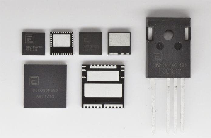
G-GET and G-DRIVE products produce by Exagan are aimed at fast charging markets
Since spinning out of CEA-Leti and Soitec in 2014, Exagan has firmly focused on developing 650 V GaNon-silicon products for photovoltaic, automotive and PC markets and more. So why focus on the charging market right now?
According to Dupont, silicon power devices simply cannot fulfil fast charging applications, opening the door to GaN-based systems. But moreover, the chief executive reckons his company can deliver more intelligent and cost-effective GaN device solutions for this application.
“This is a place where GaN can really have a play, but the challenge is the cost and providing a complete solution – this is why you won’t see many GaN players addressing this segment,” he says. “However, Exagan can bring a lot of value here in the short-term.” Indeed, thanks to a rich heritage of heteroepitaxy development from France-based CNRS-CRHEA, CEALeti, and Soitec, Exagan has been ahead of the pack on production, and consequent costs, from word go.
Indeed, thanks to a rich heritage of heteroepitaxy development from France-based CNRS-CRHEA, CEALeti, and Soitec, Exagan has been ahead of the pack on production, and consequent costs, from word go.
During processing, a stack of buffer, insulating and strain management layers is deposited between the silicon substrate and GaN epi-layers to relieve crystal stresses and prevent cracking.
As a result, Exagan has been able to take GaN-onsilicon FET fabrication to larger wafer sizes, focusing on 200 mm production at X-Fab’s CMOS foundry in Germany, as many other GaN players grapple with smaller, 150 mm wafer sizes.
“Most companies are at six inches today but we have been working at eight inch, which is a good size for GaN,” points out Dupont. “This is important for costs, as most of the silicon power electronics market is currently being manufactured at eight inch... and we are using the same 200 millimetre CMOS infrastructure and equipment.”
“In the future we will see some silicon power devices moving to twelve inches but we think GaN will stick with eight inches,” he adds. “I don’t want to say forever but certainly for a long time as the cost structure is already very competitive.”
Costs aside, Dupont is also certain that GaN-based systems are ideal for fast charging applications. As he points out, heteroepitaxial devices, such as GaN-onsilicon FETs, are fabricated as lateral devices.
“Compared to vertical SiC devices, these transistors are suited to integration and co-packaging,” he says. “So while SiC devices are very suitable for high current and high power applications, GaN is a good choice for fast charging applications and, indeed, any application that can benefit from system in package integration.”
“We have always believed that GaN should be approached as a system solution, rather than a transistor solution, this is why we are offering our intelligent GaN Power solutions to the market” he adds.
And for the future, Dupont says Exagan will be focusing on co-packaging silicon driver ICs with GaN transistors to achieve the best combination of cost, performance and functionality, rather than integrating the driver electronics onto the GaN transistor chip to produce a monolithic IC.
“Customers want to have a whole solution, not just a transistor,” says Dupont. “And they also want to know how to drive it, how to control it, how to design a transformer and so on.”
“We have to make sure our products have what a designer needs for a particular application... and many customers want to use an external silicon driver, this is why we developed G-FET,” he adds. “Meanwhile, some customers and applications need a more integrated solution, and this is offered with G-DRIVE.”
Right now, Exagan is sampling and finalizing application development of G-FET and G-DRIVE products with its customers and will ramp production with foundry partner X-Fab according to demand. The company is also working with TÜV NORD’saerospace and electronics arm, HIREX Engineering, on device testing and qualification in a range of applications.
“The power electronics industry has been very conservative about new technologies but wide bandgap materials – both SiC and GaN – are revolutionizing this space,” says Dupont. “I do hope in a few years you will have a small GaN-based charger in your wallet, that can charge your phone, laptop, and anything you want to charge.”
From data centres to automotives, GaN device maker Transphorm eyes more and more applications as market penetration gathers momentum. Rebecca Pool investigates.
Earlier this summer, California-based Transphorm has launched its third generation 650 V GaN FETs, designed for high-voltage power conversion applications.
Targeting industrial, data centre, renewable and power supply applications, the latest devices offer a 4 V threshold – an industry first for GaN FETs and eliminating the need for a negative gate drive – lower electromagnetic interference and reduced device price.
The latest move builds on a series of critical developments from the company. Transphorm released JEDEC-qualified GaN FETs in late 2016, swiftly following this up with automotive-qualified GaN FETs in March 2017. These were targeting on-board charger and DC-to-DC systems applications in plug-in hybrid and battery electric vehicles.
By May 2017, Transphorm’s 650 V GaN FETs had been integrated to 3 kW AC-DC power supplies from US-based Bel Power Solutions, designed for enterprise reliability server, router and network switching subsystems.
And only months later, Yaskawa Electric was using Transphorm’s 650 V, GaN FETs in its 100 W to 400 W servo motors, designed for the industrial multi-axis automation systems. Yaskawa ploughed some $15 million into Transphorm shortly afterwards, to accelerate GaN product development.
Importantly, earlier this year, Transphorm revealed its GaN FETs are being used in Corsair’s latest power supply unit for gaming applications, as well as Taiwanbased Seasonic Electronics’ high-end power factor correction platform for battery chargers, PCs, servers as well as gaming power supplies.
Past power supply products typically rely on silicon superjunction MOSFETs but by moving to Transphorm’s 650 V GaN-on-silicon FETs, in the typical bridgeless totem-pole power factor correction topology, each company has increased product performance.
For example, Corsair has raised its power supply AC to DC efficiency by about 2 percent to more than 99.4 percent. Meanwhile, the switch from silicon to GaN also increased the power output to 1600 W, some 6.5 percent higher than the previous product generation. Enclosure size was also reduced by 11 percent.
Similarly, Seasonic’s move from a silicon-based platform to one that integrates Transphorm’s GaN FETs raised platform efficiency by 2 percent to more than 99 percent while increasing power density by a hefty 20 percent.
As Philip Zuk, Vice President of Technical Marketing at Transphorm, points out: “Corsair’s power supply is now very, very difficult to buy. The company has seen huge demand for the product from the gaming community and it’s also being used in the supercomputers [that drive] cryptocurrency mining and artificial intelligence applications, which are real power hogs.”
Steps to success
Clearly being in production with Yaskawa, Bel Power, Corsair and now Seasonic, has raised the profile of Transphorm’s GaN FETs. According to Zuk: “This is big news for us... and now, production really is starting to ramp.”
The Transphorm Vice President is keen to point out the development advantages of having products ‘in the field’. As he highlights, the company owns each stage of FET development, and insight gained during customer projects can be applied to its GaN-onsilicon technology to raise FET quality, reliability and performance.
Indeed, Zuk also reckons his company’s transition from first to third generation platform – accompanied by developments in packaging, increases in yield and reductions in die size – has cut costs by some 35 percent.
Importantly, the resulting rising demand for the GaN FETs doesn’t stop with gaming and other niche applications. According to Zuk, the company is now seeing traction from data centres, desperate for efficient power supplies that will help reduce power consumption. He also expects automotive interest will follow.
“Our near-term revenue is being driven by the early adopters, gaming, artificial intelligence, crypto-mining and data centres,” he says. “But ultimately, these niche opportunities will roll-out into less price elastic applications, such as automotive applications, including onboard charging, inverters and DC-to-AC conversion.”
“Indeed, a nice thing about being in production is the actual failure in time [data] we can get, which a lot of automotive customers are looking for,” he adds.
Crucially, Zuk is adamant that Transphorm can scale wafer production alongside rising demand. The company has reactors at sites in Goleta, California, and Aizu, Japan, and anticipates that 6-inch production can boost today’s capacity of 5 million to 10 million parts per year to more than 50 million parts per year by 2020. What’s more, the company has 8-inch production in R&D, and is ready to transition to the larger wafer size with market demand.
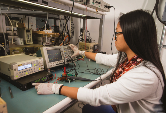
Transphorm has facilities to put its GaN FETs through their paces.
“If we suddenly had to build 50 million parts then that’s a nice challenge to have and we definitely have the capability to ramp to this,” assures Zuk.
Production aside, Zuk is also seeing some technology issues being swept aside. Transphorm’s FETs are based on the so-called cascode topology and from word-go, Zuk has been busy educating industry on the pros and cons of this transistor type versus the alternative enhanced-mode device. “This has been an uphill battle as many [design engineers] have wanted to use e-mode [devices] but I am seeing that barrier come down now,” he says.
Competition from rival technology, SiC, is also key. Rohm and Wolfspeed deliver 650 V SiC MOSFETs, for example, and as Zuk points out, diodes based on this wideband gap material have been in the marketplace for nearly two decades.
However, design engineer reticence on GaN is now dwindling, and this can only propel GaN further into the market. “My competition is not other GaN suppliers, it is silicon carbide, and what has stopped GaN from being more quickly adopted is uneasiness,” highlights Zuk. “But customers have now multiple GaN projects in development and are over this fear-factor.”
Looking to the future, Zuk is confident that silicon, SiC and GaN will co-exist, with decisions largely relying on price pressures and what the customer knows to design in.
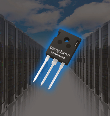
Transphorm’s near-term revenue is being driven by gaming, artificial intelligence, crypto-mining and data centres
Better optics, brighter beams and a higher throughput are propelling cathodoluminescence from the lab to the fab by Jean Berney from Attolight
Our industry prides itself on the production of countless high-quality, reliable devices, which can be degraded at the nanoscale by threading dislocations, stacking faults, inclusions and point defects. Often these imperfections arise during the epitaxial process, due to differences in the lattice or thermal expansion coefficients between the substrate and subsequent layers. However, they can go unnoticed until the end of the line, or even appear in shipped product, where they pose a serious threat to the device’s capability and reliability.
If unnoticed, a killer defect can turn out to be incredibly costly. It is not just the expense associated with undertaking unnecessary production steps on a chip that is destined for failure. The cause of the defect may also need tracing – and when it is exposed, it can reveal a drift in the manufacturing process, and a need to scrap much material. There is also the worst case scenario: chips fail in the field, resulting in angry customers that take their business elsewhere; and the need for expensive failure analysis.
What’s needed is a reproducible, non-destructive defect inspection method that is fast enough for use in production. And at Attolight of Lausanne, Switzerland, we have a cathodoluminescence tool that does just that, the Säntis 300.
Cathodoluminescence is a characterisation technique that involves directing a beam of electrons at a sample, and recording the light that is emitted from it. Much can be resolved, because the electron beam can be focused down to a few nanometres. This allows a sample to be mapped with nanometre resolution, beating light’s diffraction limit by several orders of magnitude. What’s more, cathodoluminescence can be spectrally resolved, offering tremendous insight into material properties (see Figure 1).
Cathodoluminescence is even capable of detecting threading dislocations, a defect responsible for short circuits in power transistors. This may raise a few eyebrows, given that a threading dislocation has a diameter of an atom, and normally it cannot be resolved by an electron probe that is one or two orders of magnitude larger. But cathodoluminescence offers unparalleled sensitivity to defects, due to the light emission process.
In the cathodoluminescence process, electrons that hit the surface subsequently impinge on the semiconductor, slow down and undergo multiple scattering events. Every time there is scattering, electrons within the semiconductor are excited from the valence band to the conduction band to form electron-hole pairs. These pairs eventually recombine, emitting photons in the visible range.
As the cathodoluminescence emission spectrum is directly related to the difference in energy between the valence and conduction bands, it is extremely sensitive to the electronic band structure – and ultimately extremely sensitive to any atomic change or atomic defect. A mere vacancy or dopant inclusion can disrupt the material’s band structure over length scales up to tens of nanometres. Consequently, even though a defect may be far smaller than the electron probe, it affects cathodoluminescence over tens of nanometres, and its presence can easily be detected with a state-of-the-art cathodoluminescence scanning electron microscope.
The emission energy of the cathodoluminescence depends on the nature of stacking faults, local strain variations and point defects, such as dopant inclusions or vacancies. Threading dislocations act as non-radiative recombination centres, quenching cathodoluminescence. Defect sensitivity can be as good as 1016 atoms cm-3, making this, to our knowledge, the most sensitive non-destructive method for uncovering defects.
It is easy to see why cathodoluminescence’s high sensitivity to defects makes it a great technique for performing failure analysis and R&D characterization. However, in a high-volume manufacturing environment, how can it be practical to sample a full wafer every ten nanometres? The good news is that it doesn’t have to be this way, thanks to cathodoluminescence’s greatest weakness becoming its advantage: carrier diffusion.
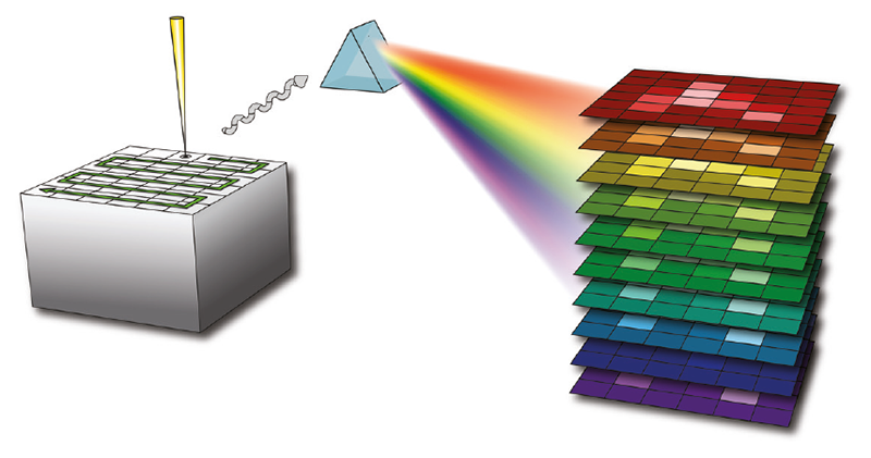
Figure 1. Acquisition of a cathodoluminescence map. The electron beam scans the surface of a wafer. At each point, light is emitted, spectrally resolved so that a hyperspectral map (a map made of multiple colours) is measured.
Carrier diffusion: a curse to a blessing
When electron-hole pairs recombine at the place of generation, cathodoluminescence stems from the precise location of the focused probe. But in a defect-free semiconductor that’s not always the case, as electron-hole pairs can diffuse over hundreds of nanometres before recombining.
At first glance, that suggests that electron-hole pair diffusion reduces the image resolution. But that’s not the case.
Consider a killer defect, such as a threading dislocation. The defect disrupts the local electric field, and traps electron-hole pairs that are nearby. As these pairs cannot diffuse or recombine radiatively, local cathodoluminescence is quenched. For electron-hole pairs generated further from the defect, the chances of diffusing towards it are far less, making radiative recombination more likely. Due to these factors, defects appear in cathodoluminescence images as very small dark spots, limited by the probe size and interaction volume, that fade away over a few hundreds of nanometres.
Sometimes defects may radiate. However, they will always modify the carrier wave function in their vicinity, and provide a distinctive cathodoluminescence spectrum. This may be used to identify a defect or a population of defects, even if they have an atomic size.
Note that a map can even be acquired by spacing out measurement points by hundreds of nanometres. So long as the spacing between measurement points is smaller than the diffusion length, the mapping technique will uncover defects. It is this feature that makes cathodoluminescence the ideal low-sampling technique for spotting loosely distributed defects without having to destroy the sample.
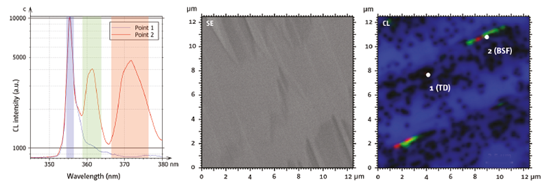
Figure 2. (left) Spectra from point 1 (on a dislocation) and point 2 (stacking fault). (centre) Secondary electron microscope map acquired simultanously to (right) hyperspectral map, having a colour for each defect band. The blue band shows threading dislocations, the green and red band show stacking faults on a GaN template.
A poor reputation
Cathodoluminescence is not a new technique. The phenomenon was first reported as far back as 1879, and cathodoluminescence microscopy has been known since the 1960s. However, use of this technique has been limited to the laboratory, where it has a poor reputation, due to the lack of dedicated instruments.
While collecting cathodoluminescence emitted by the sample is simple in principle, it is not in practice. Difficulties occur, because in the electron microscope that provides the well-defined electron beam, there is competition for the same space by the objective lens of the light and that of the electron microscope.
Up until now, the solution has been to insert a conical mirror, in either a parabolic or elliptical form, into an existing electron microscope.
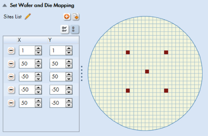
Figure 3. Wafer map showing a wafer with the user defined measurement locations.
One of the many downsides of this approach is that the conical mirror exhibits significant off-axis aberrations, impairing imaging when the wafer is probed anywhere except at the exact focal point of the mirror. Aberrations are so significant that light emitted from the edges of the cathodoluminescence map hits the aperture stop, so it is clipped before reaching the detector – a measurement artefact called vignetting.
Additional drawbacks are that: secondary electron detection is affected by the mirror, making it hard to reach the microscope’s ultimate resolution; and electron microscopes are not designed to work at the optimal conditions for cathodoluminescence, which are a low beam energy and a high current. Instead, a high electron beam current is often traded for a very high resolution at low current.
All these issues have hampered cathodoluminescence, which has a reputation for a lack reproducibility and stability, and lengthy alignment times. These drawbacks motivated us to build the first dedicated cathodoluminescence scanning electron microscope, the Allalin, and its fullwafer counterpart, the Säntis 300.
The latter breaks new ground by bringing cathodoluminescence to high-volume semiconductor production. It has been constructed to produce the highest resolution cathodoluminescence maps possible, and deliver an unprecedented signal-tonoise ratio. Measurement physics, not technology, is the tool’s ultimate limit.
Fantastic features
One of the key features of the Säntis 300 is its entirely new cathodoluminescence collection objective, which has zero off-axis aberration and zero photon loss – allowing for perfectly uniform, reproducible, and quantitative measurements with the highest possible collection efficiency. This approach eliminates alignment time and maximises the signal-to-noise ratio to its physical limit – no matter where the electron probe is placed.
Another attribute of our tool is its state-of-the-art field emission gun technology. The advanced gun trims aberrations by a factor of three and produces higher brightness. A higher probe current is used without compromising resolution. This helps us to dramatically improve the signal-to-noise ratio, speeding cathodoluminescence measurements of weakly emitting specimen, and in some cases making it possible to image a sample.
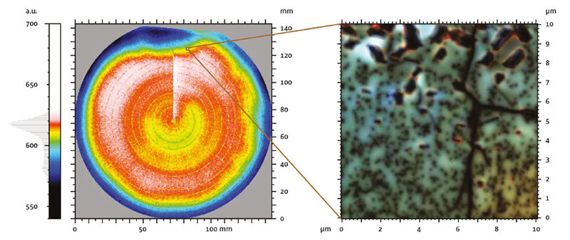
Figure 4. Full-wafer brush image of a 150 mm LED wafer (left) and red-green-blue cathodoluminescence map representation (right).
One of the potential pitfalls of a high brightness gun is that it can introduce unwanted electron-electron interactions. To prevent this, we use a very simple, elegant design that ensures electrons are separated from one another at the source, and don’t interact as they travel to the sample.
We also employ an electron microscope objective lens that leaves a large opening, to allow the inclusion of a high-numerical-aperture light microscope that collects as much light as possible. Our tool is designed so that the optimum focal plane of the electron microscope matches the focal plane of the light microscope. With this approach the user can always work with the smallest probe size.
To realise mapping with sub-micrometre resolution, the beam energy in a cathodoluminescence tool must be below 10 keV. We adhere to this requirement, optimising the objective lens of the electron microscope to deliver a massive electron beam current in the 3 keV to 10 keV range. This is accomplished while maintaining a probe size below 10 nm, to ensure that it takes very little time for users to produce highresolution cathodoluminescence maps.
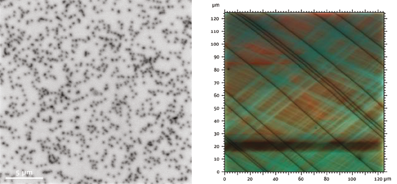
Figure 5. (left) Dark spots corresponds to threading dislocations on a GaN template. (right) Lines represent stacking faults, the dark spot close to the centre is a threading dislocation on SiC.
When we set out to design a quantitative cathodoluminescence detector, one of our primary goals was to maintain the high collection efficiency and spectral resolution when steering electrons away from the optical axis. To accomplish this, we designed a high numerical aperture reflective objective that is optimized to fit in an electron magnetic lens and excel on three fronts: in achromatism, ensuring freedom from colour-related distortion; in aplanatism, to eradicate image distortion; and in thermal characteristics, so that the objective is stable with regard to temperature changes.
Another attribute of this reflective objective is that it avoids the tiny aperture stop, which standard systems use to achieve high spectral resolution at the expense of low light throughput and vignetting.
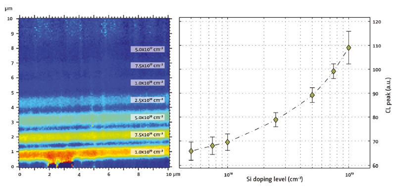
Figure 6. (right ) Graph showing changing silicon-dopant concentration in a staircase GaN structure measured with high precision using cathodoluminescence. In addition, the precise positioning of the electron beam allows to extract optical signatures of small sized areas within a device, non-destructively in top view, or on cross sectioned samples. (left) CL map of the staircase structure.
Thanks to its great design, the Säntis 300 can produce cathodoluminescence intensity maps at a rate of 100 ns per pixel, while realising a dynamic contrast of two-tothree orders of magnitude with materials with adequate emission efficiency, such as III-Vs with a direct band gap. This throughput is sufficient for characterising layers in a high-volume semiconductor fab.
It is worth noting that the Santis 300 system is capable of more than just cathodoluminescence. In its most powerful configuration, it also offers: scanning electron microscopy imaging; UV-visible and nearinfrared hyperspectral imaging, including an individual pixel optical signature; and panchromatic fast imaging (see Figure 2 and 8 for simultaneous scanning electron microscopy imaging and hyperspectral imaging).
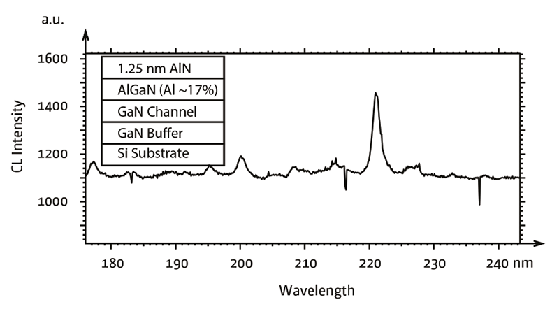
Figure 7. Cathodoluminescence spectrum of 1.25 nm thick AlN etch stop layer. The Säntis 300 is UV capable and sensitive enough to measure spectral signatures over very thin layers that emit photons in the UV spectral range.
Modes of operation
Another feature of the Säntis 300 is its three acquisition modes: step and repeat, across wafer pixel, and full wafer brush.
The step and repeat mode is the one that is most likely to be used in a high-volume fab for non-destructive control of buried defects. When the tool operates in this mode, the user specifies a wafer map by predetermining a list of measurement locations (as shown in Figure 3) that will be investigated and specifies acquisition parameters. The tool then sequentially loads wafers, focuses the electron beam onto them and acquires, simultaneously, secondary-electron and cathodoluminescence maps at each measurement location. Wafers are repeatedly characterized, allowing statistical process control at the highest possible spatial resolution for characteristics such as the distribution of defects, their size, and their spectral signature.
If engineers need to carry out in-depth analysis, they can produce hyperspectral cathodoluminescence maps from wavelengths as short as 200 nm in the UV to 1700 nm in the mid-infrared, using over a thousand channels – or colours – per pixel. Alternatively, they can acquire fast single-channel maps.
Running in the across wafer mode, the Säntis 300 operates with a medium electron-beam spotsize and produces cathodoluminescence intensity maps of full wafers or partial areas of wafers. Operating in this manner takes full advantage of optical signature acquisition. Variations of material across the substrate can be detected. Two hours are needed to map a 150 mm wafer, and partial scanning is proportionally faster.
Engineers will primarily use the across wafer mode for non-destructive process development. This includes efforts at yield improvement, which target uniformity characterization. Studies are related to the likes of buried defect density and impurity variations. Success that results from this approach includes faster development cycles and shorter ramping times.
Operation in the third mode, full-wafer brush, involves defocusing the electron probe and measuring the whole wafer with a low spatial resolution – it is 300 μm. Full 150 mm wafers can be measured in about 13 minutes. This approach generates a massive hyperspectral map of the wafer, enabling a measurement of the variation of material composition across the substrate (see Figure 4).
One of the powerful features of the full wafer brush mode is that it allows an engineer to set upper and lower control limits on the input signal – this enables automatic identification of step-and-repeat locations, which require high-resolution characterization. Operated in this manner, the statistical process control of the Säntis 300 can be extended from optical characteristics and image analysis to X-Y location acquisition coordinates. This allows process profile wafer mapping to be inferred and used as an additional parameter for non-destructive production control, with a fast feedback loop to the process tool.
A versatile tool
As defects are an issue for the production of any device, our Säntis 300 can make a valuable contribution in fabs that are manufacturing LED, microLEDs, SiC and GaN power and RF chips, photovoltaics, and III-V photonics. For all these devices, substrates and epitaxial layers are the base of the pyramid on which devices are built. It is challenging to detect sub-surface defects with nanometre resolution on substrates with diameters up to 300 mm, but the Säntis 300 is up to the task: it can specifically recognize, isolate and quantify most of the defects of interest, including buried defects.
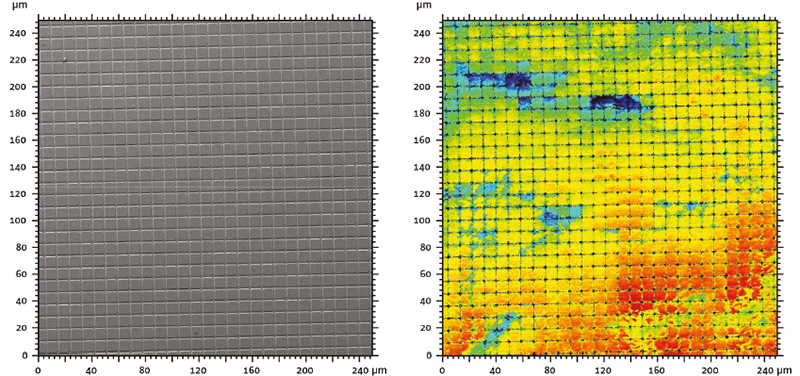
Figure 8. Intermediate process check. (left) Secondary electron map measured simoultanously to (right) hyperspectral cathodoluminescence map showing wavelength shifts over more than 700 microLED structrures.
Our tool is capable of rapid measurements and automatic counting of threading dislocations in a GaN or SiC blanket layer, for densities up to 5 x 109 cm-2. In the example shown in Figure 5, 882 dislocations are identified in a scan area of 25 μm by 25 μm, corresponding to a density of 3 x 108 cm-2.
Even if a layer does not emit light, it might absorb light coming from sublayers and could be indirectly observed this way. This issue can be addressed by cathodoluminescence mapping where the Säntis 300 provides pinhole detection of a non-luminescent layer on top of a luminescent layer.
The optical signature returned by cathodoluminescence is heavily influenced by the type of impurity, and by the level of doping or the impurities in a material. However, characterisation of doped areas is possible with the Säntis 300, according to cross-correlation studies with other techniques, such as secondaryion mass spectrometry (see Figure 6, variations in the emission peak can directly be correlated with the doping concentration. The silicon-dopant concentration can be inferred with high precision).
Thanks to the precise positioning of the electron beam, optical signatures can be taken from smallsized areas within a device. This can be a top-view, or if destruction of the sample is permitted, a profile of the cross-section.
Plasma etching plays its part in the manufacture of many devices. Unfortunately, it can introduce defects on landing layers or impurity loading on a sidewall. These imperfections can be picked up with the Säntis 300, which can also assess the integrity of an etch stop layer (see Figure 7).
One of the most challenging devices to characterise is the micro-structured LED array. That’s because conventional optical methods have insufficient resolution. What’s more, a series of process steps produce a structure that is influenced by interactions that cannot be accounted for during the characterization of a particular step.
Addressing these issues is the Säntis 300, which can perform the critical intermediate process checks. In addition, it allows engineers to determine process uniformity over large fields with high spatial resolution – this holds the key to yield improvement and faster process development (see Figure 8 for an example of imaging microLEDs with the Säntis 300).
For emitting devices, such as LED and lasers, a full wafer scan can be performed using pre or post singularizing of the dies. During this measurement, undertaken at either room temperature or at the functioning temperature of the device, the electron beam activates the device, while optical collection fully characterizes the wavelength, intensity and other parameters of interest. Adopting this approach allows rapid sorting of the die.
Our examples of the use of the Säntis 300 offer an insight into the versatility and importance of quantitative cathodoluminescence. We believe that the launch of this tool promises to revolutionise material characterisation in compound semiconductor fabs all over the world.
Technavio’s analyst for research on lighting, Sunil Kumar Singh, argues that LED chipmakers are not finding it easy due to overcapacity, thin margins and partial commoditisation of the device interview by Richard Stevenson
Q - Is the LED now a commodity market?
A - LED lighting is becoming a commodity. For street lighting applications, or LED light bulbs that are replacing conventional lighting sources, there is a little commoditisation. But for backlighting applications, for automotive, this is not a commodity market right now.
Q - What is the LED market worth today, and how will it evolve in the coming years?
A - The LED market is growing at less than ten percent, and the current valuation is $25 billion to $30 billion. There are three major applications: one is [general] lighting, the second is automotive lighting, and the third is backlighting.
The general lighting market includes LED replacement of conventional lighting sources and street lighting. These are growing. This is why the trajectory of the LED market is growing at a little over ten percent.
The valuation of the LED lighting market is close to $45 billion to $47 billion, and the overall general lighting market is over $90 billion. So the proportion of LED lighting is more than 50 percent of the overall revenue generated. But this proportion will go up from 50 percent to 60 to 62 percent post 2020, and by 2025 it will contribute 80 to 85 percent. So this is a good trajectory for LEDs.
LED penetration in automotive is increasing, as many of the mid-range automobiles are also integrating LEDs for interior and exterior lighting.
The display industry is growing at a slower pace, and backlighting, because of the reduction in the selling price, has actually declined. Sales of portable PCs are declining, and large-area displays are also declining. Demand from emerging applications such as video walls and digital signage is expected to contribute to the backlighting market. However, the volume shipped for these emerging applications will not be very high.
The majority of low-cost devices are [deployed in] a standard back-lighting unit. They have LEDs, but the volume shipped is getting less. So that’s another reason why LED lighting will be a bigger market than backlighting.
We have ultra-high definition TVs coming, and Samsung is getting out of the OLED market and manufacturing quantum dot TVs, so some are saying that the backlighting market may grow. But there is still a decline in the average selling price of the devices.
Q - What are the emerging applications?
A - Horticultural lighting is one of the areas. We also have applications such as LED light strips – that market is gaining good growth. And we have architectural lighting, which has been one of the contributing sectors of the LED industry for much time. But there is still a lot that is happening in this space.
There are also LED wallpapers, portable lighting and LED watches. There is also accent lighting, and LEDs used with IoT devices.
Q - There was a time when ‘the big five’ ruled the LED market. How would you describe the current fortunes of Nichia, Toyoda Gosei, Cree, Lumileds and Osram?
A - When it comes to companies like Toyoda Gosei, Cree, Osram, and Nichia, they are big vendors. It’s just that LEDs used to be manufactured by very few vendors, and now they are manufactured by many vendors.
Now we have LED lighting vendors such as Philips, GE Lighting, Stanley Lighting, Acuity Brands Lighting, Hella, Zumtobel Group, Eaton, Everlight, Seoul Semiconductor, Innotek, Kyocera, Bridgelux and Dialight. Some of these are renowned names in the LED lighting industry, and some of them also have end-to-end solutions of LEDs, right from LED chips to various LED lighting products manufactured in-house.
For lighting, the chip design and the chip making are not the final products – the final product is the LED luminaire. So the success in these particular industries depends on how well one can control the overall value chain of the industry. So a company that has big chip manufacturing and limited customers is finding it tough against a company that is manufacturing the chip and the final product.
At one time Cree, Nichia, Toyoda Gosei, Lumileds, Osram and Souel Semiconductor had up to 70 to 80 percent market share, but now all these vendors put together have less than 50 percent market share. So we are talking about high fragmentation in this market. But these [big] vendors are operating in all the sections of the market, from manufacturing LEDs to luminaires, so they are controlling their own supply and distribution, and are selling their own lighting products.
Q - These companies devoted much effort to protecting their IP. How important is IP today?
A - IP is very important. But it’s not just to do with the chip design – it can also be the manufacturing process.
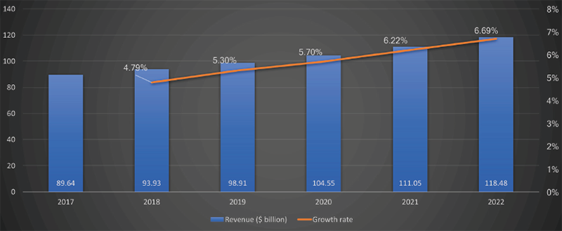
The rate of growth in the global general lighting market will pick up slightly over the next five years, according to Technavio.
Q - Is there much to be gained by offering class-leading LEDs today? Or is cost the key?
A - The cost is the main thing. The cost of the product includes that of the LED package, the optics, mechanical/thermal components, assembly, and the LED driver. Of these, the LED driver attracts the highest cost, followed by manufacturing, mechanical/thermal components and others.
For manufacturing, the back-end process contributes more than 50 percent of the overall production cost, followed by the phosphor, substrate, epitaxy, and wafer processing.
The cost of the chip back in 2013 or 2014 was a little above a dollar. There are two factors behind its decline. One is the overcapacity of LED chips, that has forced all vendors to reduce the price; and the other is the manufacturing efficiency.
The cost of an LED chip has gone down to less than $0.60 per unit for LEDs, and close to $0.80 per unit for high-brightness LEDs.
Q - How dominant is China today in LED chip manufacturing?
A - China is dominant when it comes to chip manufacturing. Look at the number of fabs that have been established. Back in 2008, China had close to 28 fabs. In 2016 it was in the range of 70 to 75 fabs, and now it will be even more than that. The total number of fabs in the world is in the range 170 to 180.
Q - Is there much consolidation within China’s LED chipmaking sector?
A - No. There is not much consolidation. Consolidation is happening at a very slow rate. Very small players get acquired or merge. Bigger companies such as Cree and Nichia have acquired small vendors.
Q - Are companies within China making much profit?
A - We studied the LED market in China back in 2016. We looked at two scenarios: whether companies had subsidies from the government; and what would happen after the subsidies went. Since then we have been tracking that market.
When companies had subsidises between 2011 and 2015 – during the twelfth five-year plan, which was directed at energy efficiency, with the government wanting LED companies to be established – profits were close to 8 percent to 10 percent. But, now after the subsidies are over and the companies are on their own to supply chips, profits are reduced to 5 percent to 7 percent, and for some companies 2 percent to 3 percent.

The LED lighting market will deliver double-digit growth over the next few years.
Q - Veeco shipped many of its K465i MOCVD tools to China in 2009 and 2010. Given the overcapacity that followed, and investment in new tools, is there a big market for second-hand MOCVD tools?
A - There was always a demand for Veeco tools in 2009 and 2010. But we are talking about a time for two-inch epitaxy. Now the path, for the majority of investment is four-inch. And after that it’s six-inch.
MOCVD tools from 2009 and 2010 have a life cycle of seven to ten years, depending on the application. So these tools do not have much of a second-hand market. In the 70 to 75 fabs in China, there is no demand.
Q - For sales in China, are Chinese makers of MOCVD tools, such as Amec and Topec, about to overtake Veeco?
A - Amec’s Prismo D-Blue MOCVD platform is gaining popularity among the customer base of LED chipmakers, as it delivers high-volume manufacturing of GaN, InGaN and AlGaN ultrathin layered structures required for highbrightness LEDs. Topec is one of the market participants focusing on developing MOCVD equipment domestically.
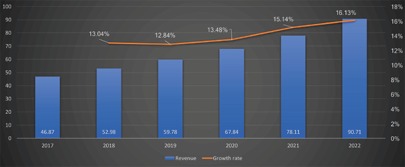
The global general lighting market will continue to be dominated by residential and commercial lighting.
Q - What is the most common platform for making LEDs? Is it now 6-inch sapphire?
A - The majority is now 4-inch.
Q - Who are the leading suppliers of sapphire substrates?
A - Some of the companies are Rubicon Technologies, Crystal Applied Technologies, Precision Micro-optics, Monocrystal, Kyocera, Crystalwise Technology, TeraXtal Technology, DK Aztec, Gavish, and Hansol Technics.
Q - How common is the use of patterned sapphire?
A - Patterned sapphire suppliers include Rubicon Technologies, Sinopatt, Jing’An, Rigidtech, ECEC, and Crystal-Optech. Rubicon have their complete product line as patterned sapphire. But there are some other vendors that have a product mix.
The GaN HEMT is now a formidable, mass-produced device, combining great efficiency with excellent reliability and robustness. By Richard Stevenson
If you spend all of your time looking forward it’s easy to lose sight of how far you’ve come.
That’s a trap that many of us can fall into when we are considering the variant of the GaN HEMT that operates in the RF domain. Often, the future is the focus – sales are tipped to rocket to more than a billion dollar per year by the start of the 2020s.
Take that perspective and it’s easy to forget the progress that has been made to date. It is now more than a decade since the launch of the first GaN HEMT operating in the RF, and over that timeframe devices have been deployed in many different applications. And now, revenues are significant. According to market analyst Yole Développement, GaN RF device sales to the military will net $201 million this year, while those for base stations and satellite communications will accrue $150 million and $29 million, respectively.
A snapshot of how far the GaN RF industry has come, and the challenges that lie ahead, was provided at this year’s CS Mantech, held at the Hyatt Regency in Austin, TX, from 7-10 May. That meeting featured a session on RF devices that included presentations detailing: the creation of E-mode and D-mode HEMTs, via variations in the form of stress in the device; the development of an efficient 15 W/mm GaN technology for serving pulsed radar in the C-band; improvements to a 0.25 μm process for radar and 5G applications; and opportunities to refine the mass production of high-reliability GaN HEMTs for wireless communication.
The benefits of stress
One of the biggest weaknesses with GaN technology is the lack of truly normally-off enhancement mode and depletion mode integrated devices. Due to the chemical inertness of GaN and its alloys, etching is not easy, and it often leads to an increase in the gate leakage in enhancement-mode devices. An alternative, fluorine implantation, also introduces damage to the semiconductor material, thereby impairing reliability.
A very promising solution, described by Konstantin Osipov from Ampleon, involves the addition of a SiN passivation layer. This applies stress to the AlGaN barrier – which is under tensile strain due to lattice mismatch – and it ultimately controls the density of the two-dimensional electron gas under the gate region (see Figure 1). Armed with this lever, the team can realise either partial or complete depletion of the transistor channel, and thus fabricate enhancement and depletion mode devices on the same wafer.
According to Osipov, introducing the SiN layer also produces a reduction in the gate leakage current and the elastic energy stored in AlGaN at the drain side of the gate. “So theoretically, [our technology] should lead to significant reliability improvement.”
Development of the technology can be traced back to efforts by Osipov to reduce the gate leakage current with SiN layers with different compositions. This trial revealed that differences in SiN composition led to variations in the threshold voltage.
“I’ve tried to understand the physical reason behind this phenomenon,” explains Osipov. “The only reasonable explanation that I’ve found is internal compression in the silicon nitride layer that is transferred to AlGaN.”
After confirming this assumption with simulations, Osipov went on to create a simulator virtual enhancement-mode device that featured highly compressive SiN. After this, he developed an experimental process for making integrated enhancement-mode and depletion-mode devices.
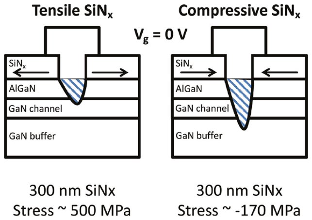
Figure 1. Adjusting the strain in SiN can lead to depletion in the channel of the GaN HEMT, and a shift in the threshold voltage by more than 1 V.
Note that the use of external stressors is actually a tried and tested technology. “In silicon technology, external stressors are used for electron and hole mobility enhancement, despite the fact that silicon is not even a piezoelectric material,” says Osipov.
Fabrication of the team’s devices began by loading 4-inch, n-type SiC substrates into an MOCVD reactor and growing an iron-doped buffer layer, an unintentionally doped GaN channel, and a 10 nmthick Al0.26Ga0.74N channel. After adding a Ti/Al metal stack to form ohmic contacts, a 300 nm-thick SiN passivation layer was grown across the whole wafer (see Figure 2(a)).
The next steps involved: using photolithography and etching to open windows in the passivation layer where enhanced-mode HEMTs would be formed; depositing a compressive SiN layer over the whole wafer, before using photolithography and etching to remove this at locations where depletion-mode devices would be added; and then using a sputtering process to compete fabrication of 100 nm gates.
Measurements of DC characteristics revealed that there is a threshold difference of more than 1 V between the enhancement mode and depletion mode devices. For the enhancement mode HEMTs, DC performance is claimed to break new ground, in terms of on-resistance, peak transconductance and gate leakage.
The researchers attribute this success to their technology. One of its merits is that it produces a ‘virtual’ gate recess effect, while maintaining the thickness of the AlGaN barrier. Another virtue is that the sputtered iridium process, developed at FBH, avoids damage to the semiconductor surface during fabrication. Thanks to this, the devices exhibit ideal normally-off behaviour and avoid any trade-off between AlGaN thickness and threshold voltage – that can lead to low parasitic input and output resistances.
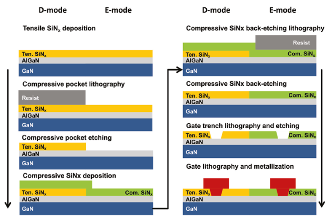
Figure 2. The team from Ampleon and FBH Berlin have produced E-mode and D-mode HEMTs side by side with a process that includes the deposition of tensile and compressive layers of SiN.
One weakness of the enhancement-mode devices is that they can be compromised by back etching of the tensile SiN layer. However, this issue can be avoided.
“Technically it’s not a problem to leave a few tens of nanometres of tensile silicon nitride and cover it with a compressive film,” says Osipov. “In this case, compression from the thicker layer will easily overcome the tensile stress of silicon nitride underneath, and the overall stack stress will be compressive.”
The team have made some RF measurements. “The damage from tensile silicon nitride removal negatively influenced RF performance of E-mode transistors,” admits Osipov. However, the cut-off frequency for these devices is still higher than that for depletionmode variants.

Figure 3. Scanning electron microscopy images of Integra Technologies’ 0.25 μm GaN die design that has a breakdown voltage of more than 250 V.
Empowering pulsed radar
For radar systems used for weather, air traffic and the military, the most desirable attributes for an amplifier are a high output power and a high efficiency. While those made from GaN HEMTs are already delivering a performance that is good enough to serve in many of these applications, there is demand for an even higher efficiency – this could trim the size, weight and power dissipation of the electronics, and lead to smaller, lighter and more efficient systems.
The key figure of merit for the HEMT is its power density, which is the product of its current density and the bias voltage. For AlGaN/GaN HEMTs, for typical bias voltages of 28 V to 50 V, the current density tends to peak at around 1 mA/mm. This can be doubled by switching to more novel material combinations, such as InAlN/GaN, InAlGaN/GaN and N-polar GaN. However, due to the conservative nature of the radar industry, it can take more than ten years to transform a laboratory technology into an approved product. Given that hurdle, there is much to recommend to any approach that offers a shorter path to technology maturity.
At Integra Technologies of El Segundo, California, they are adhering to that view, and using voltages of up to 100 V to increase the power density.
At CS Mantech, company spokesperson Gabriele Formicone provided an update of the company’s latest progress. He argued that two of the most important breakthroughs have been the higher power densities and the higher impedance, aiding broadband matching. However, the pinnacle of the team’s success, according to him, is the realisation of a power density of 15 W/mm at C/X-band, using a production-ready GaN-on-SiC technology. “[This] is much more cost effective compared to alternative approaches, among which is GaN on diamond.”
Migrating to higher voltages will not be an issue in the radar sector, which has traditionally used travelingwave tubes. “100 to 150 volts is still orders of magnitude safer than 10,000 volt traveling-wave tubes supplies,” says Formicone. “Therefore, we do not see any downside in migrating from the nominal 28 volt to 50 volt power supply to 100 volts to 150 volts in high-performance radar, electronic warfare and industrial, scientific and medical applications.”
The team’s latest results were obtained with its 0.25 μm GaN-on-SiC HEMT process, which produces devices with a breakdown voltage in excess of 250 V. Chips are housed in a ceramic package, and performance evaluated at 7.9 GHz using 35 μs pulses and a 10 percent duty cycle – these operating conditions are claimed to be of interest in some radar remote sensing applications.
Using a 90 V bias, devices can deliver 150 W with 11 dB of power gain. Operating in this manner, drain efficiency is 50 percent, corresponding to a power-added efficiency of 46 percent. Crank up the voltage to 100 V and there is little improvement in output power, but drain efficiency still exceeds 40 percent.
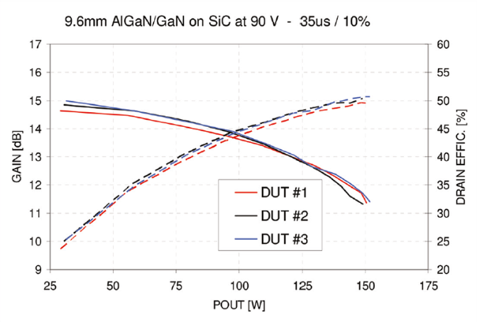
Figure 4. Measurements were made on three of Integra Technologies’ 9.6 mm GaN-on-SiC HEMTs, operated under 90V bias. Testing took place at 7.9 GHz, using a pulse width of 35 μs and a duty cycle of 10 percent.
The lack of improvement is explained by the 100 V device being a first iteration. “An improved design would show good performance at 100 volts too,” argues Formicone. “Additionally, as voltage increases to 100 volts, load impedance tends towards 50 ohm, which requires a more careful test fixture/circuit design to properly match, given the narrow width of the transmission lines.”
Integra will extend this technology to even higher voltages. Benefits will not be limited to a smaller, lower cost die for a given power level, but will extend to improved broad band matching.
The move to higher voltages should not prove too tricky, as Integra is not heading into uncharted territory – at lower frequencies, it has already produced parts that operate at 150 V and offer efficiencies of 80 percent. “At higher frequency it is always a bit harder,” says Formicone, “but Integra has been pursuing this technology roadmap for a few years already with very interesting results.”
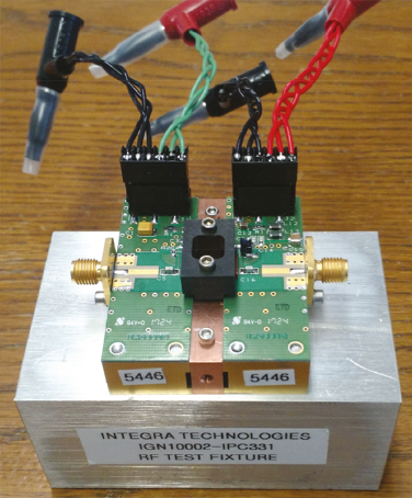
Integra’s AlGaN/GaN X-band FET.
Refining the process
At WIN Semiconductor, efforts have been underway to improve the performance of GaN-on-SiC MMICs fabricated on a dedicated 100 mm line. These devices are targeting radar and 5G applications.Refinements to the company’s 0.25 μm process, described to delegates at CS Mantech by Yi-Wei Lien, have increased small signal gain by 1.8 dB to 20.3 dB and driven up the power-added efficiency at 10 GHz from 59.6 percent to 64.7 percent.
Higher levels of performance are claimed to result from a combination of a superior epitaxial process and optimisation of the processing. Thanks to these advances, there are reductions in gate-lag and drainlag by 25 percent and 11.6 percent, respectively. That’s a big deal, because it implies that there are fewer traps, and ultimately a reduction in the current collapse of the transistors.
GaN MMICs produced with the latest process are also free from a kink-effect that plagued the previous generation. The kinks, seen in DC measurements of the source-drain current as a function of drain-source voltage, are associated with hot electrons – they are trapped at a low drain-source voltage and de-trapped at a higher voltage.
Another improvement in WIN’s technology has been the integration of the RF power amplifier with an RF switch, in the form of a symmetric transistor with a 0.25 μm gate located at the centre of the source-drain region. Testing, using a pulse width of 50 μs and a duty cycle of 10 percent, reveals a rise time of 36 ns and a fall time of 13 ns.
In addition to these impressive switching speeds, the switch is reliable. High-temperature reversebias testing at -50 V and 150 °C reveals that during 1000 hours of operation, the switch’s on-resistance, threshold voltage, and the saturation drain current vary by less than 12 percent.
High-volume manufacturing
From the perspective of Sumitomo Electric Device Innovations, the GaN HEMT is now, without doubt, a device in mass production. At CS Mantech, company spokesman Fumikazu Yamaki emphasised this point by reporting developments in robustness and packaging.
To ensure that a product can offer many years of service, it needs to combine high reliability with a high degree of ruggedness – a capability to cope with operating conditions beyond those that were intended. Yamaki and co-workers have devoted much effort to realising this, evaluating progress in terms of increases in the safe operating area. For a GaN HEMT with an intended drain-source voltage of 50 V at 2.1 GHz, the peak drain voltage during operation can hit 160 V, but the breakdown is still far higher: it is 220 V. Thanks to this margin, it is argued that the device has sufficient ruggedness for mismatched and unexpected load impedances.
Reliability of the company’s HEMTs is also very high, with DC high-temperature operating life tests revealing a mean-time-to-failure of 23 million hours at a channel temperature of 200 °C. Note that in base stations, high power amplifiers may have channel temperature this high.
One recent development at Sumitomo is the housing of devices in plastic packages, which are needed to meet the cost and size requirements associated with 5G. In these packages it is essential to include die level humidity protection. An improved surface passivation film can provide this, according to Sumitomo’s 200 hour tests at 130 °C using relative humidity of 85 percent.
These efforts at Sumitomo underline the progress that has been made with the GaN HEMT. It is a fully fledged commercial device, and with further progress being made by not only this Japanese outfit – but also the likes of Integra, Ampleon and WIN – there is good reason to believe the positive forecasts of the market analysts.

Aspect ratio trapping enables the fabrication of nano-ridge lasers on silicon substrates by Bernardette Kunert, Robert Langer, Marianna Pantouvaki and Joris Van Campenhout from IMEC and Dries Van Thourhout from Ghent University

Figure 1. Cross-sectional, scanning electron micrograph images of cleaved GaAs nano-ridges. (a), (b) and (c) show GaAs nano-ridges on top of 100 nm, 40 nm and 20 nm wide oxide trenches, respectively. All structures were deposited in a single growth. (d) a tilted top-view scanning electron micrograph image of an nano-ridge array on top of 100 nm-wide trenches. Some of the images are modified and reprinted from B. Kunert et al. Appl. Phys. Lett. 109 091101 (2016) with the permission of AIP Publishing.
Maintaining the march of Moore’s law is getting more and more difficult. In recent times, it has required the introduction of novel geometries and esoteric materials, such as hafnium dioxide. And in the years that lie ahead, progress may hinge on the use of III-Vs – either as a material for adding on-chip RF-functionalities, or for providing a light source that speeds on-chip and chip-to-chip communication.
Requirements for the integration of III-V and silicon technologies are more complex than the realisation of good performance. It is essential that the process must also be cost-efficient and suitable for mass production. So, in other words, it must be scalable and compatible with existing IC technology.
The key to cost-efficient, scalable integration is the monolithic hetero-epitaxial growth of III-V layers directly on a silicon substrate. This approach is superior to that of bonding at the wafer, chip and die level. However, the challenge is to develop a technology that can accommodate the latticemismatch between silicon and the majority of the III-Vs. Dislocation defects will arise, due to strain, so they have to be controlled and restricted to a constrained area, to allow the active III-V device layers to be free from defects.
Nano-ridge engineering
At imec, we are trailblazing a unique approach to the integration of III-Vs with CMOS. We are pioneering nano-ridge engineering. It begins by depositing, by selective area growth, III-V material inside narrow oxide trenches that are formed on patterned 300 mm silicon substrates. Further growth of III-Vs creates nano-ridges.
This approach may appear esoteric, but it is not – it is compatible with standard processes used in the silicon CMOS industry. Patterning of silicon and its oxide is based on the shallow trench isolation process, and the growth of the III-Vs is by MOCVD.
The ingenuity of our approach is that the growth starts with the deposition of III-Vs in narrow trenches with a high aspect ratio – that is the height of the trench is far greater than its width. It’s a technique that is known as aspect ratio trapping (ART), and it is successful with many different hetero-material systems. The geometry of the trench results in a very efficient dislocation trapping at the oxide side walls. Misfit and threading dislocations are constrained towards the bottom of the trench, creating a top region that is free from dislocation defects (more details on how it works can be found in the box “The art of aspect ratio trapping”).
Aspect ratio trapping is particularly beneficial when combined with trenches oriented along <110> directions of silicon. This allows the preparation of a V-shaped silicon surface with two {111} planes. When III-Vs nucleate on a {111} silicon surface, this plane prevents the formation of anti-phase domains, which are detrimental to device performance.
When selective area growth continues, dislocationfree III-V material grows out of the trench. Adjusting the MOCVD growth parameters alters the form of the nano-ridge. For example, growth conditions can be selected to broaden the nano-ridge and thus increase the volume of III-V material, which can provide a foundation for new device architectures.

Figure 2. Left: An illustration of aspect ratio trapping of threading dislocations in {111} planes. Middle: Cross-sectional scanning electron micrograph images of a box-shaped GaAs nano-ridge surface. Right: Annular bright-field scanning transmission electron microscopy (ABF STEM) of a GaAs nano-ridge in cross-section along the trench. The transmission electron microscopy sample volume is also indicated in the scanning electron micrograph image by the red-dashed line. The dark blurry lines in the ABF STEM image are threading dislocations, which are all trapped inside the trench. The V-shaped {111} silicon surface induces a Moiré pattern in the transmission electron microscopy image close to the GaAs-silicon interface.
We have formed box-shaped GaAs nano-ridges on top of 100 nm, 40 nm and 20 nm wide trenches (see Figure 1). This series of growths shows that the fundamental shape evolution is independent of trench size. Viewing these structures from above with a scanning electron microscope reveals that the nanoridges are of high quality and are highly uniform.
Our nano-ridge engineering also has great strength and flexibility. Adjusting the growth conditions enables the shape of the GaAs nano-ridge to be tuned to a tall rectangle, a triangle or various diamond-like shapes. Different structures result from selective manipulation of the growth rate hierarchy of the various nanoridge facets. It is the facets with high growth rate that disappear quickly, while those with a low growth rate define the shape of the nano-ridge (see box “Nanoridge engineering” for more details).
We are not the first to report the shape control of ridges. Others have announced homo-epitaxial selective-area growth of III-Vs on the micrometre scale – this is a fundamental feature of epitaxial growth. We break new ground by applying aspect ratio trapping to hetero-epitaxy of III-Vs on silicon, and realise astonishing control of nano-ridge formation on the nanometre scale.
The effectiveness of aspect ratio trapping is highlighted by images acquired by annular brightfield scanning transmission electron microscopy (see Figure 2). This technique reveals that threading dislocations, visible as dark blurry lines, are restricted to within the trench, while GaAs nano-ridge material, on top of the oxide pattern, is free from these imperfections.
We are currently exploring additional metrology techniques that may provide a better insight into defect statistics. To date, we have a very strong indication that dislocation trapping is extremely efficient in trenches with a width of 100 nm or less for 300 nm deep trenches. Nevertheless, along the nano-ridge length we can see planar defects, such as a micro twin every several micrometres. To eradicate these defects, we are devoting much effort to optimising the III-V nucleation and the pre-cleaning step for the trench-patterned wafer.

Figure 3. (a) Cross-section scanning electron micrograph images of InGaAs/GaAs nano-ridge lasers with an InGaP cap on top of 60 nm-wide trenches. (b) High-angle annular dark-field (HAADF) scanning transmission electron microscopy image of a nano-ridge laser sitting on a 100 nm-wide trench. c) Finite difference eigenmode simulation of the basic transverse electric (TE)-like mode, based on the dimensions of the nano-ridge laser shown in (b). Some of the images are modified and reprinted from Y. Shi et al Optica 4 1468 (2017).
Lasers on the edge
The combination of impressive uniformity of the nano-ridge lines, the smooth surface morphology and a ridge with a width of several hundred nanometres lends itself to the production of a nano-ridge laser, where the nano-ridge acts as an optical waveguide. Working in partnership with Ghent University, we have produced such a device. It features In0.2Ga0.8As/GaAs multi-quantum wells, grown compressively strained on top of the (001) nano-ridge facet; and a lattice-matched In0.49Ga0.51P cap layer, which surrounds the full nano-ridge, ensures carrier confinement and provides surface passivation.
Cross-sectional scanning electron microscopy imaging of our device layer stack, sitting on top of 60 nm-wide trenches, emphasises the impressive continuity from ridge to ridge (see Figure 3 (a)). The InGaP cap layer around the waveguide ridge is easy to identify, and it is possible to make out the positions of the quantum wells.
Greater detail is provided by high-angle annular dark-field scanning transmission electron microscopy. When this is used to image a nano-ridge laser on a 100 nm-wide trench each of its layers is clearly visible. The device also contains a GaPAs layer, which is explored for strain compensation and additional carrier confinement.
The art of aspect ratio trapping
III-VS AND SILICON are lattice-mismatched, so the growth of the former on the latter generates defects. However, these imperfections can be trapped with great efficiency by selective area growth in highly confined trenches oriented along <110> directions of silicon. The key is to use trenches that are far higher than they are wide.
When III-Vs are deposited on patterned silicon/SiO2 substrates, misfit and threading dislocations form during the growth to release strain. A typical relaxation mechanism is the nucleation of dislocation half-loops at the growth surface, which glide down towards the interface between the III-V and silicon to efficiently release the strain.
If the dislocation Burgers vector is based on a 60° misfit dislocation, the slip plane is a {111} plane. Hence, as the dislocation half-loops start to glide down along the {111} plane and extend in width, the two threading dislocation ‘arms’ hit the oxide sidewall and are trapped. This trapping mechanism is easy to follow when the {111} slip plane is perpendicular to the trench sidewalls.
The {111} slip plane can also be parallel to the sidewall. When that’s the case, the dislocation half-loop ‘arms’ finally hit the oxide wall as the trench gets filled due to the inclined angle of 54.7° of the {111} plane, so long as the aspect ratio of the trench – that is its height to width ratio – exceeds 1.43. As aspect ratios for trenches are far higher than this, all dislocation defects are fully trapped in both directions, so long as the relaxation process proceeds via threading dislocations gliding along {111} planes. Success hinges on enhancing pronounced dislocation nucleation close to the interface between the III-V and silicon, to ensure full strain release of the hetero-layer.
Note that stacking faults and micro twins, which are planar defects running in the <111> direction, are only trapped in {111} planes parallel to the sidewalls. Consequently, a planar defect that is running perpendicular to the sidewall could penetrate the full III-V structure. So, to prevent this from happening, planar defect formation has to be eradicated by optimising the growth conditions, the silicon surface pretreatment and the fabrication process for the trenches.
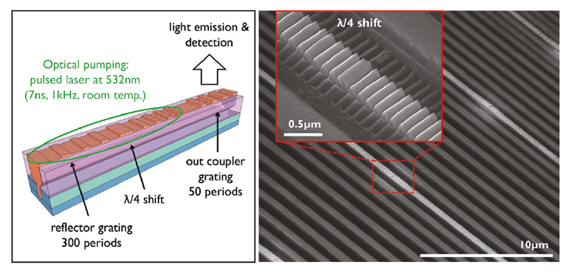
Figure 4. Left: An illustration of the distributed feedback laser design produced by imec, and the excitation geometry using for optical pumping. Right: Top-view scanning electron micrograph image of imec’s fabricated nano-ridge lasers. The inserted, higher magnification image shows the λ/4-phase shift segment between the two reflector gratings.
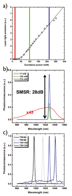
Figure 5. (a) Laser light emission versus excitation power for a distributed feedback nano-ridge laser (170 nm firstorder grating period) on top of a 100 nm-wide trench. The corresponding emission spectra at the excitation power indicated by the red, green and blue lines are shown in (b). Note that the SMSR is the side mode suppression ratio. (c) Comparison of the emission spectrum for a nano-ridge laser based on trenches with widths of 60 nm, 80 nm, 100 nm and 120 nm. The emission intensity is normalized for better comparison. All the plots are reprinted from Y. Shi et al. Optica 4 1468 (2017)
We have modelled the performance of our lasers. Using a finite difference eigenmode solver, we have simulated the basic transverse electric-like mode for our nano-ridge laser (see Figure 3(c)). Results suggest that our device has a confinement factor for the transverse electric mode of 9.3 percent, which is more than sufficient to realise efficient optical gain. Light field losses into the silicon substrates are acceptable, with values less than 5 dB cm-1.
Development of our devices began with the fabrication of distributed feedback lasers at Ghent University. Construction of these edge-emitters that are designed for optical pulse pumping involves processing, into the nano-ridge top surface, a first-order reflector grating with a λ/4-phase shift section. To couple the light out of the waveguide for detection, we add a second-order grating (see Figure 4 for an illustration of the design of the laser, the excitation geometry, the pumping laser conditions as well as top-view images of fabricated nano-ridge lasers).
Due to the narrow spacing of the nano-ridges, we processed isolated, clearly separated nano-ridges. Adopting this approach enabled optical pumping, from above, of a single nano-ridge laser.
Optical pumping of these structures produced a clear threshold behaviour, in line with a pronounced linewidth narrowing of the emission spectrum (see Figure 5(a)). These characteristics are indicative of laser operation at room temperature. As expected for a distributed feedback laser, there is a clear singlemode laser emission above the pumping threshold – in our case, the onset is at 37 mW, equating to a pump density of 33.6 kW cm-2. Encouragingly, the peak emission intensity for excitation at 215 mW is 28 dB above the background, demonstrating excellent single-mode laser performance (see Figure 5(b)).
An interesting attribute of our lasers is that there is a shift in emission wavelength with trench width (see Figure 5(c)). The shift, which may be useful in certain applications, stems from a change in nano-ridge volume.
Even though our work is in its infancy, it shows great promise. As the epitaxial growth conditions govern nano-ridge engineering, it can be applied to a multitude of device architectures and designs. This means that our laser diodes don’t have to be restricted to designs made from InGaAs and GaAs – the door is open to pursue many new opportunities. With this in mind, while undertaking ongoing development of our nano-ridge lasers towards current injection, we will also be actively exploring nano-ridge engineering of different III-V material systems and device applications. So keep a look out for our next success, which we will soon report.
Nano-ridge engineering
APPLYING APPROPRIATE deposition conditions, and exploiting differences in growth rate on different facets, hold the key to III-V nano-ridge engineering. When a free-standing nano-ridge grows out of a trench, it contains several facets, exposed with different III-V surface configurations. For example, when GaAs is grown in trenches with V-shaped {111} silicon surfaces, they have normally a polarity that reveals a gallium-terminated top {111}Ga and an arsenic-terminated lower {111}As nano-ridge plane. For the surface configuration on {110} and (001), the situation is markedly different.
Surface reconstruction on the different facets is determined by the MOCVD growth conditions, such as the growth temperature, reactor pressure, precursor partial pressure and gas phase ratio. The rate of growth of any facet is determined by the precursor diffusion length, and the adsorption and desorption rates. Modifying the deposition conditions increases the growth rate on some facets, slows it on others, and ultimately controls the geometry of the nano-ridge. As the facet with the highest growth rate disappears quickly with deposition time, the shape of the nano-ridge is defined by the facets with lower growth rates.
Highlighting the impact of different growth conditions are cross-sectional scanning electron microscopy images, shown in the figure below. The trench formed in (a) results from a very high GaAs growth rate on the {111}Ga facets, a medium growth rate on the (001) plane and a very low deposition rate on the {110} and {111}As facets. Due to these conditions, the nano-ridge evolves into a rectangle with a high aspect ratio.
With structures (b), (c) and (d), the conditions have been modified to manipulate the growth rate hierarchy in a different way (note that the size of the red arrows in the figure indicates the strength of the growth rate on the different facets). For structure (b), the (001) facet disappears, while in (c) the {110} facet vanishes, and in (d) the {111}Ga and {110} facets vanish. Each of these conditions produces an exclusive nanoridge shape. Different shapes may be better for integrating different types of III-V devices with silicon wafers.

Cross-section scanning electron microscopy images of GaAs nano-ridges deposited under different MOCVD growth conditions and the corresponding sketch to indicate the different growth rate hierarchies. The size of each red arrow indicates the growth rate on the particular facets (the bigger the arrow, the higher the GaAs growth rate).
Further reading
B. Kunert et al. Appl. Phys. Lett. 109 091101 (2016)
B. Kunert et al. ECS Trans. 75 409 (2016)
Y. Shi et al. Optica 4 1468 (2017)
Advanced modulation schemes and wavelength division multiplexing offer two routes to speeding 850 nm datalinks to 56 Gbit/s by Petter Westbergh, Deepa Gazula, Gary Landry, Timo Gray, Edward Shaw and Jim Tatum from Finisar
The VCSEL is, without doubt, a highly successful device. Over the last 20 years its shipments have totalled more than a billion, with devices primarily used in data communication and sensing applications.
In the latter market, data coms, the VCSEL is the most common type of laser deployed. First commercialised as a transceiver by Honeywell in 1996, this class of device, predominantly based on AlGaAs and operating at 850 nm, initially offered a line rate of 1 Gbit/s. Today this has increased to 28 Gbit/s, by which time the number of VCSELs in the data centres has climbed to total more than hundreds of millions.
It has taken substantial effort to increase the modulation bandwidth of the VCSEL to enable this speed, while ensuring reliability at elevated operating temperatures. In particular, time has been devoted to optimising the active region of the device and its design.
One secret to realising speeds beyond 10G has been the move from a GaAs quantum well to one made of InGaAs. This ternary introduces strain and increases the differential gain. However, success is not straightforward. Measurements made on about 50 types of VCSELs, differing in architecture and epitaxial growth conditions, reveal that careful design is critical to simultaneously ensuring reliability and speed (see Figure 1). Note that some of these devices were intentionally designed for fast speeds, but poor reliability; and others for slow speeds, but good reliability.
At Finisar of Allen, TX, our first 28G VCSEL product, which we brought to market in 2015, had a reliability that is on par with the preceding 10G VCSEL product. Since its launch in the 28G format, we have made further improvements and tweaks to the reliability of this device, which can be used in Gigabit Ethernet and Fibre Channel technologies. Our refinements have been incorporated in our second-generation product that hit the market in 2017. This successor offers a tenfold increase in time to 1 percent cumulative failure at 80°C, and pushes the expected lifetime to well beyond the ten-year mark (see Figure 2).
In arrays, this improvement in lifetime is particularly welcome. With second-generation devices, a linear array of 1 by 12 VCSELs now has a lifetime of ten years to 1 percent cumulative failure.
We have used several techniques to evaluate the performance of our arrays of multi-mode 28G VCSELs. We have plotted the light-current-voltage characteristics of various arrays (see Figure 3), and undertaken measurements of the small-signal modulation response of these devices (see Figure 4). Results reveal that these 28G products have a typical room-temperature maximum bandwidth of 3dB at around 20 GHz, dropping to about 17 GHz at 95°C. We have also mapped the relaxation oscillation frequency for die across a typical 4-inch production wafer, which provides around 100,000 dies (see Figure 4); and we have recorded typical eye diagrams over a range of temperatures (see Figure 5).
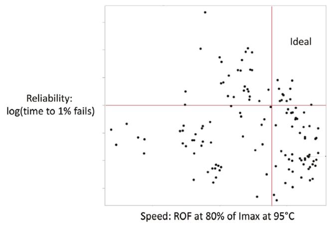
Figure 1. Reliability and speed for a group of different VCSEL designs.
Higher speeds
It is not trivial to produce 28G VCSELs in volume. Therefore, it is a significant challenge to design variants that can provide even higher data rates over a single fibre.
We have had success in this endeavour with a technology known as wavelength-division multiplexing. Since the 1990s, it has been used in the telecom sector, which employs InP-based lasers emitting at 1550 nm.
However, telecom lasers are very different to ours – they emit in single mode and transmit over singlemode fibre; whereas the output from 850 nm datacom VCSELs is multimode. Due to this key difference in modal output, at 850 nm the wavelength separation in a multiplexed link needs to be large enough to prevent optical crosstalk and keep mux and de-mux technology cost effective.
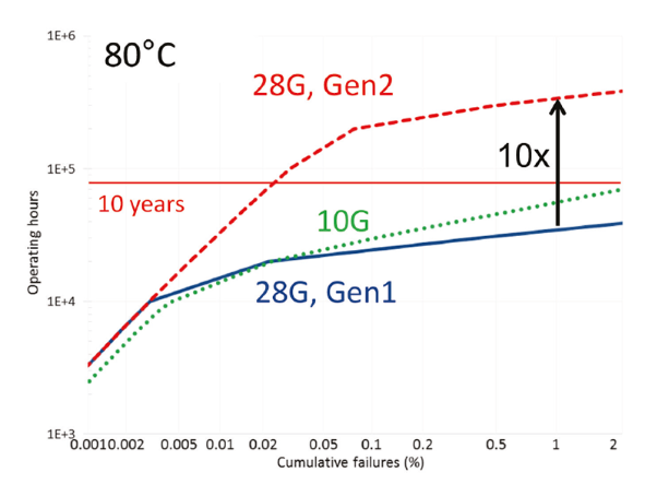
Figure 2. Time-to-failure for Finisar’s Gen 1 and 2 28G and 10G VCSELs operating continuously at 80°C and worst-case bias current of 8 mA for singlets. Ten years of operation is indicated
Grid standardization work is ongoing for shortwave wavelength division multiplexing. Currently, the most common scheme is to use four wavelengths: 850 nm, 880 nm, 910 nm, and 940 nm. Today’s multimode fibre is optimised for 850 nm – and if wavelengths are used that are far from this, modal dispersion will be high and limit the transmission distance of the signal. Due to this, efforts are underway by the like of OFS and Prysmian to develop wideband multi-mode fibre. This technology could create an eight-channel wavelength grid, using additional channels at 970 nm, 1000 nm, 1030 nm, and 1060 nm.
Our 28 G VCSELs for shortwave wavelength-divisionmultiplexing are designed to work over standard multi-mode fibre and deliver a performance that is on par with our 850 nm 28G VCSELs. Thanks to this, our technology can be used to upgrade the transceiver module and increase data rates over existing fibre infrastructure. Options include a ten-fold upgrade to the speed of existing 10G links to 100G, an approach we demonstrated in 2015 at ECOC (see Figure 6).
An alternative approach to increasing speed, which requires only minor changes to existing 28G VCSEL technology, is to change the modulation format for the data that is transmitted. Increasing the number of signaling levels from two to four doubles the amount of information that can be encoded on each symbol. Consequently, the data rate can double while maintaining the same symbol rate, enabling a single channel to support 56 Gbit/s, rather than 28 Gbit/s. This modulation format is called four-level pulsed amplitude modulation.
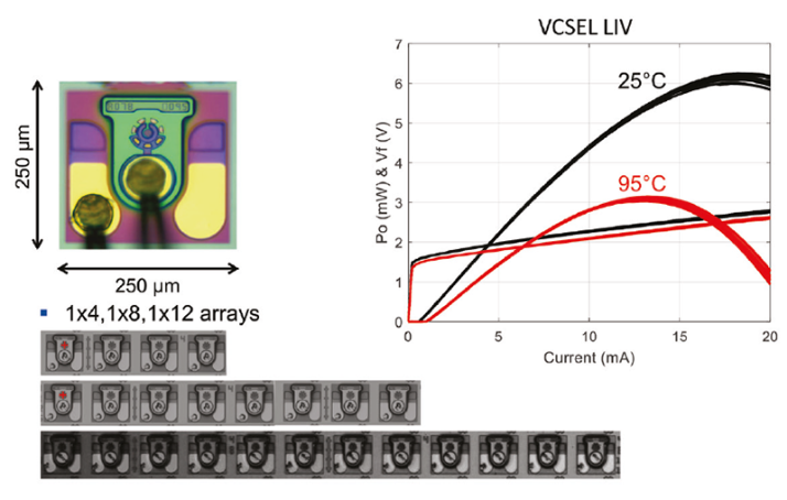
Figure 3. 28G VCSEL singlet and arrays and typical 28G VCSEL light-currentvoltage plots at 25°C and 95°C.
As all engineers know, there is no such thing as a free lunch. Increasing the number of data levels to detect increases the penalties associated with intersymbol interference and signal noise. The ISI penalty translates to a slightly higher requirement for the VCSEL modulation bandwidth, but this may be met by reducing the size of the aperture (see Figure 7). Reliability then takes a hit, but it is still more than adequate, thanks to the enhanced reliability of our Gen 2 VCSEL material. Time to 1 percent failure for continuous operation of individual elements exceeds ten years.
For transmission with conventional, two-level pulsed amplitude modulation, the relative intensity noise is specified as -131 dB/Hz in both the IEEE and ANSI standards. Moving to multi-level signalling shifts this requirement to -138 dB/Hz, and could limit the yield for the standard 28G VCSEL.
To be able to screen for relative intensity noise, and quickly validate design tweaks that could improve this key figure of merit, we introduced an additional production test system. This enabled relative intensity noise measurements on 100 percent of die on the wafer. Thanks to the insight offered by this test system, we could then identify a path to modifying the design of the VCSEL to improve its relative intensity noise (see Figure 8 for the results of this effort). To showcase our success, we provided a live demonstration of our VCSEL running error-free at 56 Gbit/s at OFC 2017 (see Figure 9).
Even faster data transmission rates can be realised by combining four-level pulsed amplitude modulation with shortwave wavelength-division multiplexing. Working in partnership with engineers at Georgia Institute of Technology, we have used this approach to boost the bit-rate per channel to 107 Gbit/s, and ultimately provide an aggregate bit-rate of more than 400 Gbit/s over a single fibre. This accomplishment, demonstrated at OFC 2017, involved a bit-error-rate for all channels in the range of 10-4 – a value that is low enough to enable use with forward-error correction.
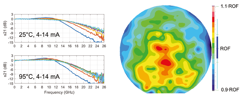
Figure 4. Typical 28G VCSEL modulation response at 25°C and 95°C and map showing the variation in relaxation oscillation frequency (ROF) across a 4-inch wafer.
Low latency applications
Our technology for delivering data at 50G over multimode fibre could be used for Ethernet and Infiniband. 50G data transmission appears on both roadmaps, which differ slightly: for Ethernet, fourlevel pulsed amplitude modulation must be used with forward-error correction, while the latter technology is optional with Infiniband.
A major downside of forward-error correction is that it adds latency to the transmission. This is unacceptable in some applications, such as high-performance computing. For four-level pulsed amplitude modulation, error-free low latency transmission is challenging at 50G, due to a significant penalty associated with the signal-to-noise ratio. What’s more, four-level pulsed amplitude modulation is less power efficient than the more conventional two-level format. Due to these issues, two-level pulsed amplitude modulation is preferred in low latency applications. This is driving efforts to extend the capability of existing 28G designs.
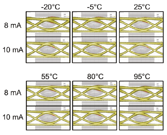
Figure 5. Eye diagrams for a typical 28G VCSEL at 28 Gbit/s at different temperatures and currents.
To ensure error-free transmission at 56 Gbit/s with twolevel pulsed amplitude modulation while maintaining the link budget, the modulation bandwidth must exceed 30 GHz. Several groups, including Chalmers University of Technology, have demonstrated these bandwidths in laboratory environments with VCSELs that feature an optimised small aperture. However, reducing the aperture size to these dimensions is challenging – and doing so in a production line, while ensuring high reliability, is particularly difficult.
Another possibility for squeezing more out of the existing technology is to implement electronic equalization at the transmitter and receiver end. This mitigates the bandwidth limits of the link. Using our VCSELs, and also those from Chalmers University of Technology, IBM has demonstrated this type of link, and produced error-free transmission with two-level pulsed amplitude modulation signalling at bit-rates of 50 Gbit/s and beyond (see Figure 10 for an example). However, there are drawbacks to this approach, such as increases in transceiver complexity and power consumption.
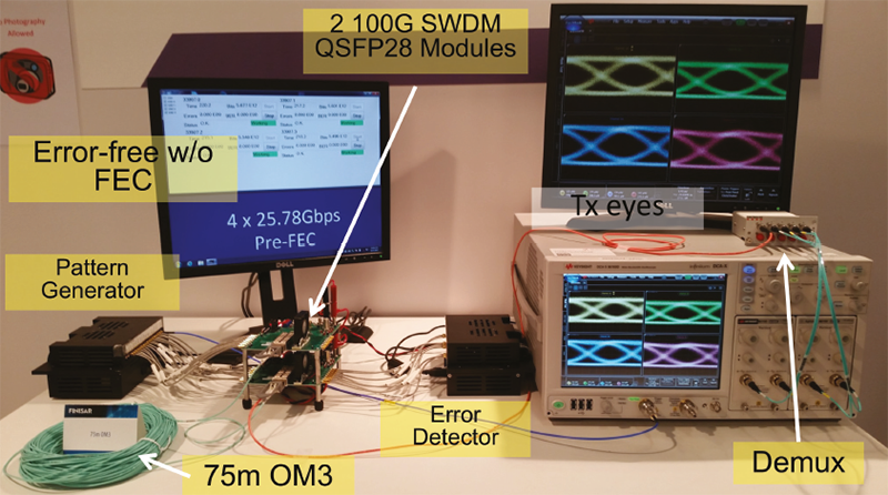
Figure 6. Live demo at ECOC 2015 of a four-channel shortwave wavelengthdivisionmultiplexing VCSEL delivering error-free transmission at 4 x 25Gbit/s over a single 75 m long multi-mode fibre. Note that forward error correction is not used.
With demand for increasing bandwidth showing no sign of abating, a great deal of effort is being devoted to optimising the modulation response of the VCSEL. A few more gigahertz may be squeezed out of this device through incremental improvements in the likes of carrier and optical confinement, differential gain, internal absorption and electrical parasitics. However, it is not clear if this could spur the speed to 30 GHz and beyond. Therefore, efforts are underway on implementing less conventional approaches that promise to bypass the intrinsic speed limit of the VCSEL, set by the finite differential gain and the damping of the laser.
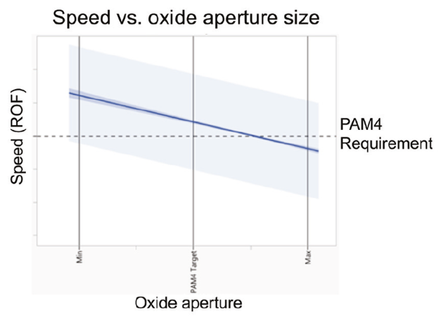
Figure 7. Speed as function of 28G VCSEL aperture size for a group of production wafers.
One potential route to success is to integrate an electro-optic modulator with the VCSEL. This modulator could, in principle, bypass the intrinsic speed limit of the VCSEL, by only being limited by the ‘RC’ time constant of the modulator. Vertical integration of the modulator has been attempted by groups that include a team at TU Berlin, while lateral integration has been pursued by researchers at Tokyo Institute of Technology.
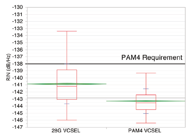
Figure 8. Mean diamond box plots of the relative intensity noise (RIN) of different VCSEL designs. Measurements are made on a production RIN tester. The 56G PAM4 (four-level pulsed amplitude modulation) VCSEL, which is indicated, has a part yield that’s better than 95 percent for the RIN requirement.
Neither of these options is easy. Challenges include: increased epitaxial complexity; modulating the device without affecting the cavity photon density; and keeping electrical parasitics small, so that high speeds may be realised alongside a sufficiently high output power and extinction ratio.
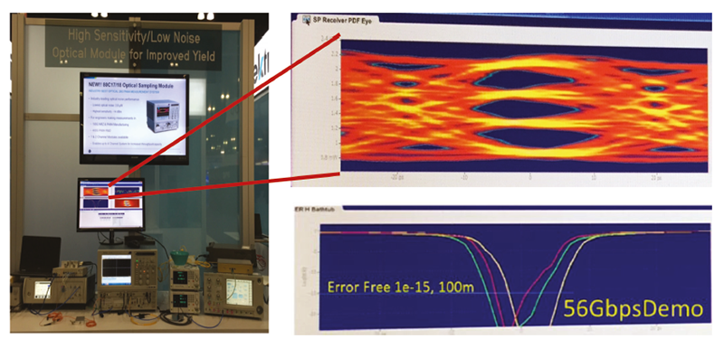
Figure 9. A live demo of 56 Gbit/s PAM4 (fourlevel pulsed amplitude modulation), given at OFC 2017.
An alternative approach to enhancing the modulation response is to exploit optical feedback through the so-called detuned-loading or photon-photon resonance. We have had success with this, enhancing the modulation bandwidth in edge-emitting lasers beyond 50 GHz. This has led to error-free transmission at more than 50 Gbit/s, using two-level pulsed amplitude modulation (see, for example, our paper from OFC 2016). Optical feedback effects have also been exploited to enhance speed in VCSELs made by groups at Tokyo Institute of Technology, Fuji Xerox, and the University of Illinois at Urbana Champaign. Those VCSELs are producing promising small-signal modulation speeds, but there is a lack of large-signal data transmission results.
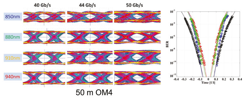
Figure 10. Eye diagrams for the shortwave wavelength-division-multiplexing VCSEL channels at different bit-rates, along with bathtub curves at 50 Gbit/s, showing error-free transmission using IBM’s BiCMOS drivers and equalization.
We are also pursuing alternative approaches to reaching higher VCSEL speeds. Early results are encouraging, with VCSELs producing an optical modulation bandwidth greater than 30 GHz (see Figure 11). We are now evaluating and analysing the commercial viability of these devices.
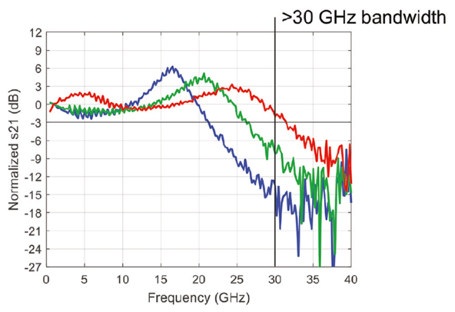
Figure 11.Normalized modulation response for a candidate VCSEL for 56G operation, using two-level pulsed amplitude modulation.
Users of SiC devices are starting to benefit from a dedicated lab that provides new insights into the characteristics of SiC power devices. By Aly Mashaly from Rohm Semiconductor
Power Semiconductors are cropping up everywhere. They are being deployed in electric vehicles, charging station infrastructure, solar and wind power plants, and industrial machinery.
One of the key requirements for every power device is that it complies with energy efficiency requirements. To ensure that this is the case, the devices – either forms of diodes, transistors or thyristors – are tested and validated at an early stage of development. This testing is evolving, due to the introduction of everhigher switching rates and operating voltages.
The cnages in the switching rates and operating voltages are playing into the hands of SiC devices, which have the upper hand over silicon incumbents. But the faster switching speed has a challenging consequence: a need for specialised testing. To meet this requirement, dedicated test setups are needed to deliver the precise results that are desperately wanted by those that will design products with these devices.
At Rohm Semiconductor, a market leader in SiC technology, we are striving to provide our customers with the best possible support. To that end, earlier this year we opened a 300 m2 ‘Power Lab’ for the analysis of power devices and systems. This facility is located in Germany, at our European Headquarters in Willich-Münchheide, which is just outside Düsseldorf.
The primary purpose of our lab is to help our customers realise the benefits of power devices, and to go on and make great products that generate great sales. Our lab can be used to test devices, or systems such as inverters, which may be formed from SiC devices, or a mix of SiC and silicon. One option for our customers is to tell us what testing they require, and trust our engineers to make these measurements – alternatively, they can visit our lab, and use our specialised equipment to carry out the tests themselves.
We know that the engineers that purchase our power devices, or consider doing so, face many challenges. These engineers are under pressure to comply with the current trend of making products that combine higher efficiency with higher power density and higher reliability. Succeeding in this endeavour is not easy, because it brings its own challenges, such as thermal management. Making the engineer’s task even harder, system requirements are getting ever more complex, while the time to complete the project is limited, and it must be accomplished within its financial constraints.
Given this scenario, it’s hardly surprising that many of today’s system engineers are choosing the easiest way to design their circuits. Going into their products are tried-and-tested reference designs, likely to be dominated by silicon chips.
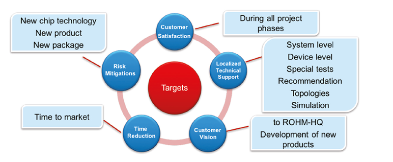
Figure 1. ROHM Semiconductor’s new “Power Lab” aims to provide customers with the best technical support at an application level when using wide bandgap power devices.
To help these engineers make the switch to SiC devices, they need data for these wide bandgap power devices that demonstrates how to use them in applications in the best possible way. Ideally, this data will aid the building of products that are reliable, low in cost, and easy to use.
Makers of SiC power devices, including ourselves, must do more to help every engineer that is considering to use these chips. It is not enough to simply provide a datasheet for each device and system requirements for each power board. Why? Because, for example, the operating points of the final application are not always covered in the datasheets.
Simply adding a few more numbers to the datasheet is not going to address this issue. The reality is that power semiconductors serve in many different application fields, where they operate in many different manners. Depending on the application, there can be different loads, such as DC motors, AC motors and batteries; and there can be different power sources, such as batteries and the grid. The products that are built with these diodes and transistors could be deployed all over the world, so they need to operate over a range of temperatures and humidity levels – and if they are powered by the grid, they need to be compatible with the local power supply.
What the engineers that are building products with power electronics need is technical support. And that is what we can now give them, by making the specific measurements that they need in our new Power Lab. Here, we can test discrete devices under a range of conditions, and also power systems, which may contain a mixture of silicon and SiC components.
The Power Lab project began with a detailed, structured-use case analysis. Throughout the whole project, it was crucial to never lose focus of either the target application or the customers. While making these the priorities, time is taken into account, along with internal and local safety standards.
All these projects benefit from drawing on the great experience of our team, which has many years of experience in power electronic applications and the testing of power devices. The project’s success also results from modern measurement techniques and equipment.
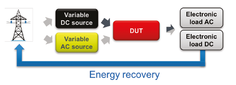
Figure 2. The power test bench feeds energy back into the grid to minimize the energy consumption.
Creating the Power Lab
When we started to plan for the build of our power lab, we had to evaluate the relative importance of many factors. We decided that when we were putting together test benches with state-of-the-art and advanced technologies, emphasis had to be on safety and the quality of the equipment. We also placed a premium on flexibility of usage.
We decided to deploy a flexible, modular design for our test set-ups, because this enables us to provide fast, high-quality support to our customers. What’s more, this gave our Power Lab the capability to be prepared for future products and market trends.
It didn’t take us long to realise that our Power Lab would not be an off-the-shelf product. After specifying the test benches, we had to decide whether we should design the Power Lab ourselves, or hand this task over to an experienced design house. Following careful consideration, we decided on the former. Taking this approach would help to ensure the high quality and reliability of the test benches – and by keeping our know-how in-house, we could ensure that any future modifications would be easier.
After several months of construction, we started using our Power Lab in late 2017 (the official opening followed in 2018). In this purpose-built facility, we can carry out tests on SiC MOSFET transistors, SiC diodes, IGBTs, silicon power MOSFETs and gate drivers at DC voltages of up to 8000 V. These measurements can be carried out in a designated high-voltage room, equipped with several test benches.
The primary purpose of our test benches is the electrical characterization of MOSFETs and IGBTs. For these devices, we can use voltages up to 1500 V to measure switching times and losses, conduction losses and short circuit behaviour. Thanks to the high flexibility of our modular approach, testing is possible on various packages, such as THD, SMD, modules and customer boards.
In our lab, we have converters that can accommodate every configuration of AC and DC input and output, and put devices through their paces under realworld conditions of up to 15 kVA. Our test bench features an AC power supply (grid emulator) and various electronic loads, both in AC and DC form, with maximum voltages under test of 1500 V DC and 400 V AC. In addition, we can provide high-precision measurements of efficiency and losses. And to trim the carbon footprint of our facility, a regenerative function allows us to feed part of the energy that we use back into the grid, reducing our total energy consumption during testing.
The thermal analysis of modules, discrete devices, electronic boards, and even complete power electronics systems can be undertaken on our calorimetric test bench. It features continuous power supplies with a high current level, and a climatic chamber that can range in temperatures from -40 °C to 180 °C and provide humidity levels from 10 percent to 98 percent.
On another test bench, engineers can evaluate the isolation of in-house developed circuits, PCBs and reference designs. For these studies, the power supply enables a programmable output ramp up to 6 kV and 10 mA. For example, this setup can test the clearance and creepage distances of isolated gate driver boards.
Following the opening of our Power Lab, we are strengthening our relationship with our customers, who appreciate our insightful, prompt support at the application level. As well as providing this service, we are starting to undertake our own internal projects. Our aim with these test boards is to put power devices through their paces at the system level. Evaluations will be from a customer perspective. The results of these efforts will soon be published, in the form of application notes and reference designs.
Wafer level integration of InGaAs HEMTs and silicon CMOS can create millimetre-wave circuits with a small footprint, low cost and high performance by Sachin Yadav, Sang Xuan Nguyen, Fayyaz Singaporewala, Kenneth Lee, Eugene Fitzgerald and Xiao Gong from the Singapore-MIT Alliance for research and technology – low energy electronic systems
Since the introduction of the integrated circuit in 1959, silicon has dominated the semiconductor industry. In the form of silicon CMOS, it has advanced at a rapid pace to offer an unparalleled device integration density.
However, silicon cannot do everything. In the highfrequency domain, devices made from this material are inferior to those formed from the likes of GaAs, GaN and InP – all those alternatives offer higher powers, lower noise and superior linearity. Due to this, the trend in modern communication devices is to bring together high-speed III-V devices and high-density silicon-CMOS on the same circuit board.
Until recently, this integration has taken place at either the board or the packaging level. That’s not ideal, though, as it leads to a large circuit footprint, large interconnect losses, and high cost.
A far better option is wafer-level integration of different material systems. This approach opens up a plethora of new opportunities for future communication devices. As can be the case for a silicon-only RF technology, monolithic heterogeneous integration promises lower costs, reduced interconnect power consumption, superior circuit performance, a smaller chip footprint, fewer packages at the board level, and more room for circuit innovation for millimetre-wave communication applications, such as 5G mobile and wireless.
The superior performance that comes from monolithic integration partially results from the opportunity to position silicon and III-V devices very close together – they can be separated by a few microns, and sometimes even less. Systems that can be realized in this manner include a transceiver based on the hybrid monolithic integration of silicon and III-Vs (see Figure 1). This system can combine an RF front-end formed with high-performance III-Vs, or a combination of III-V and silicon-CMOS devices; with a digital baseband in highly integrated silicon-CMOS technology. It’s a marriage that brings out the best in both III-V and silicon.

Figure 1. Hybrid transceiver systems can exploit the advantages of III-V and silicon-CMOS technologies. Using this approach, high-performance amplifiers, filters, and converters can be designed using III-V technologies, while the control and digital circuitry can be designed using silicon-CMOS. In addition, hybrid sub-circuits, such as ADC (analogue-to-digital converters) and DAC (digital-to-analogue converters), can be implemented using a combination of III-V and silicon-CMOS devices.
Which III-V?
Several III-V technologies can be used to produce power and low-noise solid-state amplifier technologies at millimetre-wave frequencies – that is, those that span 30 GHz to 300 GHz. Out of these options, InGaAs HEMTs and HBTs offer the most balanced noise and power performance for 5G applications (see Figure 2(a) for on-chip output powers of various microwave, millimetre-wave, and sub-millimetre-wave power amplifiers).

Figure 2. (a) Plotting the output power as a function of frequency for various on-chip III-V power amplifiers reveals that for operating frequencies less than 100 GHz, GaN-based power amplifiers provide a superior performance compared with that of other solid-state technologies. For frequencies above 100 GHz, InGaAs HEMTs and InP HBTs lead to the best power performance. (b) Comparing noise figures at various frequencies for various low-noise amplifiers shows that those based on InGaAs HEMTs provide the best noise performance.
The preference for InGaAs might raise a few eyebrows, given the success of GaN in the RF domain. However, while GaN-based MMICs exhibit the best power output among the solid-state device technologies, the GaN PA is compromised by a high operating voltage, due to the large knee-voltage of the GaN HEMT.
If a hybrid III-V and silicon technology is to create a device with tremendous sales, it will have to target a high-volume product that already uses silicon. In the wireless space, such volumes are already achieved in mobile devices, such as handsets. Handsets, however, operate at voltage ranges where GaN loses its primary advantage.
For frequencies exceeding 100 GHz, the best PA performances come from InGaAs HEMTs and InP HBTs. Of these two, InGaAs HEMTs have lower noise figures, making them the premier choice for low-noise amplifiers operating in this frequency domain. The upper hand stems from the record high transconductance, electron mobility, and cut-off frequencies of InGaAs HEMTs – and bandgap engineering enables these devices to span a frequency range that extends all the way from a few gigahertz up to 1 THz. So these devices are versatile, while their combination of medium output powers and low noise figures make the InGaAs HEMT-based amplifier the most suitable candidate for applications such as 5G mobile.
Integrating InGaAs and silicon
At the Singapore-MIT Alliance for Research and Technology Low Energy Electronic Systems (SMART-LEES) we are integrating InGaAs MOS-HEMTs with silicon CMOS, using 200 mm silicon wafers (see Figure 3).

Figure 3. At SMART-LEES, heterogeneous integration involves the use of InGaAs HEMTs and silicon-CMOS. First, the silicon-CMOS front-end is fabricated and transferred to InGaAs-on-silicon wafers. After this, InGaAs HEMTs are fabricated in etched windows. Finally, at a CMOS foundry, back-end-of-line processing creates interconnects between silicon-CMOS and InGaAs HEMTs.
One of the merits of this approach is that by using large-diameter wafers, we can address the ever increasing demand for such technologies. Additional attributes are that the integration can employ existing, mature silicon multi-layer interconnects; and hybrid circuits can be formed, by combining p-type silicon transistors with n-type InGaAs transistors. The separation between these two different types of devices may be as small as just a few microns.
The MOS HEMT is a lesser known device than the commercially available Schottky-gate HEMT. But in our circuits, we believe it’s a better choice. In recent years, InGaAs MOS devices and ohmic contacts have received significant attention in the research community, due to successes that include a record transconductance for InGaAs quantum-well MOSFETs among all III-V FETs. Another feature of the MOS HEMT is that it can contain a high-κ gate oxide, which can slash the gate leakage current compared with that of the Schottky gate HEMT. This is most welcome, because it opens the door to more aggressive device scaling and higher device density.
We process our silicon CMOS and InGaAs front-end devices sequentially in a CMOS-flow (see “Uniting CMOS and InGaAs front-end devices”). Our process includes a wafer bonding step (see Figure 4).

Figure 4. (a) Photograph showing the bonded patterned SOI and InGaAson-silicon substrates. (b) A cross-sectional transmission electron microscopy image of the bonded SOI (patterned) and InGaAson-silicon substrates.
A key advantage of our approach is that it allows a decoupling of thermal budgets that are associated with front-end-of-line processes for silicon and InGaAs. Thanks to this, the high temperatures of 600 °C or more, which are needed for the epitaxial growth of the III-V device layers, are kept away from the devices formed on the silicon wafer during front-end-of-line processing. What’s more, our approach avoids degradation that could be caused by exposing the InGaAs MOS-HEMTs to temperatures associated with the front-end-of-line processing steps used for silicon CMOS.
Growth of our InGaAs HEMTs is carried out in an Aixtron Crius MOCVD reactor, using 725 μm-thick silicon (001) substrates with a 6° offcut and a diameter of 200 mm. To balance the device cut-off frequency, which is related to electron mobility, with the breakdown voltage that is related to the energy bandgap, we use an indium composition in our channel of 30 percent. Buffer layers address the large lattice mismatch between In0.30Ga0.70As and silicon – it is 6.3 percent (see Figure 5 for details of the epistructure of our HEMT).

Figure 5. At SMART-LEES, InGaAs HEMT structures are grown on 200 mm silicon substrates using an Aixtron Crius MOCVD reactor.
To realise high-quality device layers, we have improved the material uniformity of our epitaxial structures, while decreasing the threading dislocation density, wafer bow and surface roughness. Using a high growth temperature of 630 °C and a relatively thick InAlAs graded buffer – it is about 1.5 μmthick – we have produced material with a threading dislocation density of 1±0.3 × 107 cm-2, according to plane-view transmission electron microscopy. Based on results of 50 growth runs, wafers are slightly concave, with a bow of just 39±4 μm. Variations in material composition across the wafer are very small, thanks to a difference in temperature of just 5 °C from the centre of the wafer to its edge, and uniform gas flows provided by the showerhead configuration of the MOCVD tool.
Uniting CMOS and InGaAs front-end devices
Using the integration approach adopted by the engineers working in the Low Energy Electronic Systems group at Singapore, CMOS and InGaAs front-end devices are processed sequentially in a CMOS-flow. Fabrication involves the following steps:
Atomic force microscopy reveals a root-mean-square surface roughness for the top n+-InGaAs cap layer of 5.7 nm (see Figure 6). Note that this value is higher than that for MBE-grown HEMTs, due to the higher growth temperature, which trades a superior material quality for a slight increase in cross-hatch roughness over large length scales.

Figure 6. (a) Atomic force microscopy scan of the top InGaAs surface for a scan area of 30 μm by 30 μm. The RMS roughness is about 5.7 nm. (b) Hall mobility data from various samples with different δ-doping species and indium compositions in the InxGa1-xAs channel. By optimizing the δ-doping, a μHall of more than 5000 cm2 V-1 s-1 can be realised in both tellurium and silicon δ-doped samples.
By varying the δ-doping concentrations and species, we realise mobilities in the In0.30Ga0.70As channel of 5000-6500 cm2 V-1 s-1, according to Hall measurements. The use of graded buffer technology allows us to vary the indium concentration in the thin channel layer by around 20 percent, without penalizing the material quality. This has enabled us to produce In0.40Ga0.60As channel devices with Hall mobilities exceeding 7000 cm2 V-1 s-1. Being able to tune the composition is highly desirable, because it enables us to balance our device’s breakdown voltage and cut-off frequency.
The performance of our InGaAs MOS-HEMTs can now approach that of GaAs pHEMTs and mHEMTs, following optimisation of the gate-stack modules and the ohmic contact, which is based on tungsten and molybdenum. Benchmarking effective mobility for our MOS-HEMTs against that of InGaAs MOSFETs with surface and buried channels reveals that our device has one of the best values for a transistor formed on silicon, thanks to its optimised energy barrier and gate-stack layers (see Figure 7(a)). This mobility, combined with a source resistance as low as 300 W×mm, gives a high transconductance of 560 mS/mm for a device with channel length of 0.33 mm (see Figure 7 (b)). The current gain cut-off frequency for our devices is 60 GHz, extracted for transistors with 150 nm gate lengths.

Figure 7. (a) Reported effective mobility (μeff) as a function of effective oxide thickness (EOT) at sheet electron density (Ns) of 3 ×1012 cm-2 for InxGa1-xAs (x ≤0.53) channel MOSFETs fabricated on silicon, GaAs, and InP substrates. The μeff in the MOS-HEMT produced at LEES is among the highest reported for InGaAs MOSFETs on large area silicon substrates. Note that triangles represent buried-channel MOSFETs and squares surface-channel MOSFETs. (b) Peak transconductance (Gm) as a function of channel length (LCH) for GaAs mHEMTs, pHEMTs, and LEES’ MOS-HEMTs on silicon. As a result of high III-V material quality, LEES’ MOS-HEMTs on silicon can achieve a transconductance that approaches that of GaAs HEMTs on native GaAs substrates at similar channel length. Note that mHEMTs and pHEMTs refer to metamorphic and pseudomorphic HEMTs, respectively.
We are now working on optimizing the millimetrewave power and noise performance of our devices, and developing hybrid circuit technologies for future communication systems.

The authors would like to acknowledge the support of the National Research Foundation of Singapore through the SMART’s LEES IRG research program, as well as the current and former members of the LEES team including Annie Kumar, David Kohen, Saeid Masudy-Panah, Kwang Hong Lee, Viet Cuong Nguyen, Cheng Yeow Ng, Chuan Seng Tan, Dimitri A. Antoniadis, Yee-Chia Yeo, and Soo Jin Chua who have contributed to the results reviewed in this article.
Further reading
http://smart.mit.edu/research/lees/lees.html
http://www.circuit-innovation.org/
http://www.compoundsemiconductor.net/article/98881-building-theics-of-the-future.html
https://compoundsemiconductor.net/article/100488-adding-colour-tofuture-silicon-ics.html
S Yadav et al. IEDM Tech. Dig., 421-424 (2017)
EA Fitzgerald et al. ECS Transactions 75 439 (2016)
D Kohen et al. AIP Advances 6 085106 (2016)
KH Lee et al. AIP Advances 6 025028 (2016)
Stretching the emission of semi-polar LEDs down to 270 nm with growth on the r-plane of AlN
Researchers at Kyoto University, Japan, are claiming to have created the first semi-polar LED that emits below 300 nm.
Producing emission that is below 300 nm is an important breakthrough, because it can be used for the sterilization and purification of water and air. For several years, conventional LEDs have been capable of emission below 300 nm. However, semipolar variants have more promise, because this orientation has weaker internal electric fields, leading to a higher likelihood of radiative recombination.
“Although the external quantum efficiency of the present semi-polar LED is low, we believe that it can exceed that of polar LEDs,” explains team spokesman Yoichi Kawakami. According to him, developing semipolar deep UV LEDs is far from easy, because there are no established growth conditions.
“It took more than one year to find growth conditions available for semi-polar LED growth,” says Kawakami.
He and his co-workers produced their semi-polar LEDs on r-plane AlN substrates, sliced from AlN bulk crystals with a diameter of about 1 cm. This foundation has relatively low levels of impurities of silicon, carbon and oxygen, enabling AlN substrates with a thickness of 450 μm to have a transmittance of more than 50 percent at wavelengths between 250 nm and 280 nm.
AlN has a surface layer of aluminium hydroxide. To remove this, the engineers wet-etched the surface for 10 minutes at 90 °C with a mixture of sulphuric acid and phosphoric acid.
After this, the researchers loaded the substrates into an MOCVD chamber and deposited a stack of epilayers at a growth pressure of 200 Torr. Applying growth conditions that had been established by scrutinising layers grown at different rates, temperatures and V/III ratios, the team produced LED structures that featured: an active region with three, 2 nm-thick AlGaN quantum wells separated with 5 nmthick AlGaN barriers; a 1 nm-thick, undoped electronblocking layer; and two 7.5 nm-thick AlGaN layers, next to one another. That pair of layers, which have different compositions, are designed to improve hole injection into the active region.
Photolithography and reactive-ion etching created 500 μm by 500 μm LED mesas from the epiwafers. The addition of n and p electrodes, formed from stacks of Ti/Al/Ti/Au and Ni/Au, respectively, completed device fabrication.
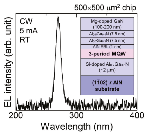
The semipolar r-plane has aided the fabrication of UV LEDs emitting below 300 nm.
The device has a turn-on voltage of about 8 V, according to plots of current as a function of voltage. This value, far higher than the theoretically expected 5.1 V, is attributed to the low conductivity of the p-type GaN layer and insufficient hole injection from this layer to the quantum wells.
The team estimated the output power of their devices by placing a silicon photodiode beneath the substrate. This approach produced a value of 1.6 μW at 10 mA, compared to 10.4 μW for the control, a c-plane device, grown side by side on an AlN-on-sapphire template.
The researchers also measured the electroluminescence intensity produced by their semi-polar device. It peaked at around 5 mA.
Kawakami believes that the performance of their semipolar device can be improved by refining the growth conditions.
“The first thing we have to examine in a future study is further optimization of semi-polar quantum-well growth,” says Kawakami. Efforts will also be directed at improving the growth of p-type AlGaN. This could lead to greater suppression of electron overflow, and ultimately a hike in current injection efficiency.
Reference
R. Akaike et al. Appl. Phys Express 11 061001 (2018)
GaN VCSELs can now be equipped with tunnel junctions that are grown by MOCVD
Attributes that include a circular emission profile, a small size and a high modulation bandwidth make the GaN VCSEL a very promising device for visible light communication, optical sensors, displays and atomic clocks.
Unfortunately, the output power of today’s devices are incredibly low, and their fabrication notoriously difficult – but for the latter issue, an important step has just been taken by a team from the University of California, Santa Barbara (UCSB). This group is claiming to be the first to use just MOCVD togrow a GaN VCSEL structure that incorporates a tunnel-junction.
“Most GaN-based VCSELs have used ITO for current spreading because efficient tunnel-junction contacts are hard to achieve,” explains UCSB spokesman SeungGuen Lee. However, ITO has a high absorption loss, leading to higher threshold currents and a lower light output.
Tunnel-junctions address this, and back in 2015 the team reported success with this approach. However, they did so by using MBE, an approach that Lee claims to be “not applicable in industry.”
In the latest work they fix this, using MOCVD to grow an 408 nm source that sports a tunnel-junction and produces a maximum output power of more than 300 μW. Its threshold voltage is almost 8 V.
“One drawback of tunnel-junction contacts is the extra voltage,” admits Lee. Consequently, using these junctions in LEDs is controversial, because they trade a lower wall-plug efficiency for higher light extraction. But with the VCSEL, the decision is clear cut: “The improvement is much greater than the extra voltage – and the extra voltage will keep decreasing as we optimize more.”
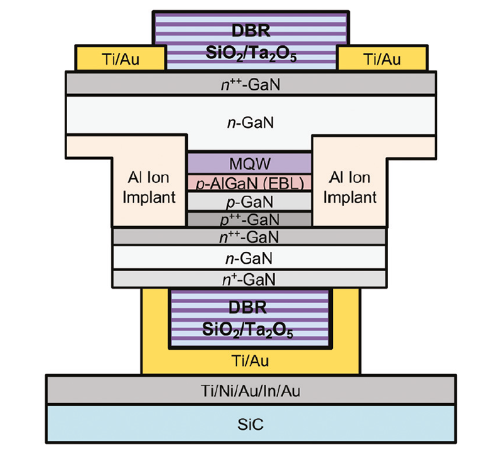
The GaN flipchip VCSEL made by the team at the University of California, Santa Barbara, features dual dielectric distributed Bragg reflectors and a MOCVDgrown tunneljunction contact.
To develop a process for activating the p-type GaN in the MOCVD-grown tunnel junction, Lee and co-workers experimented with LED-based test structures. They were produced with two growth steps: the first formed the LED structure, ending with p-type GaN; and the second added the n-type GaN to form the tunnel junction. Comparing different surface treatments and activation conditions revealed that the best results were obtained by exposing the surface in buffered hydrofluoric acid, and then activating the p-type GaN with in-situ heating.
The team used the knowledge gained from their experiments to fabricate their VCSELs. They began by growing the main epitaxial structure and then forming the current aperture with a mesa etch and aluminium ion implantation. Fabrication of the tunnel junction followed, prior to etching and deposition of a 17 period distributed Bragg reflector, formed from the pairing of Ta2O5 and SiO2. Metal contacts were then added, before flip-chip bonding the structure to a metalcoated SiC substrate and removing the GaN substrate by etching. The final steps involved the addition of an n-type contact and a 13-period distributed Bragg reflector, again made from Ta2O5 and SiO2.
It is very expensive to produce these VCSELs, because the growth of the epistructure is undertaken on m-plane GaN substrates. “It has been proposed to reuse the GaN substrate after flip-chip bonding and substrate removal,” says Lee, but much more work is required before this step could be used in industry.
Room-temperature measurements on the team’s GaN VCSEL, using 300 ns pulses and a 0.3 percent duty cycle, revealed a threshold current density of 10 kA cm-2, and a threshold voltage of 7.8 V. At 12 V, the device produced its peak output power of 319 μW.
The team are now developing designs that provide current confinement with buried tunnel junctions, rather than ion implantation. “Aluminium ion implantation makes gallium nitride optically absorbing, which increases internal loss,” explains Lee. Work is in its early stage, but Lee says that initial results are very promising.
Reference
S.G. Lee et al. Appl. Phys. Express 11 062703 (2018)
Spin-coating a polymer into an array of nanowires creates a flexible, optically pumped laser
Researchers at the University of Tokyo are claiming to have produced the first nanowire-based lasers on flexible substrates.
Their efforts will aid the development of mechanically flexible modules that can provide a coherent light source in windows, papers, skins, contact lenses, and even inside the human body, where they promise to enable human-interactive optoelectronic devices.
The Japanese team’s breakthrough involves the creation of an optically pumped laser in a single nanowire cavity, formed from quantum dots embedded on flexible substrates. To form such a structure, spin-casting and curing steps were used to transfer the nanowire cavity into membranes of the polymer PDMS.
Fabrication began by loading patterned GaAs substrates into an MOCVD chamber and growing wires, consisting of a GaAs core, followed by a 50-layer stack of In0.2Ga0.8As nanowire quantum dots and GaAs/Al0.1Ga0.9As core-shell-cap layers. The patterned substrate had been formed by depositing a 10 nm-thick layer of SiO2 on GaAs, and then using electron-beam lithography and reactive-ion etching to create an array of holes, 30 nm in diameter and separated by a 500 nm-pitch.
The next step involved mixing the PDMS with a curing agent in the ratio 10:1, and spin casting this on the sample for 60 s. Repeating this process ensured that the thickness of the membrane is sufficiently large – it is in excess of 100 μm, according to cross-sectional, scanning electron microscopy.
After leaving for several hours, to ensure that the polymer in completely integrated within the grooves, the researchers cured this sample for an hour at 120 °C. Finally, they gently peeled the cured PDMS membrane from the substrate.
This membrane, which is transparent and easy to fold, has been scrutinised with several forms of microscopy. Scanning electron microscopy reveals that the nanowires are typically 4 μm high, and have a diameter of 300 nm, while cross-sectional scanning tunneling electron microscopy shows that the dots are, on average, less than 40 nm in diameter and shorter than 7 nm.
Placing the sample in a cryostat, cooling it to 10K, and pumping the dots with a 780 nm Ti:sapphire laser produces a luminescence peak at 1.41 eV, associated with spontaneous emission from the ground state of the dots. Under weak pumping, this peak has a full-width at half-maximum of 60 meV, due to inhommogeneous broadening associated with fluctuations in the dimensions of the dots. As the fluence increases, the photoluminescence peak shifts to higher energies, due to state filling within the dots.
Additional increases in fluence take the lasing spectra from below to above threshold, where emission shifts to 1.425 eV, associated with a high sub-band of the nanowire quantum-dot cavities.
The team notes that this emission stems from only a fraction of the nanowire quantum-dot cavities, due to large variations in the dimensions of the wires, the dots and the crystal quality. It is argued that optimisation of the growth conditions could lead to improved size uniformity of the nanowire quantum dots, and ultimately better device performance, including a higher yield of lasers.

One of the potential opportunities for the nanowire quantum dot technology is to enhance the capability of contact lenses
Another of the team’s observations is that the lasing threshold of the devices on the flexible substrate is higher than that for nanowire quantum dot lasers placed horizontally on a SiO2-on-silicon substrate.
The higher threshold is partly attributed to a lower reflectivity at one side of the end facet, due to the lower index at the interface between the nanowire and the PDMS. This leads to a relatively large mirror loss. Another factor behind the high threshold is the low facet quality, stemming from the peeling of the membrane from the substrate.
To address these weaknesses, the researchers advocate adding gold to the top of the cavities prior to spin coating, and optimising the technique used to form their flexible devices.
Reference
J. Tatebayashi et al. Appl. Phys. Express 11 065002 (2018)

