


There is hardly a more exciting place than being on the cusp of advanced technology. This edition examines the needs and frustrations of bringing new devices to market and the many ways that PIC innovators are revolutionizing photonic integration. Mark Andrews, the new PIC editor reports.
Photonic integrated circuits are well on the road to revolutionizing datacom and a host of other optoelectronic applications. While it is exciting and challenging to be at the forefront of technology roaring into life, it can also seem to the engineers and scientists working to satisfy the unique requirements of PIC devices that they are running a marathon, not a sprint.
This edition of PIC Magazine addresses a common theme of PIC International (10-11 April)—in a word: Packaging. While the industry’s PIC leaders are regularly announcing new breakthroughs, advances in speed and efficiency, and progress towards resolving vexing materials or performance challenges, automation, testing and packaging remain key considerations.
Vincent Zeng and two fellow quality engineering managers from Facebook continue a conversation begun at PIC International in an interview detailing the challenges of rolling out 100G CWDM4 transceivers on schedule. Quality issues have dogged the rollout, but Zeng remains optimistic about solving issues by removing as much of the hands-on assembly of PIC devices as possible through greater automation. He also places hope in implementing industry-wide quality assurance practices similar to those that have served the CMOS integrated circuit sector for decades.
Also addressing packaging are the experts at ficonTEC, who have provided an in-depth look at the challenges of combining assembly and test into process tools and back end of line (BEOL) automated systems that will handle the unique requirements of both electrical and optical testing for PIC modules and assemblies, highlighting their work with AIM Photonics, PIXAPP and the Tyndall National Institute.
Debuting in this edition is a contribution from the European Photonics Industry Consortium (EPIC), with articles by EPIC’s Director of Technology and Innovation, Dr. Jose Pozo, profiling LiGenTech and QPOlens. Pozo also provides updates on the organization’s most recent international meetings and future strategic work across Europe and the world. Ana Gonzalez and Pozo also take an in-depth look at combining silicon photonics and VCSELs.
Our cover feature in this edition profiles a relative newcomer to PIC, Pilot Photonics based in Ireland. Pilot’s CEO, Dr. Frank Smyth, details his company’s focus on the potential of comb laser sources to address exciting opportunities across communications networks, Internet of Things (IoT) applications, as well as their suitability in research and commercial space programs. Smyth explains how his unique gain switched combs can bring unparalleled performance to many optoelectronic applications.
Pilot Photonics is making laser comb sources suitable for coherent optical transceivers for the first time. As CEO Frank Smyth explains, the techniques and products his company have developed have the potential to transform photonic integration.

An optical comb source is a laser that produces a spectrum consisting of multiple equidistant frequencies. The huge potential of optical comb lasers was recognised in 2005, when they were the subject of the Nobel Prize for Physics, an accolade reserved for highly disruptive discoveries, efforts and inventions. The prize was awarded to John L. Hall and Theodor W. Hänsch "for their contributions to the development of laser-based precision spectroscopy, including the optical frequency comb technique".
Optical combs have been demonstrated as useful tools to enhance a diverse range of applications including precision spectroscopy, microwave synthesis, frequency metrology, optical clocks, and communications.
At its simplest, an optical comb can be used to replace an array of independent lasers, like those of a wavelength division multiplexed (WDM) communications system. However, it is their more subtle properties; the coherence of the comb lines, and the precision of the frequency spacing between them, that create new possibilities and offer unique advantages over existing laser sources.
While the promise of comb lasers has been recognised, most commercial optical comb sources have been the preserve of scientists to date; they are expensive pieces of laboratory equipment which has limited their use in high volume applications.
Recent advances in photonic integration have enabled several demonstrations of on-chip optical combs that have the potential to open up volume markets for the first time. Opportunities for combs are found in optical communications, low cost optical sensing for the internet of things, and chip-scale atomic clocks that can benefit from photonic integrated optical combs.
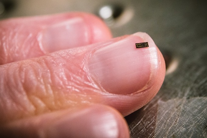
Comb generation techniques
Optical combs can be generated using many different techniques, and the suitability of each depends on the application.
They can be generated via mode-locking, in either solid-state (including fibre), or diode laser cavities. The solid-state type is the most widely deployed commercial comb source and offers excellent optical properties and a wide comb bandwidth. They are an excellent choice for laboratory and scientific work, but are less suited to low-cost, high-volume applications.
Mode-locked laser diodes on the other hand, do offer the potential for photonic integration. They have been explored deeply in the research community, for example through the EU FP7 project Big Pipes [1], and they are being actively commercialised for short reach communications.
A draw-back of mode-locked techniques in general is that they are based on a fixed physical cavity, and therefore the comb spacing is generally static. This limits swept-mode operation which can prove useful in applications such as spectroscopy and frequency metrology.
Optical combs can also be generated by over-driving electro-optic modulators. In order to get a high quality comb, numerous modulators (each requiring their own RF driver,) are typically used in series. This drives up the cost of the comb source, and also increases the optical loss, often necessitating the use of an optical amplifier which also limits commercial applicability.
Comb generators based on the Kerr effect in ring resonators are receiving much attention and many impressive results have been published recently on optical combs based on micro ring resonators. The efficiency of such devices can prove challenging, with external high-power pump lasers or amplifiers often required. However, more efficient devices, requiring less optical pump power are being actively developed, which provide excellent potential for low-cost commercial devices over time 2,3,4.
The reader is referred to the following references [5,6,7,8] for several far more detailed surveys and reviews of the various types and applications of optical combs. The remainder of this article focuses on gain switched comb generation from a monolithically integrated photonic chip a technique that offers a balance of simplicity, flexibility and performance.
Gain switched comb generation
The gain switching technique was originally used for short optical pulse generation. A semiconductor laser is directly modulated with a sine wave generating a series of short optical pulses with a repetition rate that is set by the frequency of the drive signal. Because the light in the laser cavity is completely extinguished during gain switching, the pulses are incoherent and therefore in the frequency domain, a broad continuous spectrum is observed. The use of an additional “master” laser to injection lock the gain switched “slave” laser can ensure that there is always light in the cavity, increasing the pulse to pulse coherence, and resulting in the set of discrete frequency tones that make up an optical comb.
The separation of the continuous wave (CW) master and modulated slave laser provides additional benefits. Through injection locking, the properties of the master laser including its linewidth are imparted on all of the comb lines. This offers the opportunity to optimise its parameters for optical quality, while optimising the slave for gain switching.
The ability to set the wavelength spacing using an RF frequency, as opposed to having it determined by a physical cavity, provides some of the key benefits of gain switched combs. With mode-locked diode lasers for example, the comb spacing accuracy is governed by the accuracy of the facet cleave and is often in the gigahertz range. In contrast, comb spacings accurate to sub-kHz levels can be achieved using gain switching. Furthermore, the distance between the comb lines can be swept with high accuracy and speed, enhancing applications such as spectroscopy and fibre sensing where swept wavelength tunable laser sources are regularly used to interrogate samples or sensors. This concept is illustrated in Figure 1.
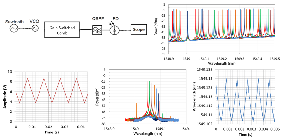
Figure 1: A sawtooth wave is used to sweep the voltage controlled oscillator that sets the comb spacing. One tone is locked in frequency by the master laser, while all other tones spread out from that point, as the comb frequency spacing is swept. In the example shown, a frequency discriminator consisting of an optical filter and a photodetector is used to capture the wavelength sweep.
Integrating the comb with active optical filtering for advanced applications
By integrating the master and slave lasers on a single chip, a photonic integrated comb source less than one square millimetre in footprint can be produced, while the electronics required to drive it are simple, and low-cost. Efforts are currently underway to produce optoelectronic comb source modules at prices and in form-factors typical of high-volume optical transceivers.
From this core building block of the comb PIC, even more powerful application specific PICs can be created through the integration of other components and structures. Active optical filters that allow one or more of the comb lines to be extracted and used for frequency shifting, frequency multiplication, frequency generation, or for modulating individual comb-lines with data are of particular importance. Three examples of the many applications enabled by this exciting technology are briefly described below.
Frequency metrology
By using integrated optical filters to select any two lines from a comb with tunable frequency spacing, an extremely versatile microwave, millimetre-wave, and sub-THz frequency generator can be created. An exciting application of this approach is in coherent population trapping (CPT), a technique used in rubidium atomic clocks. The photonic integrated comb architecture can be used to generate an optical signal consisting of just two coherent modes, spaced by the rubidium atomic resonance frequency, and centred on its absorption peak. By illuminating a vapour cell containing rubidium atoms and feeding back control signals from the detected light to the comb source, an atomically stable clock signal can be generated. Space agencies, academic researchers and commercial aerospace corporations are excited by the potential of this novel approach.
Optical networking
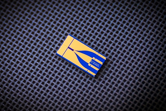
Almost all of the highest capacity, highest spectral efficiency optical transmissions ever carried out are based on optical combs, and yet, to date no comb-based coherent transceiver has made it to market. Today’s coherent transceivers employ one, or in some cases two optical carriers produced by independent lasers. Going beyond that to four or even eight wavelengths for terabit coherent transceivers poses cost, power and footprint challenges and comb sources have a role to play here. A key challenge has been the need to split the comb lines onto individual waveguides or fibres for data modulation, in a cost, size, and power efficient way. By monolithically integrating a gain switched comb source with a four or eight channel active optical filter, an on-chip demultiplexer can be created which separates the comb lines, amplifies them for external modulation and improves the carrier to noise ratio, while retaining the coherence between the lines. This disruptive technology makes optical combs a viable option for coherent transceivers for the first time, and is gaining the attention of several optical equipment vendors. (See Figures 2a and 2b)

Figure 2a (left) and Figure 2b(right) : (a) Pilot Photonics monolithically integrated comb source and demux PIC makes combs suitable for use in coherent optical transcievers for the first time. Ideally suited to 400G and 1T coherent transceivers, the chip delivers four coherent comb tones to separate fibers for modulation with data. (b) The chip and RF driver are co-packed in a high-speed optical package and light is coupled out using a four fiber array, allowing a single optical package to replace four individual laser packages that are used in typical transceivers. The Pilot Photonics device readily scales to greater channel counts.
Optical fibre sensing and spectroscopy
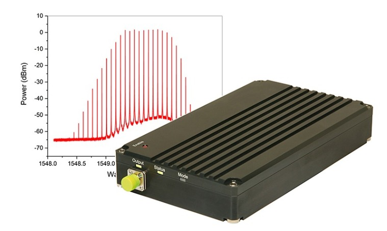
A third high-volume application of integrated optical combs is in dual comb spectroscopy, a powerful technique that uses two slightly offset combs to interrogate a sample, or a sensor. The benefits of dual-comb spectroscopy are that it provides a near real-time, high-resolution spectral output without any requirement for laser tuning. In effect, it transposes an optical measurement problem to the RF domain. Dual gain switched comb sources can easily be generated on a single chip, and an example is shown below. By coupling the power of the dual-comb technique with the cost and size benefits of photonic integration this architecture can unleash the potential of optical sensing by increasing the performance while reducing the cost and complexity of the laser systems required.
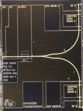
Figure 3: Pilot Photonics’ dual-comb Lyra-OCS-1000 is shown above
Pilot Photonics Lyra-OCS-1000 is the most cost-effective comb source on the market. Offering one-touch operation, it delivers a flexible gain switched comb from a fully integrated opto-electronic module.
Conclusion
Optical combs have been duly recognised as one of the most important technologies of our time as they form a bridge between the RF and optical worlds. Their intersection with photonic integration creates wonderful possibilities and offers the potential for truly disruptive innovation, which will see their widespread deployment in numerous high-volume applications. Gain switched comb generation is a powerful and versatile approach that offers the potential for ultra-low cost implementation. (Figure 3) If you have an application to which it could be applied, please get in touch with Pilot Photonics.
1 www.bigpipes.rwth-aachen.de/
2 Jiang Li, Hansuek Lee, Tong Chen, Kerry J. Vahala “Low-Pump-Power, Low-Phase-Noise, and Microwave to Millimeter-wave Repetition Rate Operation in Microcombs”, Phys. Rev. Lett. 109, 233901 (2012)
3 Daryl T. Spencer, et al “An optical-frequency synthesizer using integrated photonics”, Nature volume 557, pages81–85 (2018)
4 P. Trocha, et al, “Ultrafast optical ranging using microresonator soliton frequency combs”, Science, 23 Feb 2018 : 887-891
5 M. Imran, P. M. Anandarajah, A. Kaszubowska-Anandarajah, N. Sambo and L. Potí, "A Survey of Optical Carrier Generation Techniques for Terabit Capacity Elastic Optical Networks," in IEEE Communications Surveys & Tutorials, vol. 20, no. 1, pp. 211-263, First quarter 2018.doi: 10.1109/COMST.2017.2775039
6 V. Torres-Company and A. M. Weiner, “Optical frequency comb technology for ultra-broadband radio-frequency photonics,” Laser Photon. Rev. , vol. 8, no. 3, pp. 368–393, 2014, doi:10.1002/lpor.201300126
7 P. J. Delfyett et al. , “Advanced ultrafast technologies based on optical frequency combs,” IEEE J. Sel. Topics Quantum Electron. , vol. 18, no. 1, pp. 258–274, Jan./Feb. 2012.
8 S. A. Diddams, “The evolving optical frequency comb [invited],” J. Opt. Soc. Amer. B , vol. 27, no. 11, pp. B51–B62, Nov. 2010. [Online]. Available: http://josab.osa.org/abstract.cfm?URI=josab-27-11-B51
SSE Enterprise Telecoms has revealed details of its biggest network technology investment in the UK to date with the introduction of a new technology platform based on optical networking firm Infinera's XTM Series of packet optical solutions.
The UK government outlined in its 2017 digital strategy vision the need to ‘continue to create conditions that encourage investment in the UK’s digital infrastructure’. The SSE/Infinera announcement is designed to improve connectivity for all UK businesses by creating a credible UK alternative to costly new cable laying projects. SSE will offer a resilient, ‘dark fibre-like’ network on a large scale.
SSE chose to partner with Infinera due to its unique combination of layer 1 and 2 packet optical and Ethernet services – serving as a credible alternative to customers laying costly dark fibre cabling. Infinera’s impressive synchronisation capabilities allow for flexibility on the network, not currently available at such scale or at an accessible price point for SSE Enterprise Telecoms’ customers.
The extensive network promises access to multiple services with speeds of up to 100 gigabits per second to each BT exchange. Current networks are only able to offer a fraction of those speeds at a commercially viable cost.
Customers of the SSE Enterprise Telecoms’ network will benefit from connectivity to more than 80 commercial data centres, meaning it’ll be able to meet them practically anywhere. UK businesses and service providers will have the flexibility and option to scale, supported by a high-capacity network without any upfront cost required to buy or lay new fibre connectivity to each exchange.
Conrad Mallon, chief technical architect, SSE Enterprise Telecoms says: “We’re working with Infinera because they have an elegant product set that scales effectively, and a unique approach to layer 1 and 2 connectivity. A network project on this scale makes us one of the few providers that can offer multiples of 100Gbps services between exchanges, commercial data centres and across our core, at an accessible price point. The network expansion deal is also paving the way for our ambitious roadmap which will see SSE Enterprise Telecoms investing more in network reach over the next five years.”
Nick Walden, SVP, EMEA, Infinera says: “The UK market has never been more dynamic, now facing exponential bandwidth growth coupled with a renewed focus on connectivity services from both enterprises and carriers due to the recent DFA activities. Infinera is delighted to partner with SSE Enterprise Telecoms on this significant project to rapidly scale network capacity and service differentiation for its customers with our leading XTM Series packet optical solutions.”
Finisar has announced an upcoming ribbon-cutting ceremony to celebrate its new manufacturing facility in Sherman, Texas. Finisar will use the site to increase production capacity of its VCSELs and related 3D Sensing technologies, used in a wide range of applications. The ribbon-cutting event will be held on Monday, July 9th with speakers from Finisar’s executive management team, including CEO Michael Hurlston, as well as local community leaders.
Finisar has been working diligently to prepare the site for operations. The building, formerly owned by MEMC and SunEdison, has been under renovation since December 2017 and is on target to commence production by the end of this calendar year. It is currently certified as clean room operational and the first production tooling has been installed and qualified. The company has hired nearly 200 employees, including the operations and support staff necessary to begin production. Finisar expects to expand hiring further later this year to support the anticipated ramp to high volume production.
“Finisar is excited to unveil this new state-of-the-art facility which will expand critical production capacity of our VCSEL products needed to support customer requirements,” said Michael Hurlston, Finisar’s CEO. “We are also pleased to create hundreds of manufacturing jobs in the US and to hire talent from the local area as we work together to make Sherman the VCSEL Capital of the World.”
Originally used by Finisar in its optical communication products, VCSEL technology is extending the possibilities of consumer and scientific applications including 3D facial recognition, augmented reality, automotive in-cabin sensing and automotive LIDAR.
The wide-spread adoption of optical transceivers in a broad range of applications is urgently calling for a low-cost, high power efficient and large volume manufacturing integration technology that can meet the different specifications required in every application sector.
Current solutions favour silicon photonics based technologies that still feature a major drawback: namely they need complex and expensive hybrid integration substrates, since they rely on externally coupled InP laser sources for the final assembly. Meanwhile, the testing for the pre- and post- processed coupled laser adds further costs.
MOICANA is a new ambitious EU H2020 R&D Project which was launched early in 2018. It aims to develop fundamental innovations in the field of photonic integrated transmitters, making them cheaper and more power efficient.
The consortium is bringing together four industrial partners, and four academic and research institutes in the PIC and Photonic Systems value chain. The project participants are the Aristotle University of Thessaloniki (Greece), University of Kassel (Germany), Technion- Technical University of Israel (Israel), III-V lab (France), Mellanox Technologies (Israel), Ligentec (Switzerland), ADVA (Germany) and VLC Photonics (Spain).
MOICANA is funded under the H2020 ICT 2016-2017 – Photonics KET Call and the initiative of the Photonics Public Private Partnership. The project is coordinated by Aristotle University of Thessaloniki in Greece and will be running through to December 2020.
MOICANA aims to demonstrate breakthrough performance by combining Quantum Dot InP structures as the III-V light source material and SiN from the silicon photonics for the passive platform. The ideas is to minimise the cost of high volume fabrication of optical transmitters through the development of technology for epitaxy of the QD InP components directly on Si by selective area growth.
The project partners aim to the demonstrations of a whole new series of cooler-less, energy-efficient and high-performance single-channel and WDM transmitter modules for data centre interconnects, for 5G Mobile fronthaul and for coherent communications.
Microsystem and nanotechnology systems developer CMC Microsystems and Advanced Micro Foundry (AMF), a Singapore-based manufacturer of silicon photonic integrated circuits, are partnering to develop a new design automation platform for silicon photonics that will allow Canadian university researchers to take the lead in developing innovations in light-based technologies.
“A key value-add of this platform is its physical design kit (PDK), which is one of the most advanced created for photonics R&D,” said Dan Deptuck, staff scientist at CMC Microsystems. “It enables unprecedented first-time-right design of more complex systems more quickly, and its industrial approach speeds up time to market.”
The new CMC-AMF Silicon Photonics Platform allows innovators to design and prototype photonics-based technologies faster and more successfully. It includes a design kit, developed by AMF with partner Luceda Photonics, access to AMF’s fabrication services, and design tools from Luceda and Mentor Graphics Corp.
“Canada continues to make its mark as an innovator in this rapidly expanding technology field, and CMC has been a pioneer in enabling university-based silicon photonics R&D,” says Gord Harling, president and CEO of CMC Microsystems. “To date, we have helped innovators in Canada’s National Design Network prototype more than 500 projects in silicon photonics, and we have trained more than 400 students. Now, thanks to our partnership with AMF, we are able to increase our offerings to researchers, making it easier for them to access technologies and opportunities for advancing their photonics research and development. This translates directly into a technological advantage for a Canadian industry sector that is experiencing strong growth.”
CMC will provide platform users with engineering support, reference guides, and training, and will coordinate manufacturing of designs via its cost-effective multiproject wafer program. CMC is providing the platform to academic researchers and industry across Canada’s National Design Network and also internationally.
“CMC Microsystems has been a valued partner with us since 2012,” said Kavitha Devi Buddharaju, senior manager of business development at AMF. “As a proven service provider and global facilitator of multiproject wafer services in silicon photonics, they are perfectly positioned to help us bring our technology to clients around the world. This partnership will enhance our mutual efforts to help researchers and companies realize the potential of silicon photonics.”
AMF specializes in customizable prototyping and volume wafer manufacturing services for silicon photonic integrated circuits. CMC works with researchers and industry to provide industrial capabilities for the design and manufacture of innovations in microsystems and nanotechnologies.
POET Technologies, a designer, developer and manufacturer of optoelectronic devices, including light sources, passive wave guides and Photonic Integrated Circuits (PIC), has executed an agreement for the co-development of transmit device solutions with Almae Technologies, a France-based manufacturer of photonic products. The purpose of the agreement is to jointly develop, manufacture and sell a series of laser modules based on the POET Optical Interposer platform into high-speed data communication applications.
The companies will collaborate on designs of lasers and modulators to be compatible with POET’s Optical Interposer and to provide foundry services for both epitaxial supply and device fabrication. The collective efforts of the two companies will be carried out through a series of overlapping projects, covering the exchange of data and techniques, co-development activities, commercial arrangements, and strategies for pursuing global go-to-market sales.
POET’s CEO, Suresh Venkatesan, commented: “We are very pleased to establish a framework for collaboration with Almae, a leading European supplier of high-performance EML lasers based on a novel buried heterostructure design and an advanced PIC fabrication platform. In addition to the joint development of Optical Interposer-compatible devices, the agreement outlines an arrangement for sharing expertise and resources to accelerate time-to-market for both companies, while also expanding our collective geographic reach and providing a much larger market opportunity.”
Jean-Louis Gentner, COO of Almae Technologies, stated: “The framework for collaboration with POET follows closely behind the recent introduction of our 25G integrated laser-modulator (25G EML), which has broad application in high-performance photonics. The inclusion of our device designs into the POET Optical Interposer platform will expand the applications we can address in both the datacom and telecom markets. We are also pleased to be able to offer our epitaxial foundry services to POET and to take advantage of POET’s fabrication capabilities in Singapore.”
Optical communications firms Acacia and Oclaro are working together to create fully interoperable CFP2-DCO (digital coherent optics) modules based on Acacia's Meru DSP.
Oclaro plans to launch a new CFP2-DCO module that will feature plug-and-play compatibility with the Acacia CFP2-DCO, providing customers with two proven coherent optics suppliers for the 100/200G CFP2-DCO form factor.vThe modules will support transmission speeds of 100G and 200G for use in access, metro and data centre interconnect markets.
CFP2-DCOs are becoming increasingly important for higher-speed optical networks because they integrate the coherent DSP into the pluggable module. The digital host interface enables simpler integration between module and system resulting in faster service activation and a pay-as-you-grow deployment model for telecommunication providers whereby the cost of additional ports can be deferred until additional services are needed.
"Our 43Gbaud Coherent Transmitter Receiver Optical Sub-Assembly (TROSA) is at the heart of our CFP2-DCO. The TROSA leverages InP PIC technology from Oclaro's highly successful CFP2-ACO to achieve industry leading optical performance in a small form factor," said Beck Mason, president of the Integrated Photonics Business at Oclaro. "By establishing a fully interoperable solution with Acacia, our customers will have two sources of supply for these critical components, enabling them to efficiently upgrade their networks to higher speeds."
The CFP2-DCO form factor is being introduced by multiple network equipment manufacturers (NEMs) in switch, router, and transport platforms. The CFP2-DCO modules support four times higher density than current generation 100G CFP-DCO solutions by doubling the data rate in a smaller, lower power, pluggable module enabling customers to quickly and cost-effectively roll-out 200G networks. In addition to proprietary operating modes, both companies intend to support the requirements of the Open ROADM MSA for interoperability at 100G.
"Network operators and our system partners are excited about the ramp of our CFP2-DCO module," said Benny Mikkelsen, CTO of Acacia Communications. "By partnering with Oclaro to ensure interoperability with their Meru-based CFP2-DCO module, we believe we will be better positioned to address the DCO market as industry trends shift favorably toward the CFP2 form factor. We are excited about our relationship with Oclaro and believe that broader adoption of 200G CFP2-DCO modules will be mutually beneficial to our two companies and the customers we serve."
Researchers at AMO GmbH, a non-profit SME based in Aachen, have used Oxford Instruments Plasma Technology’s fabrication solutions to develop a graphene based photonics detector device capable of operating at a data rate of 25 Gb/s per channel. The device converts optical modulation data into an electrical signal.
Oxford Instruments offers solutions for the data communications market for both scaled-up production as well as novel device R&D. The detector fabrication solution includes: waveguide fabrication, III-V/2D materials mesa etching and graphene/2D/novel materials deposition. In addition Oxford Instruments also offers a range of solutions for devices such as the InP edge emitting lasers and VCSELs for photonic data communications.
Devices developed by scientists at AMO within the European Graphene Flagship project have set the yardstick in terms of high speed photodetectors operating at telecom wavelengths. At the Mobile World Congress in Barcelona this year, AMO scientists along with collaborators with the Graphene Flagship project demonstrated the world’s first graphene data communication link operating at 25 Gbits/s per channel. As such the detector developed at AMO can reach speeds of up to 130 GHz.
“We are extremely delighted to see the progress made by researchers at AMO on our device fabrication solutions”, says Frazer Anderson, innovation and solutions director, Oxford Instruments Plasma Technology. He continued:” We continue to invest in further developing and improving our cutting edge device fabrication processes for datacomms and photonics through feedback from such impressive success stories.”
Max Lemme, managing director, AMO GmbH comments: “The latest results on high-speed graphene-based data communication are very encouraging. They are a positive testament to AMO’s mission: to identify new materials and to demonstrate new technologies for future applications in electronics and optoelectronics, such as IOT and 5G. We can only achieve such results through our state-of-the-art R&D process line, which includes a large number of tools for scalable nanotechnologies, such as Oxford Instruments’ RIE, ALD and CVD tools”
The devices were developed at AMO’s 6inch device fabrication pilot line equipped with Oxford Instruments fabrication solutions which includes ICP RIE, ALD and PECVD tools.
Technique would allow addition of optical communication components to existing chips with little modification of their designs.
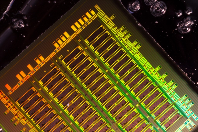
Researchers have developed a technique for assembling on-chip optics and electronic separately, which enables the use of more modern transistor technologies. Image: Amir Atabaki
Two and a half years ago, a team of researchers led by groups at MIT, the University of California at Berkeley, and Boston University announced a milestone: the fabrication of a working microprocessor, built using only existing manufacturing processes, that integrated electronic and optical components on the same chip.
The researchers’ approach, however, required that the chip’s electrical components be built from the same layer of silicon as its optical components. That meant relying on an older chip technology in which the silicon layers for the electronics were thick enough for optics.
In the latest issue of Nature, a team of 18 researchers, led by the same MIT, Berkeley, and BU groups, reports another breakthrough: a technique for assembling on-chip optics and electronic separately, which enables the use of more modern transistor technologies. Again, the technique requires only existing manufacturing processes.
“The most promising thing about this work is that you can optimize your photonics independently from your electronics,” says Amir Atabaki, a research scientist at MIT’s Research Laboratory of Electronics and one of three first authors on the new paper. “We have different silicon electronic technologies, and if we can just add photonics to them, it’d be a great capability for future communications and computing chips. For example, now we could imagine a microprocessor manufacturer or a GPU manufacturer like Intel or Nvidia saying, ‘This is very nice. We can now have photonic input and output for our microprocessor or GPU.’ And they don’t have to change much in their process to get the performance boost of on-chip optics.”
Light appeal
Moving from electrical communication to optical communication is attractive to chip manufacturers because it could significantly increase chips’ speed and reduce power consumption, an advantage that will grow in importance as chips’ transistor count continues to rise: The Semiconductor Industry Association has estimated that at current rates of increase, computers’ energy requirements will exceed the world’s total power output by 2040.
The integration of optical — or “photonic” — and electronic components on the same chip reduces power consumption still further. Optical communications devices are on the market today, but they consume too much power and generate too much heat to be integrated into an electronic chip such as a microprocessor. A commercial modulator — the device that encodes digital information onto a light signal — consumes between 10 and 100 times as much power as the modulators built into the researchers’ new chip.
It also takes up 10 to 20 times as much chip space. That’s because the integration of electronics and photonics on the same chip enables Atabaki and his colleagues to use a more space-efficient modulator design, based on a photonic device called a ring resonator.
“We have access to photonic architectures that you can’t normally use without integrated electronics,” Atabaki explains. “For example, today there is no commercial optical transceiver that uses optical resonators, because you need considerable electronics capability to control and stabilize that resonator.”
Atabaki’s co-first-authors on the Nature paper are Sajjad Moazeni, a PhD student at Berkeley, and Fabio Pavanello, who was a postdoc at the University of Colorado at Boulder, when the work was done. The senior authors are Rajeev Ram, a professor of electrical engineering and computer science at MIT; Vladimir Stojanovic, an associate professor of electrical engineering and computer sciences at Berkeley; and Milos Popovic, an assistant professor of electrical and computer engineering at Boston University. They’re joined by 12 other researchers at MIT, Berkeley, Boston University, the University of Colorado, the State University of New York (SUNY) Polytechnic Institute, and Ayar Labs, an integrated-photonics startup that Ram, Stojanovic, and Popovic helped found.
Sizing crystals
In addition to millions of transistors for executing computations, the researchers’ new chip includes all the components necessary for optical communication: modulators; waveguides, which steer light across the chip; resonators, which separate out different wavelengths of light, each of which can carry different data; and photodetectors, which translate incoming light signals back into electrical signals.
Silicon — which is the basis of most modern computer chips — must be fabricated on top of a layer of glass to yield useful optical components. The difference between the refractive indices of the silicon and the glass — the degrees to which the materials bend light — is what confines light to the silicon optical components.
The earlier work on integrated photonics, which was also led by Ram, Stojanovic, and Popovic, involved a process called wafer bonding, in which a single, large crystal of silicon is fused to a layer of glass deposited atop a separate chip. The new work, in enabling the direct deposition of silicon — with varying thickness — on top of glass, must make do with so-called polysilicon, which consists of many small crystals of silicon.
Single-crystal silicon is useful for both optics and electronics, but in polysilicon, there’s a tradeoff between optical and electrical efficiency. Large-crystal polysilicon is efficient at conducting electricity, but the large crystals tend to scatter light, lowering the optical efficiency. Small-crystal polysilicon scatters light less, but it’s not as good a conductor.
Using the manufacturing facilities at SUNY Polytechnic Institute's Colleges of Nanoscale Sciences and Engineering, the researchers tried out a series of recipes for polysilicon deposition, varying the type of raw silicon used, processing temperatures and times, until they found one that offered a good tradeoff between electronic and optical properties.
“I think we must have gone through more than 50 silicon wafers before finding a material that was just right,” Atabaki says.

The 400G CWDM8 Multi-Source Agreement (MSA) Group has identified and approved new open optical interface specifications for 400G interoperability in data center applications. By: Scott Schube, Project Chair, CWDM8 MSA Group
The drive for 400G
CWDM8 requirements for data center applications
Compatibility with networking equipment and next-generation module form factors
Full multi-vendor interoperability over an optical link
Support for low-power implementations
Proven technology with ability to scale
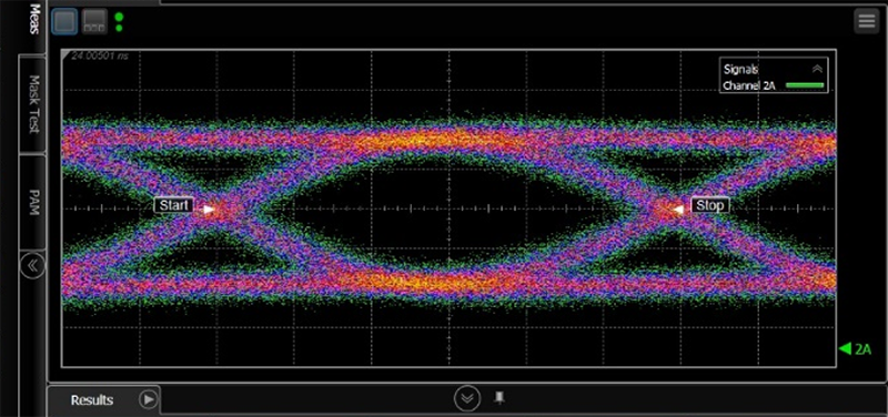
50Gbd NRZ optical eye diagram
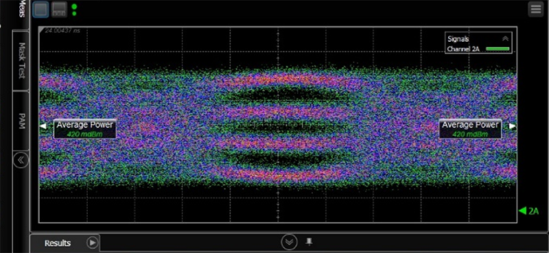
50Gbd PAM4 optical eye diagram
Path to future interfaces beyond 400G
CWDM8 status and next steps
After technical discussions, the CWDM8 MSA Group has released both the 2 km and 10 km 400G MSA optical interface specifications, both of which are available at www.cwdm8-msa.org. 400G optics products based on the CWDM8 MSA will be available soon and will help enable the 400G interconnect transition in data centers in 2018-19 and beyond.
With numerous reports placing PIC market growth at a CAGR [1] upwards of 20% until 2022 and beyond, advanced automation for assembly and testing are crucially needed to enable high volume production at viable costs per part. By: Ignazio Piacentini, Gregory Flinn
Photonics technology is undergoing a transition toward greater integration, with multiple functionality and components being combined onto a single chip or within a small hybrid assembly – also known as a photonic integrated circuit, or PIC. In catering to the burgeoning telecom and datacom demands (internet communications and data centers for cloud services, respectively), development has been directed at meeting requirements in terms of bandwidth density and power dissipation. That is, absolute processing power is no longer the main concern, but moving data in and out – efficiently – is of paramount concern. Having found a solution in photonic integrated circuits, these sectors have been the driving force behind their advancement.
With photonics being widely recognized as an essential enabling technology for a broad spectrum of industrial processes and applications, the PIC idea has naturally ‘trickled over’, simultaneously providing greater breadth to the growing infrastructure needed to support PIC eco-systems. Many now consider the technology infrastructure as mature enough to become mainstream.
The emerging PIC applications
Aside from telecom and datacom PIC applications, there a number of other strong market opportunities exploiting similar IR wavelengths (thus benefiting from the existing development maturity at those wavelengths), as well as a broad selection of applications that have traditionally sought to utilize miniaturization at more visible wavelengths.

Figure 1: LIDAR and other optical sensor applications for automotive are set to grow significantly (iStock.com/pixelfit)
Some of the former include the increasingly sophisticated optical sensing devices designed for (progressively autonomous) automotive applications. A growing number of optical sensing devices, including LiDAR [2], are being integrated into diverse automotive transport platforms, entering into a sector that is expected to experience a significant upheaval [3] over the next 15 to 20 years.
Other markets to consider include augmented and virtual reality applications, in particular where they impact consumer markets; biophotonics, OCT and other biomedical sensing devices for decentralized testing (point-of-care diagnostics enabled by optofluidic and/or BioMEM devices); making more ‘sense’ of the environment around us via a multitude of networked sensors, typically referred to as Internet of Things (IoT) applications; as well as RF photonics for aerospace and defense, quantum systems, terahertz technology, and others.
If the market forecasts are to be believed, the integrated opto-electronic devices feeding into these applications will need to be manufactured, assembled, tested and ultimately suitably packaged at high volume.

Figure 2: Augmented/virtual reality applications exhibit the volume scales that justify PIC use
Gearing up for high volume
For most of the application spaces for photonics, device production has traditionally been geared to volumes between hundreds and thousands of components. Photonics and micro-electronics components have been individually manufactured and integrated discreetly, then assembled as a complete device, tested and finally packaged. However, for larger numbers of photonic devices, perhaps hundreds of thousands or millions, ‘individual’ and ‘discrete’ are no longer viable procedures.
It is true that for PIC approaches the diverse active/passive functional elements still need be combined (in this case, hybridized) onto a base platform. That is, there is no single technology platform that delivers all of the functionality required, instead there are several different material systems contributing diverse functional building blocks to the PIC eco-system. The trick then is to ensure that these are highly integration-capable, thus lending themselves to a wafer-level approach to assembly & test, and pushing singulation as far down the production line as possible. This, incidentally, is much as has been the case for CMOS – in reducing element diversity by rationalizing them down to a reduced number of mutually compatible micro-platforms, a pathway to high volume and wafer-scale production is opened up.
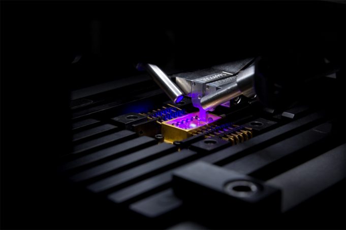
Figure 3: Discrete assembly and test approaches have been acceptable at low volumes, but are entirely unrealistic at much higher manufacturing volumes.
Notably, the move towards greater opto-electronic integration actually necessitates a convergence of photonics and electronics not only in terms of component manufacturing, but across all aspects of production, meaning design, manufacturing, assembly, test and packaging. The principal caveat to this idea is that the current (elementary) development status of the PIC eco-system infrastructure stands in distinct contrast to the robust maturity, scale (i.e. numbers of wafers) and automation level common to CMOS processes for micro-electronics production.
With the disparity between infrastructure maturity for PICs as compared to CMOS amounting to something like four decades, this convergence will not happen overnight. Still, there may be real opportunities to carry the know-how gained in CMOS directly over. For example, the in-line test procedures implemented within CMOS have been instrumental in reducing the cost of assembly, testing and packaging of conventional CMOS chips down to the order of 10-20% of the total production cost. For photonics in general, these are by far the largest cost factor.
Optical assembly and testing procedures as the bottleneck
The overall production task for PICs is conceptually the same as for conventional micro-electronics. It is the optical probing aspect that introduces greater complexity:
The consequences of these unique requirements are twofold and stand at odds with the notion that CMOS know-how can be directly transported over to PICs. Firstly, assembly processes for PICs last from a few tens of seconds to several tens of minutes, placing strict requirements on the complexity of machinery designed to achieve these tasks. Even for the discrete assembly of singulated PICs into devices, it is very difficult to achieve sufficiently short cycle time without jeopardizing yield.
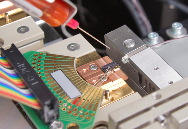
Figure 4: Coupling a fiber array to a PIC using an alignment system with 6 degrees of freedom
Secondly, testing procedures gain another layer of complexity, as PIC testing requires both optical and electrical probing. Each requires very different positional accuracy, and each carries its own set of parameter-specific requirements (DC /low frequency and RF for electrical).
In solving these issues, a typical hybrid optical/electrical probe head for PICs will most likely need to exhibit a layout that caters first to the more demanding optical requirements. Indeed, ficonTEC has already been pursuing exactly this approach in certain projects and initiatives, and an opportunity to explore requirements in a real manufacturing setting would be invaluable.
The generally accepted (albeit somewhat out-of-date) situation for PICs [4] is that front-end procedures contribute only 20% to the overall cost of production, while back-end procedures (assembly, testing and packaging) contribute around 80%. To be fair, we now have to consider a combined suite of electrical and optical testing procedures, so it would be unrealistic to expect parity with CMOS in this respect. Still, it may be reasonable to assume that the adoption of established CMOS-style in-line test infrastructures and procedures (at least as far as is practicable) can go some way to alleviating back-end costs.
Assembly & test for higher volumes
Increasing volumes will necessitate a transition to wafer-level-capable procedures. In the wafer environment, coupling type/speed/accuracy, overall pin count, and diverse optical test parameters all present varying issues along the process chain. Additionally, for the many optical features present on a PIC that generate heat or that are temperature-sensitive, thermal considerations become more dominant.
The specialized requirements of PIC device manufacture have elevated testing as an increasingly integral part of the assembly cycle since reworking following any assembly step is almost impossible in most applications. Nonetheless, such issues can be eased through utilizing careful design in the development phase by explicitly detailing what needs to be tested, when and to what level of requirements, and by providing the appropriate probing approach.
In terms of coupling, edge coupling offers certain practical advantages [5] but is usually not accessible before dicing unless additional intermediate process steps are introduced. Vertical grating couplers (VGCs) provide device access at wafer level, with one approach incorporating VGCs as temporary ‘test only’ structures during manufacture (removable optical test-points’) [6]. A combination of both – surface coupling for wafer-level testing even when edge-coupling the packaged device – is also an option.
Characterization procedures also need to be considered. These can occur both at the module level, and in terms of a post-process device qualification test, and with in-line characterization and final device testing posing perhaps very different requirements. In addition, these procedures need to account for the application-specific needs, i.e. environmental and/or hermiticity needs differ widely between Telcordia and biomedical applications. Finally, there may be third party tests that need to be incorporated.
In general, it will be the optical followed by electrical I/O requirements that will define the assembly layout and associated process requirements in PIC production. Ideally, electrical, optical, layout and fixturing issues should be considered as early as possible so as to minimize conflicts. Unfortunately, these considerations still draw largely from the immediate device-specific needs, rather than addressing aspects such as automated assembly and scalability. High-volume products in particular tend to lean toward specifically adapted solutions to achieve optimum size, best performance, and/or cost savings.
Experience suggests that an ‘optical first’ approach may prove more favorable. What is needed are practical concepts for pre-alignment of optical probing, some degree of parallelism for wafer-level testing, and this in combination with optical/electrical probe approaches. At the same time, there is no way around the implementation of greater automation.
Projects & initiatives
In just one of many parallel activities geared toward a higher level of photonics integration, ficonTEC has been awarded an order by AIM Photonics [7] for a new wafer-level tester complete with robotized wafer loading. The system is designed to flexibly handle all electrical and optical testing procedures for singulated chips and wafer level, with fully automated test cycles for both vertical grating and edge couplers.
Another collaboration with PIXAPP [8], is providing a route to small and medium-volume production of packaged PICs. Coordinated by the Tyndall National Institute [9] in Cork, Ireland, solutions will be developed for four different application domains – bio-sensing, fiber sensing, telecom and datacom – each with its own suite of specific challenges in terms of packaging, costs and expected reliability. PIXAPP will provide industrial users with single-point access to a complete overview of the PIC supply chain, linking design tools to automated assembly, test and packaging. In the long-term interaction with diverse partners and their requirements, ficonTEC hopes to develop a better understanding of PIC assembly and testing needs in different market segments.
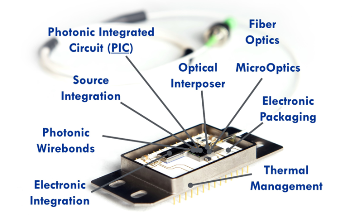
Figure 5: Key focus areas for the PIXAPP photonics packaging pilot line (courtesy of PIXAPP)
In addition to these readily visible activities, ficonTEC has gained significant experience working together with a number of high-profile global technology leaders on projects that already require wafer-level processes in production. Highlights from just a few of the many projects mirror some of the themes discussed above:
ficonTEC always works very closely with the customer development teams to fully understand the requirements, and then tune these within the framework of the available system capabilities, or, alternatively, work with the customer to develop those needed. In some cases, these collaborations are already implementing necessary process and system changes for upscaling the production – not simply as multiple production lines operating in parallel on the same suite of tasks, but also with an additional layer of control provided by a common revision control server. Individual process as well as system-wide updates can now be implemented automatically and remotely.
In moving to ever higher production numbers, and simultaneously trying to balance production cost against device sophistication, there will certainly be no way around the adoption of these advanced automation procedures.
Outlook
While the hurdles to speeding assembly and test for PICs seem to be many, this is not to say that photonic device production cannot be improved through process development and increased automation. Additionally, as was the case for micro-electronics, standards defining the overall eco-system will emerge, ultimately leading to more efficient assembly & test systems.
ficonTEC’s own activities in assembly, testing and packaging for photonic devices continues to grow. This expertise – comprising over 600 installed systems globally since 2001, with 85 alone in 2017 and 50 in Q1 2018 – has shown that these still almost exclusively come with very diverse requirements. Irrespective of this, the common aspect in developing all of these systems has been the timely design of the production process around the tools available.
References
[1] Examples of market researchers predicting substantial PIC
market growth potential:
[2] LiDAR Technology:
[3] Automotive sector volatility and growth potential:
[4] PIC roadmap example: JEPPIX Roadmap 2018, p.37
[5] ‘Wafer-scale high-density edge coupling for high throughput testing of silicon photonics’, R. Polster, et al, OFC 2018 – see also AIM Photonics
[6] ‘Towards autonomous testing of photonic integrated circuits’, M. Milosevic, Proc. SPIE 10108, Silicon Photonics XII, 1010817 (2017/02/20)
[7] Link to Aim Photonics: http://www.aimphotonics.com/
[8] Link to PIXAPP: https://pixapp.eu/
[9] Link to Tyndall National Institute: https://www.tyndall.ie/about-us
[10] Link to Euratom EU Horizon 2020 program information: https://ec.europa.eu/programmes/horizon2020/en/h2020-section/euratom
[11] Link to EMVA program information: http://www.emva.org/
Authors
Ignazio Piacentini has a B.Sc. in Nuclear Engineering and a M.Sc. degree in Digital Systems and Instrumentation. Following early participation in the EC’s Euratom [10] he joined the machine vision industry in the early 1990s, later held the position of Business Development Manager Europe for Imaging & Motion of National Instruments, subsequently founded ImagingLab Srl, and has also served two, three-year mandates as a member of the Board of Directors of EMVA [11] (European Machine Vision Association). Ignazio Piacentini took up the position of Business Development at ficonTEC in 2015, after previously heading up the Photonics Devices Assembly BU at PI miCos GmbH (Physik Instrumente Group).
Dr. Gregory Flinn has over 30 years of experience with learning, teaching, R&D, journalism, report generation, international marketing as well as business development in laser technology and photonics-related applications. Located close to Munich, Germany, he provides independent photonics market support under the guise of Putting Photonics into Context. He can be reached at mail@gregoryflinn.net.
Contact
ficonTEC Service GmbH,
28832 Achim, Germany
Tel.: +49 4202 511 60-0
Fax: +49 4202 511 60-090
E-Mail: info@ficontec.com

The solution for next-generation data processing requirements can be found by incorporating silicon photonic technologies in high performance computing (HPC) applications, according to researchers at CEA-Tech who have developed and prototyped new optical network on chip (ONoC) designs. By: Yvain Thonnart, CEATech – LETI, Design, Architecture & Embedded Software Division; Stéphane Bernabé and Vincent Reboud, CEATech – LETI, Photonics Division
In the past years, silicon photonics technology has matured to the point that it can be used in commercial products. For instance, photonic transceivers now connect racks optically in data centers, with data rates from 100 Gbps and beyond. Such products are delivered by several companies, such as Intel, Mellanox, Luxtera, and so on, and will shortly reach 400 Gbps using WDM (Wavelength Division Multiplexing) techniques and advanced modulation formats (e.g. PAM-4) in transceiver modules. As a result, silicon photonics will increasingly compete with other technologies like VCSELs and InP based modules, with an intrinsic advantage in term of scalability, and mass manufacturing capability. There is little doubt that silicon photonics will also soon address new markets and applications including optical sensors and high performance computers (HPC).
Regarding HPC, optical solutions have been considered for a long time as an obvious way to improve the performance of computing systems in term of energy efficiency, bandwidth density and latency. Optical links can indeed be used to interconnect memories to processors or several processors within a supercomputer (such as IBM Power 775). In addition, on-chip optical buses have also been proposed to optically connect cores together in ‘manycore’ computing systems. These latter architectures are known as “optical network on chipo” (ONoC). They rely on several concepts which have been made available by merging silicon photonics building blocks (particularly microring modulators) and advanced packaging technologies (particularly micropillar-based flip-chip assembly).
The typical diameter of microring based modulators and the typical pitch of micropillar interconnects are in the range of few to several tens of micrometers. Those critical dimensions allow the dense connection of several computing multicore processor chips (called chiplet) reducing dramatically their footprint and can be 3D stacked on top of a photonic interposer, embedding the various optical functionalities of light modulation, detection and guiding. As a result, a communication network between chiplets is created, using WDM: every chiplet needs to communicate with the others and to primary inputs and outputs (I/O) of the assembly on the interposer.
To this end, LETI proposed an optical network topology using one waveguide per transmitter, whether chiplet or primary I/O, which will pass through all receivers. The required data bandwidth is transmitted on the corresponding number of wavelengths depending on the target data rate, using microring modulators. The receivers use microring filters to route the light to their own photodetectors depending on the destination of the data flow, forming a circuit-switched optical network. In order to allow tiling of identical chiplets on top of this optical interposer, the waveguides form a ring of concentric spirals, which also avoids crossings between waveguides, as shown on Figure 1.
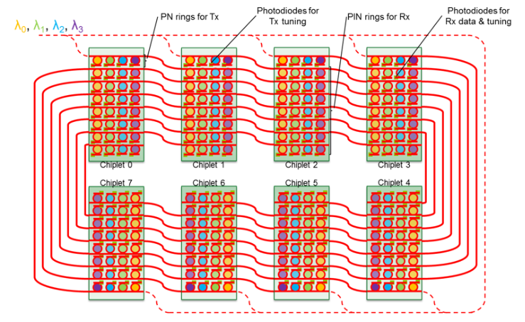
Figure 1: Leti’s proposal for an optical network topology utilizes one waveguide per transmitter, whether chiplet or primary I/O, which will pass through all receivers.
The silicon photonic circuit embeds the various aforementioned building blocks available within Leti’s R&D fabrication platform. This platform includes a standard manufacturing process and a device library that can be used to design complex circuits within an automated design environment including layout, device compact models and verification tools. This toolbox forms a unique photonic design kit (PDK), which has been developed within the IRT Nanoelec Photonic Program, a French consortium involving CEA LETI, Mentor Graphics and ST Microelectronics, among others. It is available in several CAD environments, e.g. Mentor Pyxis.

Figure 2: Several typical building blocks are needed in an Optical Network On Chip (ONoC). From left, these include: a ring modulator, a photodiode and an optical bus.
All device structures needed for on-chip optical networking are processed utilizing Silicon On Insulator (SOI) base wafers, within a standard process flow that includes silicon patterning, silicon doping (for light modulation and carrier collection) and local germanium epitaxy to build high speed photodiodes at the end of waveguides. Other available building blocks are ring filters, Mach-Zehnder modulators, multiplexers and power splitters. The process ends with a two-layer back end of line (BEOL) step for electrical wiring and a specific post process to grow the copper micropillars, with a typical pitch of 40 µm.
To give more flexibility to designers, LETI is also developing technological add-ons to the standard process flow, such as III-V material hybridization to form laser diodes on the Silicon Photonics platform, SiN to get ultra-low propagation loss waveguides, and TSV (through silicon vias) to enable electrical connection to the backside of the photonic interposer.
All these devices are designed to have a minimal footprint in order to be densely integrated in the optical interposer, to minimize the overhead with respect to the computation part of the chiplets. However, this computational power in the chiplet translates to electrical power and thermal dissipation by Joule effect. Microring modulators are temperature sensitive devices, which require an accurate thermal tuning to operate.
Leti recently demonstrated a digitally supervised thermal tuning architecture to control the local temperature of the microrings and lock to the laser wavelength. The transmission on the drop port of the microring allows monitoring the ring resonance and matching the optical power to a reference level, which optimizes the communication with a high extinction ratio and low insertion losses. This is done by means of an electro-optical analog feedback loop: the set point corresponds to an optical power value on the drop port; a photodiode converts this optical power to a photocurrent. A robust analog control loop tracks this photocurrent and drives a local heater near the microring to match the photocurrent against the reference. This brings all microring resonant wavelengths to the closest laser wavelength, and a specific data encoding in the transmission protocol allows identifying the actual wavelengths to recover the correct permutation of the data on the different wavelengths.
The thermal environment of the chip assembly is however very constrained, and it can evolve over time depending on the computation needs. In the case of a large temperature variation, maintaining the initial wavelength allocation on the WDM link can become sub-optimal in terms of Joule power, or could even become unfeasible without cooling down of the rings. Thus, a digital mechanism on top of the analog temperature-tracking loop fixes the set points to allow jumping from a laser wavelength to another. This needs to be done as fast as possible to minimize the unavailability of the data link. Overheat and under-heat thresholds are set on the heater power. When a threshold is reached, the feedback loop is changed from negative feedback to positive feedback to force the transition to a different edge of the resonance peak, and changed again to negative feedback to re-enable the communication on the next peak, as shown in Figure 3.

Figure 3: Shown above is an illustration of ways in which overheating and underheating are managed to continuously enable signal transmission within the ONoC.
Besides, the digital control forces some additional coordination between wavelengths, so that the full WDM channel remains operational. Nevertheless, this coordination is only done locally in each Tx or Rx, and the protocol maintains the communication whatever the mappings at source and destination. Given the temperature gradients across the chip assembly, this independence of the control between Tx’s and Rx’s is mandatory.
This approach has been successfully implemented on a silicon photonic network on chip prototype with a flip-chipped driver and thermal control electronics (ASIC).

Figure 4: Electronic and photonic die are assembled together with microbump 3D connections, then electrical IOs are wirebonded to a board; a fiber array is then positioned above grating couplers. (Left) A close-up view of the silicon photonic network on chip prototype under test conditions designed to assess Leti’s thermal management strategy. (Right) Board operation under optical prober in the lab.
This chip assembly implements a 4-wavelength WDM electro-optical link operational up to 10 Gbps per wavelength, with robust thermal control of microring resonances. The bottom die contains the silicon-photonic devices and waveguides, along with some metal redistribution layers, while the top die contains the electronic ASIC implemented in STMicroelectronics 65nm CMOS technology, with the 10 Gbps Tx and Rx drivers and the digitally supervised analog thermal control loops for all microrings. The dies are assembled using 3D Copper micropillars with a pitch of 40 μm. The electrical connection for one wavelength Tx or Rx uses 6 micropillars for modulation, photocurrent monitoring and heater control, i.e. a footprint of 96,000μm². The microring and photodiode as well as all the control and driving electronics at 10 Gbps fit within this footprint for an ultra-dense communication bandwidth of more than 1 Tbps/mm².
Measurements show that the temperature control allows maintaining the average optical power of the rings within 0.1 dB of the target set points of the modulators and filters, which corresponds to less than 0.5 pm error on the resonance wavelength. Starting from an off-resonance ring, the activation of the loop achieves locking on the resonance in 100 μs, which allows remapping the WDM optical link in 200 μs in case of a large temperature variation. Additionally, the control loop remains stable even when resonance variations occur around 1 kHz and 30 pm peak-to-peak, corresponding to a parasitic temperature variation of 0.5 K at a change rate observable during processor activity.
These efforts have demonstrated that high-density integration of optical communication channels are possible, renewing the roadmap of high-bandwidth 2.5D interposers for high performance computers. They open the way to large scale optical integration of manycore processors on a photonic interposer implementing an optical network on chip. Such an ONoC would allow a scale-up of 2-4× in processor count with multiple Terabytes/s aggregate bandwidth for lower latencies than CMOS interposers while maintaining the same power envelope for on-chip/on-board communication.
References:

Worldwide demands for faster, secure data transmittal have led to significant data centre investments by major services providers. While photonic integrated circuits (PICs) play important roles in plans for ever increasing speed and bandwidth, quality remains a challenge that end users and manufacturers alike must address. By: Facebook Manufacturing Quality Engineer (Optics) Vincent Zeng and PIC Magazine Technical Editor Mark Andrews
PIC Magazine Technical Editor Mark Andrews recently continued a conversation with Facebook Manufacturing Quality Engineer (Optics) Vincent Zeng that began shortly after Zeng spoke at PIC International 2018 in Brussels, Belgium in April. Zeng reported that while Facebook and other major optical data component end users continue to put their faith in the evolution of next-generation transceivers to satisfy escalating requirements, the transition to advanced PIC-based 100G devices has not been without challenges.
Zeng and his Facebook colleagues reported high levels of rejected devices compared to prior generations of optical devices and what they describe as ‘DOA’ products—devices that are essentially Dead on Arrival because they fail within two months of commencing operation. Tighter quality controls, process automation and more openness to sharing production techniques will not only speed the transition to next-generation PIC solutions, he asserted, but are important to PICs realizing their potential in data center applications.
Zeng’s remarks in Brussels no doubt caught some PIC International attendees off-guard. Others already realized that issues surrounding the implementation of new PIC-powered 100G transceivers in a data center’s highly complex operations present many issues as well as opportunities.
After working in quality engineering field for 12 years, almost 3 years at Facebook, Zeng has seen generations of products pass under his group’s watchful eyes. The latest PIC-based solutions have experienced unusually elevated level of rejects from the beginning of large deployments of the products. This is due to several functionality and process control issues stemming in part from the fact that the relatively new photonics integration industry is still striving to attain the levels of quality control and automation that other semiconductor manufacturers have adopted as standard operating procedures (SOP). Photonic integrated circuits are striving to grow beyond their ‘lab-to-fab’ roots.
Zeng noted that while the overall semiconductor industry has honed and refined its process control, automation and testing environments based upon five decades’ experience, the processes required to consistently manufacture high quality photonic integrated circuits with high yield are in comparison just getting off the ground. The photonics devices normally require unique packaging; new PICs offer standardized process and preserves die-level performance while simultaneously providing necessary fiber and intra-center system connectivity. In some cases, manufacturers are integrating optics and electronics. Adding to the challenge is the need to integrate lasers (typically indium phosphide-based) into a different material system for IC (silicon-based material) while managing RF issues as well as providing important optical coupling alignment.
Zeng and Facebook colleagues Katharine Schmidtke and Edward Galley said following PIC International that a way to ‘distill’ their overall concerns as simply as possible is the recommendation that designers and manufacturers need to focus up front on ‘how to make it (pics) work’ with consistency and high quality.
“For most photonic suppliers, “how to make it work” is their challenge when they try to deliver advanced photonic products. The 100G CWDM4 product was a good example back two to three years ago when they were still in the early phases of development/production. After the mass production phase, unstable and more importantly, unpredictable yield impacted the deployment schedule and plans at major data center operators.”
“As a result, backward compatibility (called 40G/100G dual-modes) was required in the early stage of 100G CWDM4 deployment. The unpredictable yield that we have seen comes from a device burn-in process for the 25G DFB lasers that was not mature. Each laser supplier has a different process embedded that require different burn-in conditions depending on which module supplier would assemble the laser die into the final products. We believe that a manufacturing screening process (designed) to avoid what could be called infant mortality failure was the main reason for unpredictable and unstable yields across different processes and factories.”
“Another fact that brings the scalability down is the individual supplier carries its own ‘secret recipe’ for its products. There is no interoperability from one supplier’s key optical sub assembly (OSA) to another supplier’s packaged module. Most of these secret recipes are purely process oriented. This ultimately applies to requirements for several types of capital equipment for production,” he noted.
While Zeng attributes many of the product failures he and his colleagues have observed to manufacturing process issues and variability between manufacturers, the majority of issues are laser-related failures. He noted that behind laser issues, Facebook quality managers have also seen PCBA or receiver related failures, and a small amount of miscellaneous issues.
“During these (past) two years’ actual deployment of the 100G CWDM4 optics at our data centers, we identified almost all failures directly coming from laser related (laser die or TOSA) and the rest comes from module level handling, even if the overall module performance meets our expectation. We also identified all these failures come from what we call DOAs-- dead on arrival-- meaning they fail within two months after power-on. After failure analysis of those defects, we identified the process (excursions) at the factory were root causes. Those include electronic discharge events to the ICs and laser dies as products are handled during the packaging process, optical handling contaminations to key optical components and the improper process (excursions) without solid test steps.”
“Also, we are facing tremendous challenges in process control to avoid the infant mortality failures from factory both on the wafer level and module level. We believe high activation energy related failures mainly come from wafer and laser process issues and low activation energy related failures mainly come from the optical package. To find the proper screening process at wafer level and module level indeed is still a challenge for the photonic industry. Without consistent processes in place, it is even harder to develop a solid screening process,” Zeng explained.
To better understand the issues surrounding the ways that new PIC devices are introduced into data center operations, Zeng said it is best to consider three major categories of pluggable transceivers: wafer level, component forming and module forming.
“With current InP wafer fabrication processes, the conventional yield management tool has not been widely used. The defect control for each step has not been a standard (adhered to) across different suppliers/vendors. Post Burn-In process (steps) are widely used, instead of during the different fabrication process. For the wafer level, PICs should follow the IC industry’s yield management standards. We need to define the quantitative criteria for the defects and contaminations for each fabrication process: the defect kind, the defect size, the location of the defect, and the critical dimension control. In short, in-situ wafer level tests (need to) be fully characterized before this wafer moves to its next process step. To achieve that goal, the proper equipment will be needed. Additionally, IC industry standards need to be applied; PIC designers will need to pay attention to the optical performance in time control such as the refractive index control during fabrication,” he said.

Figure 1. Wafer Level Management Evolution for PIC
Based on the defective devices that Zeng and his other quality engineers have observed, PIC manufacturers could benefit from more and better characterization on the wafer level to avoid significant discrepancies between the performance of a device at wafer level as unpackaged die, and at the module level once the device has been packaged. He appreciates the challenges that manufacturers face since PIC devices and optical components in general typically see performance variations depending on changes in temperature, humidity and pressure to a greater degree than other component families. Quality managers see variabilities that often tie back to packaging or handling issues focused on three main areas: varying materials used in devices that react differently to environmental conditions that still need to keep performance and reliability high; optical coupling including V-groove arrays are experiencing alignment issues especially at multiple fiber connection points; and the sensitivity of optical components to stress and indirect refractive index. Device reliability is ultimately impacted through these potential fault points.
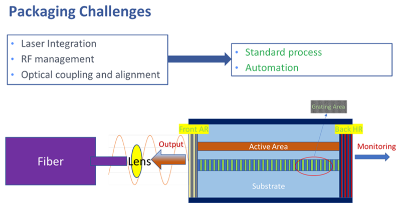
Figure 2. PIC Packaging Challenges
“We believe ultimately that consistent process control realized (through) less human contact with components and more automation will reduce process related failures. This requirement will be applied to the wafer level process as well as the photonic package level,” Zeng noted, adding that manufacturers are already responding. “We are consistently seeing monthly manufacturing yield and field quality performance improvements after we introduce more and more automation into packaging process. Tight and consistent screening for defects on the wafer level also helps to increase yield.”
“From what we have learned, more consistent process (steps) with less human handling errors results in higher quality of the photonic device. Co-packaged optics solutions will eventually help to meet those challenges. Co-packaged optics will integrate (the) ASIC and optics on the wafer level and dramatically reduce the integration steps required during packaging processes. Wafer level integration will aid quality because we will have many fewer discrete optical components; we will fully utilize current IC CMOS process standards to strictly control the building block process. In real application fields like in data centers, the number of pluggable devices will be dramatically reduced with deployment of the co-packaged optics switches,” he explained.
Despite the challenges being experienced as photonic integrated circuits (PICs) enter data center operations, the benefits of the PIC revolution such as reduced complexity, size and lower power consumption are greatly needed in data centers and along other infrastructure nexus points. Zeng reported that existing suppliers are stepping up and making changes, noting that, “…we are meeting with our suppliers intensively.” And while he expects that suppliers and manufacturers will continue to use proprietary ‘recipes’ for device fabrication, applying common standards like those used successfully in mainstream silicon and III-V device manufacturing will only speed what everyone hopes will be a successful transition to next generation high speed PIC transceivers.
“Volume demand is really the driving force for PIC, currently and for the foreseeable future. Big data centers will continue to play as the main force. The demands of Big Data are pushing this process; PIC (manufacturers) will respond to focus on (their) process development from the wafer level and prepare for another huge wave to come. The PIC era will arrive with denser optical electrical integration and more application and usage will be defined…The negatives we have experienced so far have impacted the scaled deployment within limited opening windows, but we will succeed. Manufacturers can be enablers of quicker, successful PIC device adoption by acting on our recommendations.”

Biography
Vincent Zeng is a Manufacturing Quality Engineer responsible for optics at Facebook, where he focuses on the management of optical products from qualification to deployments in Facebook’s Data Centres.
Prior to Facebook, Vincent Zeng was the Sr Quality Customer Manager at Brocade for optics and network equipment. He started his optical carrier at JDSU where he produced the first Telcordia Qualified AWG product.
Additional to that, he also spent a couple of years at semiconductor inspection equipment company-KLA Tencor. Vincent holds a doctoral degree in optical physics from Nankai University and Post-doctoral from Max-Planck Institute.

The Fraunhofer Heinrich Hertz Institut (HHI) is at the forefront of optochip and photonic integrated circuit (PIC) research. Executive Director Martin Schell provides insight into the Institut’s latest work with EMLs, EAMs and Mach-Zender modulators between 25 and 100 GBit/sec.
“Annual global IP traffic will reach 3.3 Zbyte per year by 2021…..” This forecast recently published by Cisco [1] looks like a huge market for transmitters, and receivers alike. On a closer inspection, however, optical component makers may get less excited. Thanks (or owing) to fantastic achievements on the high-speed performance of key components in recent years, single transmitter devices of fairly manageable design are capable today of delivering a modulation rate on the order of 50 Gb/s -100 Gb/s, and even beyond that when using more complex configurations.
Much of the IP traffic ends in data centers. Their typical architecture requires top-layer intra-center optical connections of 500 m to 2 km distance, and of up to 40-80 km between such facilities. Single-mode operation is of course compelling here. A simple calculation reveals that supporting a yearly data volume of 3.3 Zbyte, equivalent to an average data rate of about 8.3x1014 bit/s, would – theoretically – only need some 16,000 pieces of 50 Gb/s transmitter chips. With electro-absorption modulated lasers (EML), outlined below, these could be accommodated on a single wafer of 3-inch diameter, today’s standard size in InP technology.
In the end, the situation will not be as bad like that: One north-south bit may cause hundreds of east-west bits; the same bit may pass a couple of transmitters; and data centers should be equipped to handle peak traffic. A recent analysis of AIM Photonics Academy [2] concludes that for the data centers operated by the four giants: Amazon, Facebook, Google, and Microsoft, there will be a demand of approximately 22m pieces of 100 Gb/s transceivers per annum, translating into a lower 4-digit 3” wafer quantity. With 8 wafers grown in a single run, this would correspond to about 150 of 4-hour epitaxy runs per year for the base wafer.
Silicon Photonics (SiP) is being widely regarded as the technology of choice for implementing intra-datacenter transceivers using electro-optic modulators for data generation. Despite tremendous progress made during the past years, SiP is lacking the ability to make practical Si-based lasers, and in fact there is no solution in sight. Consequently, InP-based source lasers have to be incorporated, either by demanding hybrid assembly techniques or by a hetero-integration (e.g. wafer bonding) approach. While the former represents a serial manufacturing process the latter requires additional on-wafer InP processing which questions the economic advantages of the Si core technology. InP technology, on the other hand, provides the only material platform enabling true monolithic laser integration. This enables extremely efficient and small-footprint ultrahigh-bitrate transmitter chips. Whereas directly modulated DFB laser devices may be useful up to 25 Gb/s, EML structures are predestined for achieving much higher modulation rates and concomitantly higher transmission distances, thanks to the adjustability of zero and even negative modulation chirp.
Fraunhofer HHI has been pursuing an intense program to develop EMLs over almost a decade. A fairly simple design has been adopted that uses an identical layer structure for both the DFB source laser and the electro-absorption modulator (EAM). The active region consists of InGaAlAs quantum well layers. With etching an isolation trench between the DFB and the EAM section as a key manufacturing step on top of standard lasers, EMLs now have developed into reliable high-yield devices [3].
Typical performance parameters of HHI’s EML devices, featuring a 300 µm long DFB laser and an 80…120 µm long EAM section, are characterized by a static extinction ratio of > 20 dB at an EAM voltage swing of 2 V. A typical bias voltage is about -1 V, and below this point the chirp factor tends to become zero, and even negative when further shifting the bias towards larger negative values. The optical output power reaches some 5 dBm, generally limited by the fact that the DFB laser is not operated at optimum gain but is detuned to longer wavelengths to guarantee transparency of the electro-absorption modulator in the on-state.
To overcome that design-inherent issue, an optical booster amplifier has been added (Fig. 1) which provides output powers of >10 dBm. Even at 56 Gb/s the integrated amplifier does not affect the modulation behavior [4].
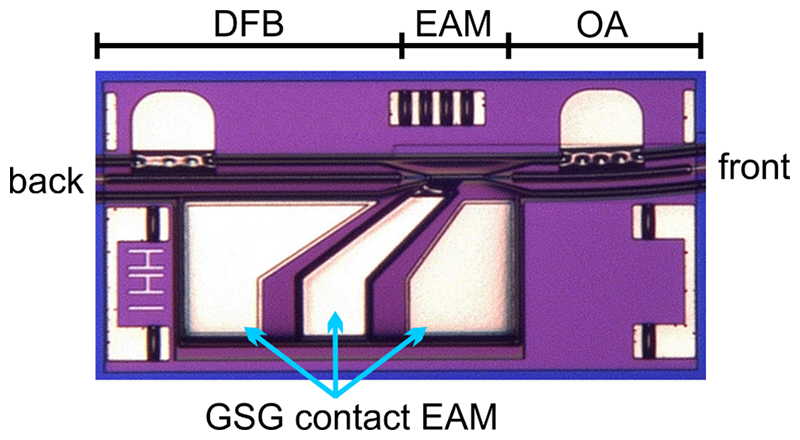
Figure 1: Top view of HHI’s EML chip comprising an optical amplifier (OA) section to boost the output power. All of the three sections (DFB, EAM, OA) are made of the same layer structure, with electrical separation between them achieved by isolation trenches. The optical output is tilted to help suppress optical back-reflection. RF feeding of the EAM part is supported by a Ground-Signal-Ground (GSG) transmission line.
Thanks to this upgrade, next-generation PON requirements (average modulated output power of min 9 dBm @10 Gb/s; 1577 nm) can readily be met. The modulation rate of 56 GBd is routinely achievable now. However, a baud rate of 100 GBd has been demonstrated very recently (Fig. 2) after introducing further design refinements.
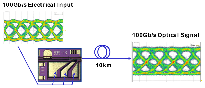
Figure 2: Demonstration of 100 Gb/s EML modulation capability (NRZ; λ=1300 nm; chip size: 420 µm x 320 µm)
Hence, a single-wavelength 100 G transmitter (on-off keying) may be implemented using a single tiny EML chip, provided suitable electrical drivers are available. In addition or instead, however, virtually all the common multiplex methods are applicable to efficiently accomplish even higher data rates and/or to exploit lower baud rates. 4- and 8-level Pulsed Amplitude Modulation (PAM) was successfully demonstrated on HHI’s EMLs. Using a proprietary SiGe based driver IC, clear 32 GBd PAM4 eye diagrams have been achieved at a driver power of 84 mW leading to a figure-of-merit of 1.3 pJ/bit (Fig. 3).
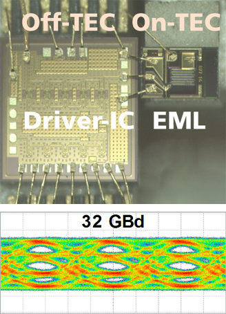
Figure 3: EML chip with co-packaged PAM4 driver IC designed at HHI. Power consumption of the driver IC is 84 mW (top); PAM4 eye diagram received at 32 GBd (bottom)
For space-division-multiplexed transmission, a serial dual-EML chip has been designed that comprises two EAMs in back-to-back configuration sharing the same DFB source laser between them [5]. Simultaneous modulation without mutual interference was demonstrated at 56 GBd (Fig. 4).
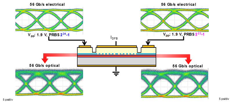
Figure 4: Dual-EML device sharing a common DFB source laser
For PAM4 schemes, a parallel 4-EML array was fabricated [6] which is capable of delivering an aggregated data rate of 224 Gb/s (4x 56 GBd). As a special feature, in this array the RF connections to the EAMs have been routed to the rear edge of the chip thus providing uniform RF driving conditions and concurrently facilitating packaging. While EMLs are now commonly used under TEC controlled conditions, typically at 40-50°C heat-sink temperature, uncooled operation (xx-90°) has been demonstrated recently.
Finally, generation of polarization-multiplexed signals has been shown. To this end, a photonic integrated circuit combines two EAM elements serially integrated with combiner/splitter-free polarization converters [7] and a DFB laser, as sketched in Fig. 5.

Figure 5: Image of a fabricated integrated Dual-Polarization EML device, consisting of (from left to right): a monitor photodiode (MD), a DFB laser diode emitting TE polarized light, two polarization converters, and two EAMs. The first polarization converter (45° PR) rotates the polarization by 45°, and the first EAM modulates the 50% of the laser light that remains TE-polarized. The following converter (90° PR) rotates the signal by 90° thus interchanging the TE and TM fractions. The second EAM modulates the light that was previously not modulated by the first EAM. The device was realized on HHI’s PIC foundry platform.
Respective chips have been fabricated on HHI’s generic PIC platform [8], and its functionality was successfully tested at 20 Gb/s per polarization state [9]. Such a chip measures only 3.2 mm x 0.2 mm. On a precursor chip without integrated laser, a total bit rate of 112 Gb/s was obtained using a baud rate of 28 GBd and PAM4 modulation [10]. By further inserting a phase shifter to modulate the optical phase between the TE- and TM-signal, a very compact transmitter for true 3-dimensional Stokes-vector modulation (SVM) could easily be implemented, delivering a bit rate corresponding to the threefold baud rate, and sixfold if additionally applying PAM4 signaling to each of the three channels. SVM represents a promising new direct modulate-and-detect technique, with a complexity and performance somewhere between direct and coherent transmission. This may have high potential for 100G access and metro networks –to make room for some more zettabytes to come.
An alternative to electro-absorption modulators is the Mach-Zehnder modulator (MZM). MZMs exploit the quantum–confined Stark effect which is quite efficient in InP based materials, particularly when using MQW structures. In comparison to EAMs, MZM devices build much longer (4… 8 mm). This is rewarded by higher static extinction ratios (> 25 dB), operation over a wider wavelength span (~ 50 nm), and eventually probably higher electro-optic bandwidth.
As with EMLs, there is long-standing experience and expertise with Mach-Zehnder modulators on InP at Fraunhofer HHI. Already in an early development stage, a traveling-wave electrode design has been introduced to boost the bandwidth. Meanwhile, a wide range of discrete as well as integrated modulator structures of high complexity (e. g. IQ modulators) have been developed. Some of them have been transferred into commercial products by partnering with companies. Among the more recent developments is an O-band MZM that has been monolithically integrated with a DFB laser. A key step further was the co-design of the electrical driver aimed at lowest power consumption. To this end, a 2-bit digital-to-analog converter was designed for optimum impedance matching. ICs were fabricated on a 0.13 µm SiGe BiCMOS foundry platform. Fig. 6 shows a transmitter subassembly combining this IC and the DFB-MZM PIC. Tested at 56 GBd, PAM4 modulation the overall power consumption including the laser, the modulator and the driver amounted to only 332 mW [11].
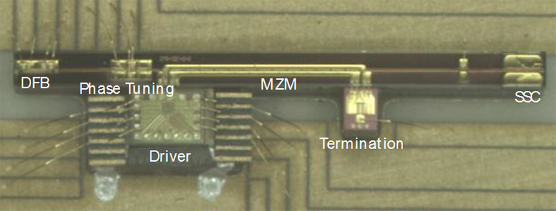
Figure 6: Co-packaged transmitter subassembly comprising the DFB-MZM chip, a 2-bit DAC driver and a load resistor. The unit was successfully tested at 56 GBd, PAM4 modulation requiring a total power consumption of only 332 mW
[1] Cisco White Paper” The Zettabyte Era: Trends and Analysis”, June 7, 2017
[2] AIM Photonics Academy; “Integrated Photonics Grand Challenges and Key Needs for 2018”, Webinar Dec 21, 2017
[3] M. Moehrle, H. Klein, C. Bornholdt, G. Przyrembel, A. Sigmund, W.-D. Molzow, U. Troppenz and H.-G. Bach, „InGaAlAs RW-based Electro-Absorption-Modulated DFB-Lasers for High Speed Applications”, SPIE Photonics Europe 2014, Brussels, invited paper 9134-44
[4] M. Theurer, G. Przyrembel, A. Sigmund, W. D. Molzow, U. Troppenz, M. Möhrle, „56 Gb/s L-band InGaAlAs ridge waveguide electro-absorption modulated laser with integrated SOA“, Phys. Stat. Sol. A213, 970-974, 2016
[5] M. Theurer, H. Zhang, Y. Wang, W. Chen, L. Zeng, U. Troppenz, G. Przyrembel, A. Sigmund, M. Moehrle, and M. Schell, “2 x 56 GB/s from a Double Side Electroabsorption Modulated DFB Laser and Application in Novel Optical PAM4 Generation”, J. Lightw. Techn., vol. 35, no. 4, pp. 706-710, 2017
[6] M. Theurer, M. Moehrle, U. Troppenz, H.-G. Bach, A. Sigmund, G. Przyrembel, M. Gruner, M. Schell, „4 x 56 Gb/s high output power electroabsorption modulated laser array with up to 7km Fibre Transmission in L-Band”, J. Lightw. Techn., vol. 36, no. 2, pp. 181-186, 2018
[7] M. Baier, F. M. Soares, M. Moehrle, N. Grote, M. Schell, “Highly fabrication tolerant polarization converter for generic photonic integration technology”, 28th IPRM (2016), paper MoC3-6
[8] F. M. Soares et al.,” High-Performance InP PIC Technology Development based on a Generic Photonic Integration Foundry”, OFC 2018, paper M3F.3 See also cover story of PIC Magazine, issue 4 (March 2017): “PICs at Fraunhofer HHI: Adding strength to InP photonic integration “
[9] M. Baier, F. M. Soares, T. Gaertner, A. Schoenau, M. Moehrle, M. Schell, “New Polarization Multiplexed Externally Modulated Laser PIC”, ECOC 2018, paper submitted
[10] M. Baier et al., “112 Gb/s PDM-PAM4 Generation and 80 km Transmission Using a Novel Monolithically Integrated Dual-Polarization Electro-Absorption Modulator InP PIC,” Proc. ECOC 2017, Th.1.C.4
[11] S. Lange et al., “Low Power Optical Transmitter with DFB-Laser Mach-Zehnder Modulator PIC and Co-Designed 2-Bit DAC Driver,” Proc. ECOC 2017, Th.1.C.5

EPIC is the industry association that promotes the sustainable development of organisations working in the field of photonics in Europe.
Our members encompass the entire value chain from LED lighting, Photovoltaic solar energy, Photonics Integrated Circuits, Optical components, Lasers, Sensors, Imaging, Displays, Projectors, Optic fibre, and other photonic related technologies.
VCSEL arrays have been employed recently to power cameras to improve 3D sensing features in smartphones. In the next generation, 3D sensing technology will enable accurate facial recognition, secure biometrics, gesture sensing, new gaming experiences and augmented reality. It is time for VCSELs to reach other applications related to metro networks, enabling higher capacities and reducing consumption and cost. By: Ana Gonzalez and Jose Pozo
The vertical-cavity surface-emitting laser, or VCSEL is a type of semiconductor laser diode with laser beam emission perpendicular from the top surface, contrary to conventional edge-emitting semiconductor lasers. VCSELs offer several advantages over Light Emitting Diode (LED) and Edge Emitting Laser (EEL) technology in terms of:
In the last decade, we have seen a continuous development of fibre optic networks for metropolitan applications. However, we are now facing a bottleneck in the transmission and the routing of data. Traditionally, the high-capacity systems targeting more than 100-Gb/s capacity per channel are exploiting high end optical transmitters based on distributed feedback (DFB) lasers and external Mach-Zehnder modulators (MZMs) to achieve high fidelity and high capacity links.
As the need for bandwidth capacity continues to grow exponentially, multi-Tb/s per second systems based on this high-end technology are becoming prohibitively expensive. However, due to the re-introduction of coherent detection technologies such as VCSEL sources in the last 10 years, many of the possible impairments, such as modulation related chirp, chromatic and polarization dependent dispersion and non-linearities can be compensated.
The EU funded PASSION project will develop new photonic technologies for supporting agile metro networks, enabling capacities of Tb/s per channel, 100 Tb/s per link and Pb/s per node over increased transport distances. To achieve this, PASSION will develop directly modulated WDM VCSEL sources for massive deployment, based on InP technology and working on single-mode operation. A large number of VCSELs will be integrated on a SiPh chip based on silicon-on-insulator (SOI) wafer processing and the light will be coupled directly from the VCSELs into the SOI PIC using a mirror in SOI to develop a novel 3D stacked modular design.
At the receiver side, PASSION will develop novel InP based coherent receiver arrays which handle polarization on chip making polarization handling off chip unnecessary. Finally, PASSION will develop a compact and cost-effective switching concept which can support the Pb/s capacities generated by the transceiver modules, using a combination of InP and SiPh PICs. Increased system flexibility and modularity is obtained by sliceable bandwidth/bitrate variable transceivers. The resulting solution will offer scalability, programmability and re-configurability using agile aggregation in spectrum, polarization and space dimensions.
“In PASSION, a new metro network infrastructure is envisioned, fitting the network operator roadmap and targeting at least a tenfold reduction in components energy consumption and footprint. “ Pierpaolo Boffi, coordinator of PASSION
Interview with QPOlens’ Jorge Sanchez
Jorge Sanchez is the Business Development Manager of QPOlens, a company specializing in the design and manufacture of plastic lenses for the control of light. QPO offers both custom-made lenses and standard lenses with high manufacturing volumes at very competitive prices for the following sectors: lighting, sensor, signalling, instrumentation, security, automotive, architecture, and light guides.
While Jorge plays a pivotal role in helping QPO grow its business, he was keen to emphasise that the core and spirit of the company is embodied in two other key persons: Carles Pizarro, CEO of the company who has more than 20 years of experience in the field of optical design-including plastic lens, and their CTO, Manel Espinola. Together, they have created a team that's a major driver in providing optical products with real added value.
According to Jorge, QPO’s approach is based on thermoplastic mould injection instead of thermosetting. With this process, queue time, misalignments and abrasions - the bottlenecks in a thermoset approach - are eliminated. Hence, with QPO’s proprietary technology and know-how, run time for operations and manufacturing costs are indeed optimized (Figure 1).
Jorge added that this approach is not disruptive and is very convenient in terms of manufacturing costs. Furthermore, it allows for flexible production to assemble the optical parts in the embedding process step in which many processes need to be adjusted to fit the production of complex, often free-form components (Figure 2). The adjustments include both component specific changes as well as standard process steps. Due to the need to produce large varieties of parts in small batches, process adjustments have to be both rapid and accurate - both of which can be achieved with the QPO approach.
In this sense, it is worth pointing out that this approach and the business model behind it has just received (April) the so-called “Seal of Excellence” (SoE) from the EC, being recommended for funding after the corresponding evaluation by an international panel of independent experts. “In this sense, we encourage photonics community investors to contact us since a capital increase is in process to automate the process and dimensionate batches runs in order to optimize the real time to market with a proven optimization costs for mass production,” Jorge said.
The best market/application to develop QPO
Currently, QPO has three main applications in the pipeline: datacomm applications (backbones); the other two concern lighting. The company is young with a novel technology, so the urgent need is to position the technology and show its added value. In all LED and automotive markets, QPO is carving out a niche position. The LED lighting in automotive can be divided into three main parts: lighting itself, comfort/economy and complimentary lighting, which is the most promising for QPO. In this regard, QPO is currently working on projecting lights that project to ground level in high-quality cars.
About the interviewer: Dr. Jose Pozo is Director of Technology and Innovation at EPIC
(European Photonics Industry Consortium). As EPIC’s CTO, he represents 380 companies active in the field of Photonics. His job consists of actively engaging with these companies and providing tools to strengthen their position in the supply chain, organizing 20 technology workshops per year, providing market intelligence, and finding B2B leads. He has a vision that, to a large extent, the future of optoelectronic manufacturing can take place in Europe and as part of that vision, he is actively involved in EU-funded pilot lines. He has a 20-year background in photonics technology, market knowledge, and is part of a large network within the industrial and academic photonics landscape.
About QPO Lenses
QPO Lenses specializes in the design and manufacturing of plastic lenses for light control. The manufacturing methods and automated lines can handle multi wafer runs with a flexible encapsulation system that overcomes the current challenge of manufacturing costs by a solution based on thermoplastics. This allows QPO to supply customized lenses as well as large volume manufacturing at competitive rates and to develop quality optical solutions for a wide range of sectors and applications: lighting, signage, sensors, architecture, light guides. www.qpolens.com
(Figure 1). Example of FoT emitter with its embedded and assembled optics made with thermoplastics
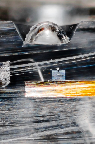
(Figure 2). Vertical analysis of a typical E-o device with the assembled optics in the embedded part of the process
Jose Pozo, Director of Technology and Innovation at EPIC, interviews Michael Geiselmann, Managing Director of LiGenTec
What is Ligentec?
LIGENTEC is a silicon nitride photonics foundry based in Switzerland. Our heritage is dispersion engineered, ultra low-loss, non-linear resonators used in Kerr combs, that came from the EPFL laboratory; LIGENTEC is a spin-off. The EPFL (ETH Lausanne) laboratory was developing integrated platforms with high quality factor resonators for nonlinear photonic applications such as frequency comb generation. These platforms started to attract a lot of interest for the use in a variety of applications, so we decided to investigate the possibility of scaling up the process to make it commercially available. This was made possible thanks to Dr. Michael Zervas, cofounder of LIGENTEC, that pooled his experience from Oerlikon, IBM and Intel and was able to bring both commercial and process knowhow.
LIGENTEC is now providing a complete low loss platform based on thick film stoichiometric LPCVD silicon nitride with a turnaround time of two months, which is 2-3 times faster than other foundries. The high confinement waveguides enable a decrease in chip size by a factor of four as bends can be as small as a few tens of micrometres. The complete platform includes a PDK with verified designs and its fully configured software environment.
What have been the main difficulties in going from the lab to the customer?
The PIC market has still low volume fabrication compared to CMOS. Working at low volumes and achieving customer specification requires a tight process control at wafer level. A student is happy if one chip works, but the customer wants every chip to work that he gets delivered. Furthermore, as the market is segmented, it has been necessary to determine what market needs we can fulfil, where they are and promote our services in these markets.
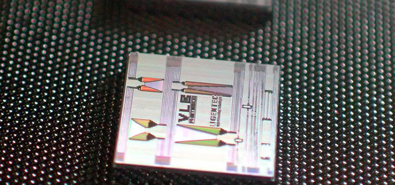
One of the issues in the integrated photonics industry is standardized testing. To solve the challenge, you mentioned testing at the wafer level. Do you think it would be desirable to work with the rest of the ecosystem or is it something that every foundry should solve by itself?
For process control, it's so fundamental to the business that it needs to be done in-house; for passive components process control is sufficient having established a statistical model. For other integration, like packaging, you could use outside partners. Functionalization of the final device could also be outsourced to someone with the required expertise who could serve several foundries.
Regarding your point about selecting markets, which markets do you think integrated photonics in general should focus on?
Our view is that there is a huge potential for future photonic chips serving new markets, away from the traditional telecom and datacom space.
For us, the one important new technology on the horizon is bio application and microscopy as they can benefit a lot from integrated photonics, for example going from a bulk to an integrated system or replacing fibre links with an optic chip. Here, silicon nitride has a great advantage because it provides transparency in the visible region. Other important potential new markets are in quantum, microwave photonics, LiDAR or neuromorphic computing that uses phase arrays. These markets all need hybrid integration in the next five years, to benefit from the best performance from different platforms, as there is no platform that can provide everything (low loss, active elements, transparency window). Then, especially for our technology, there are some niche markets, for example, in telecommunications in space and laser metrology market.
What about vertical integration, do you think you will need to move away from an application independent system?
We provide building blocks and a process design kit (PDK) with software packages that customers can use to create an application of choice. We focus on specialized integrated photonics and this is one of our key advantages compared with larger foundries, specialized in electronics, that are less willing to accept the change. Furthermore, electronics foundries are linked to the electronics cyclic market; this means that photonics can be reduced in fab priority as the market swings to the plus side, leading to product delays and cost increase (for photonics). In the segmented and lower volume PIC market compared to CMOS, the added value coming from specialising and focusing on all our resources to provide the single best process available and then working with similar solution providers (EDA, packaging, designs) in their focused areas.
What about the role of integrated photonics in medical applications?
Integration of all wavelength laser combinations on a chip will produce much smaller and more compact modules at a similar or cheaper cost. For example, a handheld device for sensing using a spectrometer with integrated photonics or point of care devices.
Finally, what applications will enable volume production silicon nitride devices?
High volume is definitely in sensing where you need a large transparency window as well as LiDAR, AI and 5G where you need to propagate higher powers than a few milliwatts or have long delay lines. These are promising future volume markets for silicon nitride.
What gasses are the most important?
There has to be a large demand for detecting them and ideally, they should be detectable without much additional effort in terms of absorption wavelength where laser sources are available, (e.g. methane) otherwise they won't generate volume production, although some gas detection could still become interesting for a niche market. Common gases are carbon monoxide, and CO2, methane, etc., which will require greater monitoring in future to contain exhaust emissions and air contamination.
EPIC environmental monitoring event
In response to Michael’s comments concerning gas detection, Jose commented that EPIC plans an environmental monitoring event on 15-16 October at the headquarters of Avantes, an EPIC member that expects in the next 2 to 3 years, that integrated photonics is going to bring about a big paradigm shift in the cost and size of spectrometers.
MARKETING
When you started, would you have appreciated more guidance about the marketing channels you deeded to address?
Definitely yes! One piece of advice I have is don't try it on your own: seek help from partners with market expertise. This is the good thing about EPIC because you can become integrated in the ecosystem and find a lot of information, such as market reports and talk to people with marketing knowhow.
A product doesn’t sell itself just because it's a good product: it needs to be marketed. Marketing is not just about making a nice advert; it's understanding the market, understanding the needs of the customer and your key selling points, which need to be included in the message. For example, we have a very fast turnaround time of two months, which is very important if the customer is proving a first prototype and doesn't want to wait 6 months. Another of our key selling points is that we produce silicon nitride circuits with a very low propagation loss, which is important if you need to buy a powerful laser and don't want to lose power in your circuitry.
You have to do your homework and build in marketing in the first stage of your business plan before you go out and communicate it. You have to know the market and the strengths all of your products and you have to be aware of the need to give different pitches to different kinds of people.
ADVICE TO YOUNG ENTREPENEURS
Finally what advice would you give to young entrepreneurs wanting to start their own business?
Don't try to do everything on your own: listen to other people, attend courses and don't think that you know everything. Join EPIC and other networks so you can benefit from the wide range of experience and know how.
PIXAPP Photonic Integrated Circuit (PIC) Assembly and Packaging Pilot line.
As a final note, Jose wanted to draw readers' attention to PIXAPP, which aims to be inclusive and involve as many key players as possible by creating an interest group to help this pilot line. For more information, please contact Ana Gonzalez, EPIC R&D Manager: ana.gonzalez@epic-assoc.com

EPIC Round Table on LiDAR Technology for Defence took place on 8 February in Paris. The event was held in conjunction with OPTRO. Light detection and ranging (LiDAR) systems are enabling the examination, detection, and mapping of objects easier, faster and with equal or higher resolution than conventional methods. They are one of the main enablers of the upcoming autonomous car industry, and are already in used in defence, security and aviation/aerospace applications. It is in those applications where the high resolution enabled by LiDAR system makes them particularly good for collecting enough detail to identify targets, such as tanks. LiDAR is proving to be increasingly useful in the autonomy of robots, allowing the computers that control them to produce digital maps of the surrounding area and obstacles. This kind of autonomy is useful in both UAVs (unmanned aerial vehicles) and specific task autonomous robotics such as bomb disposal units. The purpose of this round table was to discuss the still unmet needs for 3D sensing in the security, defense and aerospace sectors as well as strategizing to achieve the further adoption of next generation miniaturized, lower cost or higher integration LiDAR systems. The invited keynote speaker was Nikolaus Schmitt, Senior Expert Optronic Systems at Airbus. There were 11 presentations and 27 participants from 10 countries.

EPIC Meeting on Testing of Optoelectronics took place on 15-16 February in Belfast. The event was hosted by Yelo. The need to improve, speed-up, and reduce cost of packaging and assembly of optoelectronic devices is in constant debate. But as production numbers increase, another need is also attracting more attention: Testing. In many optoelectronic devices (Silicon Photonics, InP PICs, VCSELs, LEDs, DFB lasers, etc.) testing is performed at wafer level, at die level, as well as in a packaged device or module, and requires the combination of more conventional electrical probing and optical measurements, either with probing fibres or by means of near field / far field beam analysers. Similar to packaging, testing starts at design level and ends with automated test machines. There were 24 participants from all over the world including: Japan, USA and Europe, discussing requirements of probing techniques, handling, test procedures and needs for dedicated modular instrumentation, as well as finding combined solutions by means of collaboration between top companies and R&D centres in testing methodologies. The meeting concluded with a whisky tasting!


EPIC events are renowned for excellent networking, creating new connections and strengthening existing ties. Connecting EPIC members means building trust within the photonics industry, its leaders and experts.
EPIC Networking Reception at OFC took place on 13 March on the rooftop of the Hard Rock Hotel in San Diego. EPIC gathered 120 EPIC members and VIPs of the photonics industry in an evening with live music and excellent Mexican cuisine. With the perfect setting to talk business with key representatives of the photonics industry, the feedback of the attendees was extremely positive once again.
EPIC VIP Party at PIC International took place on 9 April in Brussels. 60 EPIC members, industry leaders, and decision makers from the photonics integrated circuits industry were together in the heart of Brussels to enjoy a fruitful evening of networking.
EPIC Meeting on Automation Tools for Packaging and Testing was scheduled to take place on 22-23 May in Karlsruhe. (Look for an update in a future edition of PIC Magazine.) The purpose of the meeting is to bring together equipment manufacturers and companies investing or interested in the further automation of their high precision manufacturing and testing lines, to discuss the production of optoelectronic components and modules (Silicon Photonics, PICs, AOC, VCSEL, Laser Diode, WLP, 2.5D/3D IC, TSV, TCB, Fan-out/EWLP,…) and to identify bottlenecks in process automation for any industry (HPLD manufacturing, fiber-optics and opto-electronics, medical technology, security and military applications, R&D, telecommunications, and others) and volume demand. The EPIC Meeting on Automation Tools for Packaging and Testing will have the participation of EPIC members such as Jenoptik, FiconTEC, VTT, imec, Yelo, IRSweep, Nanosbribe, CESEM, Xeryon, TNO, QPO lenses, Aifotec…
Upcoming PIC related EPIC events:
24 September EPIC VIP Party at The ECOC Exhibition, Rome, Italy
15-16 November EPIC Meeting on Environmental Monitoring at Avantes, Apeldoorn, The Netherlands
Find out about upcoming EPIC events on www.epic-assoc.com/epic-events

A variety of silicon-based technologies have given rise to expansive opportunities for photonic integrated circuits. While silicon enabled many photonic product developments, there is no one-size-fits-all approach; hybrid modules and the benefits of III-V technologies can resolve issues that elude all-silicon designs. By: Prof. Sasan Fathpour, College of Optics and Photonics (CREOL), University of Central Florida
Photonic integrated circuits (PICs) owes its birth to III-V compound semiconductors, and the traditional field of optoelectronics that has been built around these versatile materials since the 1960s. Since the 1980s, though, silicon photonics has slowly but surely been pursued as an alternative platform. Realized primarily through silicon-on-insulator (SOI) wafers, the argued advantages of silicon over III-V PICs have been much more compact optical waveguides with lower optical propagation loss, better processing yield, lower cost and compatibility with silicon foundry processing. Integration with CMOS electronics is another advantage, historically, but it is much less critical these days, as the trend is to have photonics and electronics on separate chips. Nonetheless, it was clear from the get-go that there is no “pure silicon” photonics, since other materials are inevitably required for a variety of functionalities that cannot be easily achieved in silicon. Some of the widely known shortcomings of silicon for integrated photonics are: (a) Lack of light generation [due to silicon’s indirect bandgap]; (b) Negligible photodetection in the telecom range and above [due to silicon’s bandgap energy]; (c) Lack of electrooptic or Pockels effect and second-order optical nonlinearity [due to silicon’s centrosymmetric crystal symmetry]; (d) Inefficient third-order optical nonlinearity below 2.2 μm [due to nonlinear absorptions]; (e) Loss of the buried oxide (BOX) layer of SOI in the mid-infrared wavelengths [1].
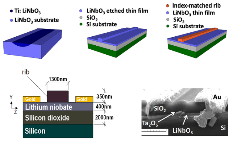
Addressing the former two shortcomings was more critical in the development of the silicon photonics technology for its prime application: datacom. Integrating thin layers of germanium in waveguide photodetector configuration has long been a standard procedure, hence group-IV photonics has been a common term for the technology too. Meanwhile, despite tremendous amount of efforts, dependable silicon-based lasers remain elusive to date. Instead and despite certain downsides, various methods for hybrid integration of III-V lasers have been successfully developed and are widely in use in commercial transceiver chips. Given this, maybe “groups III-to-V photonics” is semantically a more accurate descriptive name for silicon photonics.
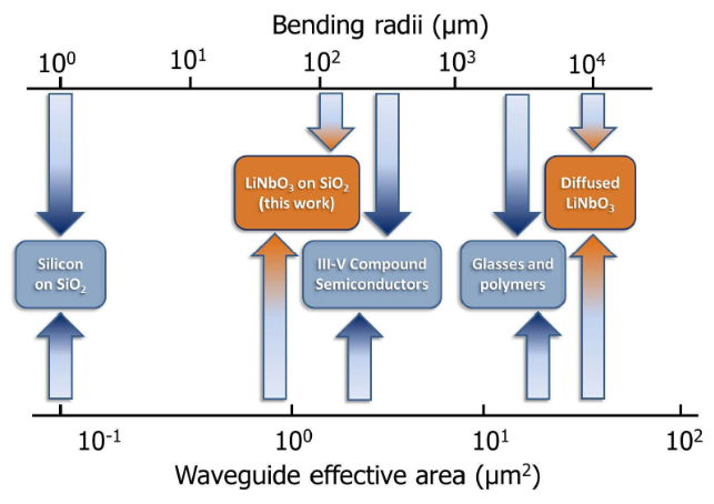
The mentioned lack of ‘true’ electrooptic effect in silicon has been circumvented by the less attractive phenomenon of plasma dispersion effect, in which the free-carrier density is modulated electronically, usually via a p-n junction diode straddling SOI waveguides. Reasonably high data transmission rates are routinely achieved, but silicon modulators inherently suffer from low extinction ratios or modulation depths, limited to a few dB, particularly at the high data rates of interest. Such low performance may be acceptable for current datacom applications, where fiber-optic links with on-off keying reaching to a maximum of a couple kilometers are targeted. However, if it is intended to expand the realm of silicon photonics to longer links and/or more advanced modulation formats, the low extinction ratio of modulators based on plasma dispersion effect will become a bottleneck for system performance.
The best-known phenomenon and material for optical modulation is the electrooptic or Pockels effect in lithium niobate. Dominating the long-haul communication market for decades, lithium niobate Mach-Zehnder modulators boast low loss, remarkably high modulation depths of higher than 20 dB and modulation bandwidths of up to 100 GHz. The challenge for this technology is that the devices are bulky, power-hungry, expensive and do not lend themselves easily for integration of multiple devices. The root problem is the common waveguide formation techniques of proton exchange or titanium indiffusion, resulting in low-index-contrast waveguides and, in turn, leading to large drive voltages, length and bending radii. Therefore, a high-contrast and low-loss lithium niobate waveguide technology is desirable. In addition, if the lithium niobate photonics technology is merged with silicon photonics at the back end of line (BEOL) portion of foundry fabrication, it could be game-changing.
To this end, the author’s group at CREOL has been working on developing such a technology for several years. We reported the first lithium niobate on silicon wafers, waveguides and modulators in 2013 [2]. The in-house fabrication process actually resembles the SmartCut method of SOI and involves ion implantation of bulk lithium niobate wafers, bonded to oxidized silicon wafers, followed by thermal slicing to leave a thin film (200 to 600 nm) of lithium niobate on a silicon dioxide insulating layer, serving as the bottom cladding of the waveguides.
In principle, dry etching of lithium niobate can be used for ridge formation and lateral optical confinement. In practice and to avoid the challenges of etching lithium niobate, we have been typically relying on the simpler and more reliable solution of rib-loading the thin films. The choice of the rib material is not that critical, as long as its refractive index roughly matches that of lithium niobate, can provide low loss and it is easy to process. Based on this maturing waveguide platform and in a series of research papers [2-4], we have so far successfully reported the first lithium niobate microring and Mach-Zehnder modulators on silicon. The latest generation of Mach-Zehnder modulators possess a 3-dB bandwidth of 33 GHz, low half-wave voltage length product of 3.1 V.cm at DC and less than 6.5 V.cm up to 50 GHz. Notable is the high extinction ratio of 18 to 20 dB in the devices, on par with commercial lithium niobate devices and much higher than the mentioned plasma dispersion effect in silicon. Optimized designs confirm that devices with up to 100 GHz bandwidth are attainable.
Encouraged by the above promising results, our research team has established a spin-off company, Partow Technologies (http://www.partow-tech.com/). The company has already been marketing the lithium niobate on silicon wafers for three years for photonic and non-photonic applications and is progressing towards commercializing thin-film modulators and other photonic circuits on the heterogeneous wafers.
The previously mentioned issues pertaining to light generation, detection and modulation are not the only shortcomings of silicon photonics. For example, other issues arise for nonlinear and mid-infrared applications. Although these applications may not have a large market yet or the solutions may not be ready for commercialization, they may become important in future developments.
Lack of electrooptic or Pockels effect in silicon is tightly related to the lack of second-order optical nonlinearity. The associated nonlinear phenomena have potential applications in light sources at lower (e.g., via second-harmonic generation) or higher (e.g., via difference-frequency generation) wavelengths than a pump source’s, self-referencing in optical combs, quantum photonics at telecom wavelengths, and more. Readily, the discussed lithium niobate platform can be exploited for such nonlinear frequency conversion applications. We have accordingly reported second-harmonic generation and entangled photon generation. Typically, phase-matching techniques are required for efficient conversion. We have applied the conventional period poling, as well as a novel method, dubbed mode-shape modulation, to address this requirement [5, 6].
Third-order optical nonlinearities also have a whole host of applications, for example four-wave mixing and continuum generation. Silicon has high third-order nonlinearity but at wavelengths below the two-photon bandgap of ~ 2.2 μm, the Kerr and Raman nonlinear effects are significantly hampered by nonlinear absorptions. Although carrier sweep-out techniques alleviate the issue to a certain extent, for the most part researchers have moved to other highly nonlinear materials such as silicon nitride and chalcogenide glass to form waveguides for nonlinear applications on silicon [1, 7].
An emerging research area is the quest for simultaneously integrating all these materials on the same chips. For example, it is key to “co-integrate” cascaded waveguides with second- and third-order nonlinearities for frequency-stabilized optical comb generation. Chalcogenide or silicon nitride waveguides can be exploited to achieve octave-spanning supercontinuum generation (SCG), while second-harmonic generation in lithium niobate can be used for stabilization by f-to-2f carrier-envelope offset (CEO) locking. We have recently reported progress towards such multimaterial integration, in which light enters a top-layer chalcogenide waveguide and then it is directed by adiabatic tapers into a lithium niobate underneath waveguide [8].
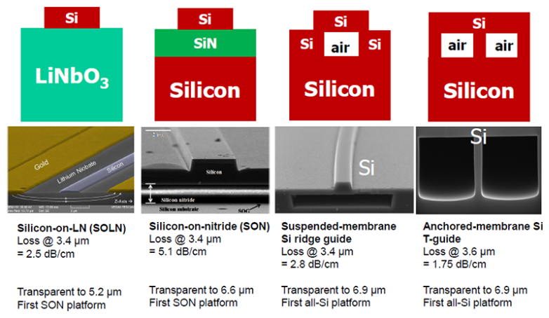
Last but not least, mid-infrared wavelengths (~ 3 to 5 μm) could be another up-and-coming application of silicon photonics. The challenge here is that the BOX bottom clad layer of the standard SOI waveguides is lossy at certain bands within this wavelength range. In order to eliminate oxide from silicon waveguide structures, our team reported the first silicon-on-nitride waveguides in 2013 [9]. We later reported two types of all-silicon air-clad suspended- and anchored-membrane waveguides [10, 11], which do not rely on wet etching the BOX layer. Rather, mechanically robust mid-infrared waveguides are achieved by trench formation in bulk silicon, bonded to an SOI die followed by substrate removal.
Given the limited space, the above focuses on the works demonstrated in the author’s lab. But they are just examples of a trend in moving away from the standard silicon photonics technology based on SOI waveguides/III-V lasers/germanium detectors. Many other teams around the globe are working on similar or other platforms, all aimed at increasing the performance of existing functionalities or at adding new functionalities. The common theme of all of them is heterogeneous integration of multiple materials for various devices and circuit segments on the same chip, preferably on silicon substrates. It is interesting that the alternative to such heterogeneous approaches is perhaps nothing but III-V PICs, provided that their mentioned issues of compactness, low loss, processing yield and cost are solved.
More reading
[1] S. Fathpour, "Emerging Heterogeneous Integrated Photonic Platforms on Silicon," Nanophotonics, vol. 4, pp.143-164, 2015 (INVITED).
[2] P. Rabiei, J. Ma, S. Khan, J. Chiles, and S. Fathpour, "Heterogeneous Lithium Niobate Photonics on Silicon Substrates," Optics Express, vol. 23, pp. 25573-25581, 2013.
[3] A. Rao, A. Pail, J. Chiles, M. Malinowski, S. Novak, K.A. Richardson, P. Rabiei, and S. Fathpour, "Heterogeneous Microring and Mach-Zehnder Modulators Based on Lithium Niobate and Chalcogenide Glasses on Silicon," Optics Express, vol. 23, p. 22746-22752, 2015.
[4] A. Rao, A. Patil, P. Rabiei, A. Honardoost, R. DeSalvo, A. Paolella, and S. Fathpour, "High-Performance and Linear Thin-Film Lithium Niobate Mach–Zehnder Modulators on Silicon up to 50 GHz," Optics Letters, vol. 41, pp. 5700–5703, 2016.
[5] A. Rao, M. Malinowski, A. Honardoost, J. R. Talukder, P. Rabiei, P. J. Delfyett, and S. Fathpour, "Second-Harmonic Generation in Periodically-Poled Thin Film Lithium Niobate Wafer-Bonded on Silicon," Optics Express, vol. 24, p. 29941, 2016.
[6] A. Rao, J. Chiles, S. Khan, S. Toroghi, M. Malinowski, G. F. Camacho-Gonzalez, and S. Fathpour, "Second-Harmonic Generation in Single-Mode Integrated Waveguides Based on Mode-Shape Modulation," Applied Physics Letters, vol. 110, p. 111109, 2017.
[7] J. Chiles, M. Malinowski, A. Rao, S. Novak, K.A. Richardson, and S. Fathpour, "Low-loss, Submicron Chalcogenide Integrated Photonics with Chlorine Plasma Etching," Applied Physics Letters, vol. 106, p. 111110, 2015.
[8] A. Honardoost, G. F. Camacho Gonzalez, S. Khan, M. Malinowski, A. Rao, J.-E. Tremblay, A. Yadav, K. Richardson, M. C. Wu, and S. Fathpour, “Cascaded Integration of Optical Waveguides with Third-Order Nonlinearity with Lithium Niobate Waveguides on Silicon Substrates,” IEEE Photonics Journal, ACCEPTED.
[9] S. Khan, J. Chiles, J. Ma and S. Fathpour, "Silicon-on-Nitride Waveguides for Mid- and Near-infrared Integrated Photonics," Applied Physics Letters, 102, pp.121104, 2013.
[10] J. Chiles, S. Khan, J. Ma and S. Fathpour, "High-Contrast, All-Silicon Waveguiding Platform for Ultra-Broadband Mid-Infrared Photonics," Applied Physics Letters, vol. 103, p. 151106, 2013.
[11] J. Chiles and S. Fathpour, "Demonstration of Ultra-Broadband Single-Mode and Single-Polarization Operation in T-Guides," Optics Letters, vol. 41, pp. 3836-3839, August 2016.

Rapid growth has characterized the expansive trajectory of Technobis, a company that began creating optical fibre sensing technologies in 2006. The company integrated PIC-based solutions seven years ago, which helped Technobis to rapidly expand with a focus on high performance markets across defense, aerospace, automotive and other premium markets. By: Rolf Evenblij, Program Manager, Technobis Fibre Technologies

Technobis has developed and provided fibre sensing systems since 2006 for many applications and environments. The company started with free-space optics, but for the last 7 years has utilized photonic integrated circuit (PIC) technology. Technobis subsequently introduced sensing solutions providing up to sub-femtometer wavelength shift detection resolutions, more than thousand FBG sensors in an optical fiber, sub-nanometer displacement sensing resolution and sampling rates up to 20 Mhz. Using miniature and high-performance acquisition and control electronics, combined with compatible PIC packages has enabled the company to create multi-parameter fiber sensing solutions.
The Technobis Fibre Technologies Gator product line is based on a next-generation Fibre Bragg Grating (FBG) metrology system that utilizes integrated photonics technology.
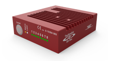
Throughout the years that Technobis has been active in this new technology field, many chips have been produced with a large number of different optical functions in different designs and configurations. These chips have been produced on multiple material platforms, each having its advantages, have been combined in order to achieve synergistic capabilities. Indium Phosphide (InP) supports both passive (waveguides, spectrometers) and active functions (light sources, lasers). Silicon on Insulator (SOI) has provided support for passive functions, but CMOS compatible and Silicium Nitride (Si3N4) has proven useful as a low-loss dielectric waveguide technology.
Technobis’ adoption of PIC-based technologies has enabled the company to participate in 30 multi-project wafer runs, including dedicated full-wafer runs, over 80 designs, resulting in more than 4,000 chips produced. After launching serial production of the Gator series in variants for channel multiplexing, optical references for long term stability, an integrated CPU for autonomous, wireless operation and data storage, not to mention the Chiroptera for high resolution displacement sensing, it is our belief that Technobis can rightfully claim to be a true frontrunner company in the world that is able to develop and supply (fiber) sensing systems based on integrated photonics. The PIC based platform brings the most accurate interrogators, solid state, high speed, high sensor count, and low power systems, combined with unmatched system pricing.
Technobis invested significantly in the development of fiber optic sensing systems based on integrated photonics and by doing so has achieved technology readiness levels for demanding market sectors. PIC technology proves enabling and brings significant advantages in critical sensing performance areas including resolution, speed and sensor multiplexing, as well as environmental endurance, which benefits high-tech industry, aeronautics, space. Its reliability (solid state, thermally and mechanically stable,) has also enabled Technobis to offer highly successful products. PIC advantages, together with the demonstrated capacity from Technobis to bring fiber optic sensing technology to the market, has convinced large companies in aerospace, space, and other high-tech industries such as biomedical applications, to regard this as a leap forward for applications in demanding environments where size, weight, reliability, cost and other factors are key requirements; conventional systems simply do not apply anymore. Many reliability tests and experiments were performed in order to demonstrate the maturity of the company’s technology, such as flight tests in large passenger aircraft, helicopters, civil and military vehicles under harsh conditions. Company products have also succeeded in passing radiation testing on bare dies and package systems.

The future for PIC based systems, and in particular for sensing applications, is huge and expanding. Based on what has been done so far, work at Technobis and companies like ours barely scratch the surface of what is possible. The PIC based development platform allows complex optical systems on just a few square millimeters, while packaging innovations make PICs work in stringent environments. As it explores and develops the potential of fibre-based optical sensing, the core optical fiber technology appears to demonstrate an increasingly number of sensing capabilities almost on a daily basis.
For PIC technology in general, one of the tendencies in order to consolidate new technologies is standardization as a means to reduce costs and improve efficiency in the supply chain. Generic processing is one of the ambitions for integrated photonics in order to reach this state. The advantages we expect to see in this evolution are reduced costs and lead-time in the supply of PIC based components. A well balanced interaction capability on a technical level within the supply chain is imperative for companies that want to reach the sky.
Current challenges for Technobis relate to ramp-up production capabilities and resources. Where comfortable product series volumes up to hundreds of units a year seemed sufficient in the past for conventional systems, this has in fact turned into a need for thousands units a year. This calls for significant upscaling of manufacturing capabilities and yield improvements. It requires awareness throughout the whole supply chain; the whole PIC ecosystem needs to ramp up in order to allow the technology to rise to achieving its vast mature technology potential. Technobis believes the only way to achieve this is by collaboration and helping to grow the number of applications for sensing and data/telecom. This means dissemination of knowledge and awareness in proper designing and packaging PIC-based systems, ideas that extend to partners and indeed, even to potential competitors in order to ensure a reliable supply chain and the long-term growth of the PIC industry. In practice, this translates into increasing the number of designs and simulations, more wafer runs, intensifying test and analysis of chips, upscaling packaging capabilities through development of test equipment, tooling, assembly automation, etc.
With Tipps (Technobis Integrated Photonics Packaging Services), Technobis recently launched its latest expansion, bringing into service large additional clean room and office space for volume packaging and assembly activities. The expansion comes with dedicated automated packaging equipment for testing products, die bonding, wire bonding, fiber alignment, etc. Technobis is a full-blown development and integrator company that is capable of realizing commercial PIC based products. Its strength is its practical approach to needs and capabilities that surpass what some see as technical boundaries; Technobis challenges fundamental limits. Tracking and pursuing opportunities combined with the ability to translate them in practical usage enables Technobis to succeed.
To recognise and highlight key industry achievements in advancing photonic integration through platform development, manufacturing, design, packaging and device characterisation, PIC Magazine host its 2nd PIC Awards programme. With nominations and voting taking place online and presentations made at the PIC International 2018 networking dinner on the evening of April 10th in Brussels, the awards put the spotlight on innovation. The awards programme is dedicated to celebrating leading lights in the industry.

Lifetime PIC Achievement
Professor Roel Baets
Individual Awards
Roel Baets (Professor) received an MSc degree in Electrical Engineering from Ghent University in 1980 and a second MSc degree from Stanford University in 1981. He received a PhD degree from Ghent University in 1984. From 1984 till 1989 he held a postdoctoral position at IMEC (with detachment to Ghent University). Since 1989 he has been a professor in the Faculty of Engineering and Architecture at UGent where he founded the Photonics Research Group. Roel Baets has made contributions to research on photonic integrated circuits, both in III-V semiconductors and in silicon. In 2006 he founded ePIXfab, the first Multi-Project-Wafer service for silicon photonics. Since then ePIXfab has evolved to be the European Silicon Photonics Alliance. He leads the Photonics Research Group at Ghent University. Roel Baets is also director of the multidisciplinary Center for Nano- and Biophotonics (NB Photonics) at UGent, founded in 2010. He was co-founder of the interuniversity UGent-VUB MSc programme in Photonics and of the European MSc programme in Photonics. Roel Baets is a grant holder of the Methusalem programme of the Flemish government and of the European Research Council (ERC advanced grant). He is a Fellow of the IEEE, of the European Optical Society (EOS) and of the Optical Society of America (OSA) He is also a member of the Royal Flemish Academy of Belgium.
NOMINEES
Ronan Burgess, Andy Carter, Fred Kish, John E. Bowers

PIC Entrepreneur and Business Leader
Dr Michael Lebby
Individual Awards
Dr. Michael S. Lebby has been the Chief Executive Officer of Lightwave Logic, Inc. since May 1, 2017. Dr. Lebby serves as an Advisor at Redfern Integrated Optics, Inc. Dr. Lebby served as the Chief Technology Officer and General Manager of Translucent at Silex Systems Ltd. Dr. Lebby Founded Ignis Optics, Inc. since 2001 and served as its President and Chief Executive Officer. He served as the President and Chief Executive Officer of Optoelectronics Industry Development Association (OIDA)., since 2006. He has more than 20 years of experience in the field of optical communications. In 1985, he joined ATT Bell Laboratories. He joined Motorola's Phoenix Corporate Research Laboratory, where he served as its RD Business Technology Development Manager in 1997. Dr. Lebby served as Head of Translucent at Silex Systems Ltd. From 1990 to 1998, he served as an RD section head of Motorola's OPTOBUS program. He was a member of ATT Bell Labs and British Ministry of Defense Photonic research efforts, where he concentrated on InP and GaAs OEIC's. After a year at AMP as a member of the Global Optoelectronics Division's management team, Dr. Lebby joined Intel Capital as a Corporate Investor. His career has spanned all aspects of the optoelectronics business, ranging from research and development, to sales, marketing and investing. Dr. Lebby is internationally recognized as a technologist, leader and market expert in optics and photonics. Dr. Lebby's reputation in the field of optoelectronics is widely recognized with wide-ranging experience across many key areas including: Intel Capital Optoelectronics team, ATT Bell Labs and Motorola photonics research, Oclaro as well as an Entrepreneur with his own venture backed fiber optics start-ups. He headed the Optoelectronics Industry Development Association (OIDA), the premier networking trade association for business and scientific professionals in the optical space based in Washington, DC. Dr. Lebby has testified on behalf of the optoelectronics industry on Capitol Hill and brought the industry together on key issues. In 2015, Dr. Lebby completed a set of industry roadmaps for integrated photonics technologies over the next decade as part of the Federally funded IMI (Institute of Manufacturing Innovation) competition. With over 200 USPTO issued utility patents (and over 395 including national and international derivatives), Dr. Lebby is considered to be one of the most prolific inventors in the field of optoelectronics. He is also a Fellow and member of the Institute of Electrical and Electronics Engineers (IEEE) and the Optical Society of America (OSA). He has been Executive Director of OIDA since 2005. He serves as Director of Optoelectronics Industry Development Association. He serves as an Independent Director of IntexyS Photonics SA. He serves as Member of Technical Advisory Board at Translucent Inc. He served as Director of Intel. He served as Director of AMP/Tyco. He served as Director of Redfern Integrated Optics, Inc., since June 6, 2007. He has been an Director of Lightwave Logic, Inc. since May 1, 2017 and served as its Independent Director August 26, 2015 until April 1, 2017. Dr. Lebby holds more than 200 US patents in optoelectronics. He is a Fellow member of IEEE and OSA. Dr. Lebby was awarded the degree of Doctor of Engineering in 2004 as well as PhD in 1987 and an MBA in 1985 from the University of Bradford in the United Kingdom.
NOMINEES
Fang Wu, Bill Ring, Pascual Munoz / Jose Capmany, Hans van den Vlekkert, Tim Jenks, Radha Nagarajan

PIC Technologist
Bill Ring
Individual Awards
Bill Ring is currently a Senior VP at Poet Technologies where his work encompasses both III-V devices and dielectric technology. The major focus of the Dielectric waveguide development is currently on the introduction of Poet’s Optical Interposer Platform utilizing a low loss dielectric waveguide that is deposited and compatible with current CMOS processes. Previously, Bill was CEO of BB Photonics Inc., a start up developing uncooled 100GbE receivers using InP PICs with embedded dielectric waveguides. This was sold to Poet Technologies in June 2016. From 2010 to 2014, Bill was involved in the due diligence and purchase of Solar Systems Pty Ltd, an Australia concentrated photovoltaic company, where he subsequently held the roles of GM and then Chief Technology Officer for the company. Prior to this, he had started a consulting company in 2005 that worked with several fortune 500 companies and many start-up companies in the areas of defense, optoelectronic components and datacenter optical devices. During this period he also managed workshops for the USA based Optoelectronic Industry Development Association (OIDA) from 2005 to 2009. Before 2005 Bill held positions at Tyco Electronics, as Director of Operations and Director of development for devices and transceivers. Before joining Tyco, he was a Principle Engineer at Hewlett Packard (HP) and responsible for the design and development of 1310nm FP, 1480nm pump and DFB lasers for HP’s fiber optics group. In 1995 he introduced the first strained MQW laser into production at HP's UK facility that was later deployed in HP’s 1300nm SFF/SFP transceivers. Bill Holds a PhD from Surrey University in III-V light emitting devices, which showed that Intervalence Band Absorption (IVBA) was not the dominant loss mechanism in long wavelength lasers.
NOMINEES
Peter O’ Brien

PIC Hero
BRIGHT Photonics & NAZCA
Company Awards
BRIGHT Photonics is the first commercial PIC design house and behind the first commercial modules for technology transparent design of PIC components like AWGs and interconnects. In 2017 BRIGHT launched “NAZCA Design”. A state-of-the art free and open source PIC design tool for mask layout and more. It highly stimulates open access and open innovation for commercial and research projects. NAZCA turns out to be a game changer. The photonics community is adopting it rapidly as the tool of preference for its quality, efficiency and flexibility. While sharing PIC design for free with the community, the core business of BRIGHT Photonics remains quality driven commercial product development support for PIC based applications.
NOMINEES
Christian Koos, KIT

Advances in Photonics Integration
Ayar Labs
Company Awards
Our mission is to cut the amount of energy used in computing in half, by removing bottlenecks in moving data. We help companies keep up with skyrocketing volumes of data by miniaturizing fiber optic transceivers and making them in standard silicon chips, replacing copper interconnects and bringing the super-high bandwidths and low energy use of optical communications inside computers.
NOMINEES
VPIphotonics GmbH, LioniX International, VLC Photonics, FP7 PhoxTroT Consortium, IHP, Sicoya, Multiphoton Optics

Advances in PIC Manufacturing
LioniX International
Company Awards
LioniX International has been established in April 2016, and has acquired LioniX, Satrax, XiO Photonics and OctroliX B.V. The focus of LioniX International is on PIC enabled modules based on its proprietary waveguide technology (TriPleX™), in addition to microfluidics, optofluidics and MEMS. The acquisition of the aforementioned companies creates a vertical integrated company that delivers a complete solutions: from initial design through volume manufacturing of products. In addition, LioniX International has entered into strategic collaborations with partners in South Korea, to provide high-volume manufacturing of chips and assemblies, thereby enabling a seamless transition from prototype to high-volume manufacturing.
NOMINEES
VLC Photonics, Physik Instrumente, ficonTEC, Luxtera, Intel, Neophotonics, Juniper, Infinera, IQE

PIC Platforms
Ligentec
Company Awards
LiGenTec SA is a company located at EPFL innovation park in Switzerland and an expert in offering silicon nitride thickness above 600nm maintaining very low waveguide propagation loss.The main application areas include integrated quantum photonics, high Q-filters, supercontinuum generation, pulse generation, spectroscopy, bio-sensing and microwave photonics.With its silicon nitride chips LIGENTEC enables products based on integrated photonics for fabless companies and research institutions to be able to work with silicon nitride.
NOMINEES
GCS, Oclaro, Lumentum, IBM, Cisco
|
Associations |
||

|
EPIC |
|

|
||

|
PIC International 2018 |
|
|
Component |
||

|
DenseLight |
|

|
POET Technologies |
|
|
Design Services |
||

|
PhoeniX Software |
|

|
VLC Photonics |
|
|
Manufacturing Equipment |
||

|
Multiphoton Optics GmbH |
|
|
Materials |
||

|
IQE |
|
|
Packaging and Assembly Equipment |
||

|
Physik Instrumente (PI) GmbH & Co. KG |
|
|
Packaging Services |
||

|
PHIX |
|

|
Tipps |
|
|
Publications/Journals/Events |
||

|
Compound Semiconductor |
|

|
DCS Europe |
|
|
|
Silicon Semiconductor |
|
|
Software |
||

|
PhoeniX Software |
|

|
Synopsys, Inc. |
|

|
VPI Photonics |
|
|
Test Equipment |
||

|
EXFO |
|
Twelve months in our buyer's guide, covering the complete integrated circuits value chain giving you:
Join buyers guide here: https://picmagazine.net/join-buyers-guide
PIC International Magazine, website and email newsletter offers advertisers a fantastic route to market to those involved in the entire value chain of the integrated photonics industry. With packages to suit every budget, take a look at our media kit and get in touch to get involved with the PIC portfolio of products.
Contact us on the details below to talk about your advertorial or advertising needs.
Published by: Angel Business Communications Ltd, 6 Bow Court, Fletchworth Gate, Burnsall Rd, Coventry CV5 6SP. T: +44(0)2476 718970.
All information herein is believed to be correct at time of going to press. The publisher does not accept responsibility for any errors and omissions. The views expressed in PIC magazine are not necessarily those of the publisher. Every effort has been made to obtain copyright permission for the material contained in this publication. Angel Business Communications Ltd will be happy to acknowledge any copyright oversights in a subsequent issue of the publication. Angel Business Communications Ltd © Copyright 2018. All rights reserved. Contents may not be reproduced in whole or part without the written consent of the publishers. ISSN 2398-9807
