


It would be easy to think that CPV is dead and buried. After all, many big names have exited the business in the last few years, including GreenVolts, SolFocus, Semprius and Soitec. And the price of silicon panels prices is now so low that the costs associated with CPV, which involves the focusing of sunlight on III-V cells, will have to be far lower than first anticipated to ensure success.
But there are rays of hope. Since the start of 2017, Soitec’s technology has been in the hands of the Canadian firm STACE, which has announced plans to increase manufacturing capacity for its CPV technology. What’s more, Arzon Solar is keeping Ammonix’s technology alive, Morgan Solar and SunCore are still in this business, and in Europe many firms are involved in a project to develop a new-generation of module that will make CPV more competitive.
The latter effort, detailed at the conference Advances in Concentrator Photovoltaics for Space and Terrestrial Applications, addresses several weaknesses in the design and manufacture of many CPV systems (see p.28 for a report of this meeting).
One issue is that as volumes are low, economies of scale cannot be exploited. But that can be overcome by borrowing technologies developed in the LED industry, to form cells with a secondary optic. And by making these cells small, another issue is addressed: thermal management. Small cells are easier to cool, trimming the bill of materials and the weight, which saves on shipping.
Another lever that can be pulled to improve the competitiveness of CPV is to move to a higher level of concentration. Those in the European project are doing just that, developing a second generation of FullSun module that operates at 1000 suns, rather than 625.
Field trials will take place at the University of Cypress later this year, using modules sporting three different makes of cell: a lattice-matched design from IQE, and inverted metamorphic from Azur Space Solar, and a device from Solar Junction that features a dilute nitride for the bottom junction.
Let’s hope that the results offer some good news for CPV. It will be very tough for this technology to make inroads into the solar industry, but I’d be delighted if it did.
Diamond Microwave, a specialist in high performance microwave power amplifiers, has announced the launch of a range of compact microwave GaNbased pulsed solid-state power amplifiers (SSPA) in a new ‘slimline’ format, which includes 200 W and 400 W models at X-band. At the same time the entire SSPA product range has been rationalised, and further new models have been added that include a 1 kW C-band design and a rack-mounted 1 kW X-band amplifier.
The DM-X200-04 and DM-X400-04 are compact pulsed X-band GaN SSPAs with minimum peak pulsed output power specified at 200 W (+53 dBm) and 400 W (+56 dBm) respectively over a 1300 MHz bandwidth, operating with pulse widths up to 100 μs and with duty cycles up to 15 percent. Saturated power gain is nominally 55 dB. Both models feature built-in phase control to optimise power combining and are a compact alternative to vacuum tube amplifiers (TWT) in demanding defence, aerospace and communications applications. The amplifiers are slimline versions of the flagship DM-X200-02 and DM-X400-02 ‘smart’ high-power amplifiers (HPA), measuring only 150 mm x 197 mm x 30 mm. These amplifiers can be combined with an external Diamond Microwave two-way power combiner to realise a DM-X1K0-03 and to achieve in excess of 900 W peak pulse power. The DM-X200-04 and DM-X400-04 incorporate an internal electronically-adjusted phase shifter, which is used to optimise the combining phase and can be applied if alternative combiners are used.
The designs are flexible in layout and architecture and can be tailored to meet individual specifications and enclosure requirements. N-type output connectors are fitted as standard, but waveguide can be offered as an option.
“The amplifiers based on our new slimline platform are ideal for applications that do not require the sophisticated Ethernet monitoring provided by the ‘smart’ amplifier platform,” said Richard Lang, managing director of Diamond Microwave. “Both common platforms feature standardised mechanical and electrical interfaces, and all our designs can readily be customised to meet individual requirements. For example, we have recently produced a high-linearity model, and also a design that can employ either gate-pulsing or drain-pulsing to suit the class of amplification required.”
While standardising on interfaces and operating characteristic across its models, Diamond Microwave’s broadband 2.0 GHz – 6.0 GHz amplifier has adopted a new enclosure design that is extremely compact for its power output. A further two new models have also been added to the range: a 1 kW pulsed C-band amplifier at 5.2 – 5.9 GHz, and an X-band 1kW amplifier that is mounted in a 19 inch rack enclosure.
Osram OPTO Semiconductors is expanding its Oslon Black family for the infrared range with six new automotive IREDs. The 850 nm versions are intended for exterior applications such as night vision, pedestrian protection, pre-field recognition and lane detection.
The new 940 nm versions are suitable above all for interior automotive applications such as driver monitoring, seat occupancy detection and gesture recognition. Thanks to different wavelengths and lenses these products cover a wide range of customer requirements and can be operated at up to 5 A in pulsed mode.
The new products show a high maximum pulse current of up to 5 A, compared to 3 A previously. The IREDs are particularly bright, with an optical output of up to 2.0 W in continuous operation.
The six new IRED versions are available in different wavelengths and beam angles. SFH 4715AS A01, SFH 4716AS A01 and SFH 4717AS A01 all have a wavelength of 850 nm and a beam angle of ±45°, ±75° and ±25° respectively. SFH 4725AS A01, SFH 4726 A01 and SFH 4727AS A01 all have a wavelength of 940 nm and a beam angle of ±45°, ±75° and ±25° respectively.
A high refractive index silicone is used for the lens, giving it a particularly low profile so that only very little light is lost from the sides. The maximum operating temperature of the IREDs is 125°C. The high optical pulse outputs and the wide range of integrated lens options allow system designers to select the right IRED for virtually any application without having to install secondary optics. Infrared light sources in a wavelength range less than 900 nm are perceived by the human eye as a red glow. This red glow is largely suppressed at 940 nm.
After assessing planned purchases by suppliers, IHS Markit projects that 330 MOCVD reactor chambers producing GaN LEDs will be installed in 2018, leading to a growing surplus.
Focus Lighting and Shenzhen MTC have announced MOCVD expansion plans in recent months, while Sanan, Osram Opto, HC Semitek and others will also expand in 2018.
At the MOCVD shipment peak, 754 reactor chambers shipped in 2010. However, allowing for the greater production capacity of today’s more modern reactors, the actual wafer and die area capacity added in 2018 will be similar to that peak year.
In the last two years, the GaN LED wafer and die surplus has been quite small. Capacity utilisations have been high, but in an environment of uncertain demand and falling prices, suppliers were reluctant to make further investments, writes Jamie Fox, principal analyst, lighting and LEDs group, IHS Markit. Chinese companies are once again taking advantage of subsidies, to respond to growing demand. Mid-power LEDs in lighting, automotive headlights and signage are among the areas that did well in 2017, and they will continue to grow in 2018 – even allowing for the fact that some portion of the announced orders might be canceled or deferred into the following year. The expected over capacity will have a bigger effect on some markets, including lighting, and less on automotive and other markets, where the newer entrants are not qualified and the barrier to entry is much higher.
In 2017, the GaN LED surplus was 7.4 percent, which IHS thinks will grow to 15.8 percent in 2018 and 28.3 percent in 2019 (with an average capacity utilisation of 78 percent in 2019).
This IHS Markit forecast takes into account the available GaN LED supply – AMEC and Veeco will likely be working at full capacity, to meet expected higher demand in the coming years. Shipments in 2018 may even be limited by available supply, rather than demand.
CREE has signed a non-exclusive, worldwide, royalty-bearing patent license agreement with Nexperia BV, a Dutch company.
The agreement provides Nexperia access to Cree’s GaN power device patent portfolio, which includes over 300 issued US and foreign patents that describe inventive aspects of high electron mobility transistor (HEMT) and GaN Schottky diode devices.
The portfolio addresses novel device structures, materials and processing improvements, and packaging technology. The patent license involves no transfer of technology.
“Cree was founded to develop novel compound semiconductor materials like GaN and SiC and to create devices that capitalize on their unique properties,” said John Palmour, Cree co-founder and CTO of Wolfspeed, a Cree company.
“Cree’s decades of innovation are now yielding devices that enable market introductions of new power management and wireless systems. To help facilitate the growth of these new markets, Cree is licensing its GaN power device patents for GaN power-management systems.”
Other licensees of Cree power IP include Mitsubishi, which has a license to manufacture and sell freestanding GaN substrates from 2009; Transphorm which has a license to manufacture and sell GaN HEMT and GaN Schottky diode devices for power conversion; and Nippon Steel Corporation.
Belgian research hub Imec and fabless company Qromis, have announced their development of high performance enhancement mode p-GaN power devices on 200 mm engineered Coefficient of Thermal Expansion (CTE)-matched substrates, processed in Imec’s silicon pilot line.
The substrates are offered by Qromis as commercial 200 mm QST substrates as part of their patented product portfolio. The results were presented at the CS International Conference (April 10-11, Brussels, Belgium).
Today, GaN-on-silicon technology is the industry standard platform for commercial GaN power switching devices for wafer diameters up to 150 mm/6 inch. Imec has pioneered the development of GaN-on-silicon power technology for 200mm/8 inch wafers and qualified enhancement mode HEMT and Schottky diode power devices for 100 V, 200 V and 650 V operating voltage ranges, paving the way to high volume manufacturing applications. However, for applications beyond 650 V such as electric cars and renewable energy, it has become difficult to further increase the buffer thickness on 200 mm wafers to the levels required for higher breakdown and low leakage levels, because of the mismatch in coefficient of thermal expansion (CTE) between the GaN/AlGaN epitaxial layers and the silicon substrate. One can envisage to use thicker silicon substrates to keep wafer warp and bow under control for 900 V and 1200 V applications, but practice has learned that for these higher voltage ranges, the mechanical strength is a concern in high volume manufacturing, and the ever thicker wafers can cause compatibility issues in wafer handling in some processing tools.
Carefully engineered and CMOS fab-friendly QST substrates with a CTE-matched core having a thermal expansion that very closely matches the thermal expansion of the GaN/AlGaN epitaxial layers, are paving the way to 900 V-1200 V buffers and beyond, on a standard semi-spec thickness 200 mm substrate. Moreover, QST substrates open perspectives for very thick GaN buffers, including realisation of freestanding and very low dislocation density GaN substrates by >100 micron thick fast-growth epitaxial layers.
These features will enable commercial vertical GaN power switches and rectifiers suitable for high voltage and high current applications presently dominated by silicon IGBTs and SiC power FETs and diodes.
“QST is revolutionizing GaN technologies and businesses for 200mm and 300mm platforms”, stated Cem Basceri, president and CEO of Qromis. “I am very pleased to see the successful demonstration of high performance GaN power devices by stacking leading edge technologies from Qromis, Imec and Aixtron,” Basceri said.
In this specific collaboration, Imec and Qromis developed enhancement mode p-GaN power device specific GaN epitaxial layers on 200 mm QST substrates, with buffers grown in Aixtron’s G5+ C 200 mm high volume manufacturing MOCVD system. Imec then ported its p-GaN enhancement mode power device technology to the 200 mm GaN-on- QST substrates in their silicon pilotline and demonstrated high performance power devices with threshold voltage of 2.8 volt.
“The engineered QST substrates from Qromis facilitated a seamless porting of our process of reference from thick GaN-on-silicon substrates to standard thickness GaN-on- QST substrates using the AIX G5+ C system, in a joint effort of Imec, Qromis and Aixtron,” stated Stefaan Decoutere, program director for GaN power technology at Imec.
The careful selection of the material for the core of the substrates, and the development of the light-blocking wrapping layers resulted in fabcompatible standard thickness substrates and first-time-right processing of the power devices. Imec acknowledges funding from the Electronic Component Systems for European Leadership Joint Undertaking under grant agreement No 662133 (PowerBase).
By employing a device structure in which electrical current flows vertically from or to a substrate, Toyoda Gosei says it has been able to produce a GaN power transistor chip with operating current of over 50 A, the highest ever reported for vertical GaN transistors. It has also achieved high-frequency (several megahertz) operation.
Its newly developed vertical GaN power transistors (MOSFETs) and Schottky barrier diodes was presented on panel displays at the Techno-Frontier 2018 Advanced Electronic & Mechatronic Devices and Components Exhibition, held at Makuhari Messe, Chiba, Japan from April 18 to April 20.
The world’s first full vertical-GaN DC-DC converter equipped with these devices will also be demonstrated at the company’s booth. The company says this technology could be used to make lighter, more compact and higher efficiency power control units for automobiles, DC-DC converters, high frequency power sources, and higher output wireless power supplies.
KLA-Tencor has entered into a definitive agreement to acquire Orbotech at an equity value of approximately $3.4 billion and an enterprise value of $3.2 billion.
With this acquisition, KLA-Tencor will significantly diversify its revenue base and add $2.5 billion of addressable market opportunity in the high-growth printed circuit board, flat panel display, packaging, and semiconductor manufacturing areas.
“This acquisition is consistent with our strategy to pursue sustained, profitable growth by expanding into adjacent markets,” commented Rick Wallace, president and CEO of KLA-Tencor. “This combination will open new market opportunities for KLA-Tencor, and expands our portfolio serving the semiconductor industry.”
Wallace continued, “Our companies fit together exceptionally well in terms of people, processes, and technology. In addition, KLA-Tencor has had a strong presence in Israel over the years, and this combination further expands our operations in this important global technology region.”
“This acquisition is a true testament to Orbotech’s strong leadership and success,” said Asher Levy, CEO of Orbotech Ltd. “I firmly believe that this deal benefits our employees and creates additional value for our shareholders. Together with KLA-Tencor, we will significantly increase growth potential, accelerate our product development roadmap, and enhance customer offerings.”
Levy added: “Orbotech will continue to operate under the Orbotech brand as a standalone business of KLA-Tencor based in Yavne, Israel.”
Total cost synergies are expected to be approximately $50 million a year within 12 to 24 months following the closing of the transaction, and the transaction is expected to be immediately accretive to KLA-Tencor’s revenue growth model, non-GAAP earnings and free cash flow per share.
The transaction has been approved by the board of directors of each company and is expected to close before the end of calendar year 2018, subject to approval by Orbotech’s shareholders, required regulatory approvals and the satisfaction of the other customary closing conditions.
KLA-Tencor intends to fund the cash portion of the purchase price with cash from the combined company’s balance sheet. In addition, KLA-Tencor intends to raise approximately $1 billion in new long-term debt financing to complete the share repurchase.
Integra Technologies, a supplier of high-power RF and microwave transistors and amplifiers, has announced a pair of 135 W and a 130 W GaN-on-SiC transistors for S-band radar applications. IGT2731M130 is a 50 Ω matched highpower GaN HEMT transistor, suppling a minimum of 130 W of peak pulsed power, a gain of 13.5 dB and a drain efficiency of 55 percent, at pulse conditions of 300 μs/10 percent duty cycle. It operates at the instantaneous operating frequency range of 2.7 to 3.1 GHz, and is a depletion mode device. It requires a negative gate bias voltage and bias sequencing.
IGT3135M135 operates at the instantaneous operating frequency range of 3.1 to 3.5 GHz, supplying up to 135 W of peak pulsed power. This transistor is also a 50Ω matched highpower GaN HEMT transistor and is also a depletion-mode device that requires a negative gate bias voltage and bias sequencing.Both products come in Integra’s package PL44A1, size is at 20.32 mm wide and 10.16 mm long. Earless, they are 10.16 mm wide and 10.16 mm long. Assembled via chip and wire technology, using gold metallisation, both units are housed in a metal-based package and sealed with a ceramicepoxy lid.
Together with the Fraunhofer Institute for Applied Optics and Precision Engineering, TEMICON and Continental, Osram Opto Semiconductors has been working since October 2017 on the development of compact and low-profile optical components for data visualisation or illumination.
The purpose of the IBELIVE project, which is being funded by the German Federal Ministry for Education and Research (BMBF), is to deliver universal processes for space-critical applications. The project partners directly address a number of different markets, including compact and powerful head-up projection displays, ultra-thin camera flashes and selective direct display backlighting.
The IBELIVE research project (the acronym is from the German for Innovative Hybrid Diffusers for Low-Profile Lighting Systems with Tailored Light Distribution) is set to run for three years. The objective is to develop particularly compact multifunctional optical components. The background to this research work is the absence of any significant ways of further reducing the profile of the LED chips currently being used as light sources. In contrast, there is still great potential for miniaturising the optics.
In the course of the project the consortium will investigate flexible design and manufacturing processes for space-critical applications for data visualisation or illumination. The planned reduction in the thickness of the optical elements and the combinability of various optical functionalities in a microstructure will give designers much greater flexibility in integrating the components in the devices. Another benefit is an improvement in energy efficiency, as a much greater proportion of the generated light can be used for the applications. The partners bring years of experience to the research project in the fields of optics simulation, microstructuring of surfaces and opto-electronic system integration. The project covers the entire value-added chain from the development of optics and volume production to testing of the new technology in sample applications.
In addition to coordinating the project, Osram Opto Semiconductors is responsible for the system concept and for the design of two application-based demonstrators and is also researching installation and testing concepts. Continental is designing and developing two compact head-up displays with different projection light sources. The hybrid diffusers to be developed for this purpose play a central role in creating images and making efficient use of light in the head-up displays. Research here will focus on image quality as perceived by the driver.
The Fraunhofer Institute for Applied Optics and Precision Engineering is developing methods and algorithms for designing hybrid diffuser optics, as well as technologies for generating deterministic surface structures. The tasks assigned to TEMICON include using interference lithography to overlay nanoscale structures and developing injection stamping and molding technologies for replicating thin two-sided hybrid diffuser optics as series products.
“The IBELIVE research project brings together a powerful consortium with many years of experience in photonic materials and the necessary knowhow. Our findings will strengthen Germany as an industrial force and provide further evidence of our powers of innovation”, said Ulrich Streppel, Key Expert Modelling at Osram Opto Semiconductors.
Deposition equipment firm Aixtron has announced that it is providing the latest MOCVD technology to the German aerospace supplier Azur Space Solar Power. The AIX 2800G4 series system, with an 8x6 inch configuration, is intended for the further expansion of the production of multi-III-V space and concentrator solar cells, which are mainly used in the solar panels of satellites. Aixtron will deliver the customised system in the second quarter of 2018. Azur Space has been successfully using Aixtron’s planetary technology for a long time. The AIX 2800G4 system follows the predecessor models of the G3 series and enables the production of 6-inch epitaxial wafers from GaAs on germanium. Azur Space states that it benefits not only from the homogeneity of the processed wafers, but also from the economic advantages of the AIX 2800G4 – with maximum throughput and yield combined with the most efficient use of resources.
Jürgen Heizmann, managing director of Azur Space, says: “Applications in the aerospace industry have special requirements regarding the longevity and performance of solar cells. Aixtron’s equipment technology delivers this quality. With the introduction of the AIX 2800G4, we have deliberately set a very decisive, long-term course to continue to be able to supply competitive high-performance solar cells for the construction of space satellites in the future”.
Bernd Schulte, president of Aixtron SE, comments: “Our AIX 2800G4 system has earned an excellent reputation in the semiconductor industry as a reference system for the production of high quality epitaxial layers for GaAs-based devices. We are pleased to continue to support Azur Space as a longstanding customer in the expansion of its production.”
Veeco Instruments has announced that ON Semiconductor has ordered its Propel High-volume Manufacturing (HVM) GaN MOCVD system, based on successful beta evaluation of the tool. As the industry’s first single-wafer cluster platform, the Propel GaN MOCVD system is designed for high-voltage power-management devices used in data centres; automotive, information and communication technology; defence; aerospace and power distribution systems, among other applications.
“Our prior learning with Veeco’s K465i GaN MOCVD system drove us to investigate the Propel HVM platform for our production ramp,” said Marnix Tack, senior director of corporate R&D and Open Innovation at ON Semiconductor. “The beta test results demonstrated superior device performance with high uniformity and within-wafer and waferto-wafer repeatability, while meeting our cost-of-ownership targets for six and eight-inch wafers. As such, the Propel HVM system proved to be the most suitable platform for our power electronics manufacturing needs.”
Veeco’s Propel HVM System is based on the company’s single-wafer system with proprietary IsoFlange and SymmHeat technologies that provide homogeneous laminar flow and uniform temperature profile across the entire wafer. The system is designed for the production of power electronics, laser diodes, RF devices and advanced LEDs.
“The Propel HVM platform is rapidly gaining traction in the industry as innovative companies like ON Semiconductor recognise the benefits of GaN-on-silicon, which will partially replace current silicon technology for power electronics,” commented Peo Hansson, senior vice president and general manager of Veeco MOCVD operations.
“With its highly controlled doping, run-to-run stability, superior wafer uniformity, high productivity and uptime, Propel HVM extends the benefits of our TurboDisc platform to a unique singlewafer architecture. These capabilities benefit customers that seek a superior solution for manufacturing while providing a path for scaling to eight-inch wafers and expansion to RF and other advanced applications.”
According to market research firm Yole Développement, the GaN power device business was worth $14 million in 2016, and projects that it will reach $460 million by 2022, with a compound annual growth rate (CAGR) of 79 percent. GaN-based devices will be used increasingly in RF amplifiers, LEDs and high voltage applications among others, primarily due to their abilities to operate at high frequency, power density and temperature with improved efficiency and linearity.
Veeco discussed the power of its MOCVD and wet etch systems in the ‘5G: Where Are We and What’s Next?’ track at the CS International Conference this week in Brussels, Belgium.
Somit Joshi, senior director of MOCVD marketing presented a session titled, ‘Enabling GaN RF and Power Electronics through Innovative MOCVD and Wet Etch Process Technologies’, on Wednesday, April 11, and the Veeco team also accepted the CS Industry 2018 Award for Innovation for its GENxcel R&D MBE System at the awards ceremony held during the conference.
Osram and Nichia have announced their intention to expand and strengthen their LED and laser license co-operation agreements, which were originally signed in 2002 and 2010.
Since 2011, the two companies have spent more than €2.5 billion in research and development, according to Aldo Kamper CEO of Osram Opto Semiconductors.
Now, the two companies have agreed to enter into negotiations of a cross license covering approximately 7000 new patent applications including approximately 2000 granted patents from Nichia and Osram (all figures are worldwide figures), covering automotive, general lighting, LCD backlights, display, medical and industrial applications and full range of optoelectronics products.
“On all levels of the value chain from semiconductor epitaxy to phosphor material, packaging and further downstream technologies, significant progress has been made in the past eight years and protected by a variety of new patents on both sides”, said Hiroyoshi Ogawa, president of Nichia.
In order to capture their technological achievements in all existing as well as emerging application areas for opto-electronics products and technologies, Osram and Nichia will discuss a cross license that will cover the many additional patents based on post-2010 inventions.
Kamper added: “I fully share this view. As a consequence, our companies will be able to leverage each other’s technological advancements, while both companies’ customers will benefit from an industry leading protection in IP related matters”.
CREE has acquired assets of Infineon Technologies AG Radio Frequency (RF) Power Business for approximately €345 million.
Infineon continues to drive key growth areas such as electro-mobility, autonomous driving, renewables and technologies for a connected world.
The business holds a leading market position offering transistors and MMICs (Monolithic Microwave Integrated Circuits) for wireless infrastructure radio frequency power amplifiers based on both LDMOS and GaN-on-SiC technologies.
The transaction includes the main facility in Morgan Hill (CA) which includes packaging and test operations for LDMOS and GaN-on-SiC; approximately 260 employees in the US locations as well as in Finland, Sweden, China and South Korea; and a transition service agreement to ensure business continuity and a smooth transition under which Infineon will perform substantially all business operations for approximately the next 90 days. Infineon will support the transaction with a long-term supply agreement for LDMOS wafers and related components out of its fab in Regensburg, Germany, and will also supply assembly and test services out of its facility in Melaka, Malaysia.
“We are looking forward to combining our strengths with Cree,” said Gerhard Wolf, VP and general manager, RF Power Products at Infineon. “With our highly skilled and dedicated team, advanced technologies and commitment to business excellence, we look forward to serving our customers seamlessly as the 5G mobile standard ramps up.”
The state-of-the-art backend manufacturing in Morgan Hill, as well as a leading intellectual property (IP) and technology portfolio are also part of the transaction. The transaction does not include the Infineon Chip Card & Security (CCS) operations in Morgan Hill that will remain at the site and continue to operate as part of Infineon. Cree funded the acquisition from cash and borrowings on its revolving line of credit. The Infineon RF Power business will become part of Cree’s Wolfspeed operating segment and is targeted to increase annual revenues by approximately $115 million in the first twelve months post acquisition. “The acquisition strengthens Wolfspeed’s leadership position in RF GaN-on-SiC technologies and provides access to additional markets, customers and packaging expertise,” said Cree CEO Gregg Lowe. “This is a key element of Cree’s growth strategy and positions Wolfspeed to enable faster 4G networks and the revolutionary transition to 5G.”
“Cree is a strong new owner for this portion of our RF business and has an excellent reputation in the industry,” said Reinhard Ploss, CEO of Infineon. “We are excited about the business rationale and the prospects for the combined businesses. At the same time, we will be able to focus our resources more effectively on Infineon’s strategic growth areas and will retain a strong technology portfolio for the wireless market.”
Infineon and Cree have a long-standing history of collaboration and shared business interests. The acquired Infineon RF Power team and capabilities will complement Wolfspeed’s existing offerings and expertise with additional technology, design, packaging, manufacturing, and customer support.
China’s production capacity for LED wafer and die increased dramatically between 2010 and 2018. The country has transformed itself from a small player in the LED market, to become the country with the biggest production capacity. Indeed, the production capacity of China is larger than the rest of the world combined.
This planned growth by Chinese companies was more than an attempt to meet demand; instead the goal was to increase the country’s market share. In fact, San’an (China) is now clearly ahead of Epistar (Taiwan), as the world leader in wafer and die production capacity.
In a world of $0.01 packaged 2835 mid-power LEDs for general lighting in Asia, LED vendors from other countries are realizing they cannot compete with China’s subsidies and low costs.
Vendors outside China are therefore now typically focusing on other LED categories for growth and profitability, including high power instead of low power, automotive instead of lighting, ultraviolet instead of visible, and light engines instead of packaged LED.
Another dynamic is that most non-Chinese companies have not expanded their capacity in recent years. In fact, many of them have not invested in MOCVD at all, which means capacity may even decline over time, as older machines go offline. These companies instead buy die from China and sell it as packaged LED or light engines. In some cases, they outsource to China their entire production of packaged LEDs. The current trend of expanding production capacity – along with further expansions in China – likely means this trend will continue.
LG Innotek revenue declined in its fourth quarter of 2017, and the company announced it would instead focus on higher-end products and ultraviolet LEDs. This is a direct response to the growth of Chinese capacity and the Chinese. Other companies have followed a similar strategy, but they have been able to avoid revenue declines by focusing more on the high-end market, along with automotive and signage, in addition to lighting.
The emerging market for SiC and GaN power semiconductors is expected to reach nearly $1 billion in 2020, energised by demand from hybrid and electric vehicles, power supplies and photovoltaic (PV) inverters, writes Richard Eden, principal analyst, power semiconductors, IHS Markit, in a new report.
Adoption of SiC and GaN power semiconductors in the main powertrain inverter in hybrid and electric vehicles will lead to revenue rising at a compound annual growth rate (CAGR) of over 35 percent after 2017, reaching $10 billion in 2027, he says.
By 2020, GaN-on-silicon transistors are expected to achieve price parity with silicon MOSFETs and IGBTs, while also providing the same superior performance. Once this benchmark is reached, the GaN power market is expected to reach $600 million in 2024, and climb to over $1.7 billion in 2027. Prospects for continuing strong growth in the SiC industry are high, fuelled predominantly by increasing sales of hybrid and electric vehicles. Market penetration is also growing, particularly in China, with Schottky barrier diodes, MOSFETs, junction gate field-effect transistors (JFETs) and other SiC discretes already appearing in mass produced automotive DC-DC converters and on-board battery chargers.
It looks increasingly likely that powertrain main inverters – using SiC MOSFETs, instead of Si insulated-gate bipolar transistors (IGBTs) – will start to appear on the market in three to five years. As there are many more devices used in main inverters, than in DC-DC converters and on-board chargers, the required quantity will also rapidly rise. There might come a time when inverter manufacturers eventually choose custom full SiC power modules over SiC discretes. Integration, control and package optimisation are the major strengths of module assemblers.
Not only will the number of per-vehicle SiC devices increase, but new, global registration demand for both battery electric vehicles (BEVs) and plug-in hybrid electric vehicles (PHEVs) will also increase ten-fold between 2017 and 2027, as many global governments aim to reduce air pollution and lower dependence on vehicles burning fossil fuels. China, India, France, Great Britain and Norway have already announced plans to ban cars with internal combustion engines in the coming decades, replacing them with cleaner vehicles. The prospects for electrified vehicles generally, and for wide band-gap masssemiconductors specifically, are therefore very good.
The biggest inhibitor to massive growth for SiC components could be GaN components. The first automotive AEC-Q101 qualified GaN transistor was launched in 2017 by Transphorm, and GaN devices manufactured on GaNon-silicon epiwafers boast considerably lower costs. They are also easier to manufacture than anything produced on SiC wafers. For these reasons, GaN transistors could become the preferred choice in inverters in the late 2020s, ahead of more expensive SiC MOSFETs.
The most interesting story for GaN power devices in recent years has been the arrival of GaN system integrated circuits (ICs), which are GaN transistors co-packaged with Si gate driver ICs, or monolithic, all GaN ICs. Once their performance is optimised for mobile phone and laptop chargers and other high-volume applications, usage may become prevalent in wider applications. In contrast, commercial GaN power diode development never really started, because they would not offer significant benefits over Si devices, and developing them proved too costly to be viable. SiC Schottky diodes already work well for that purpose and a have a good pricing roadmap.

Luminar, US-based startup, is ramping capacity for its InGaAs LiDAR sensing platform. First units have started shipping to Luminar’s four strategic partners with more development programs being added as production ramps up.
The team’s receiver, which is claimed to be the most photon efficient, highest dynamic range InGaAs receiver is designed to be paired with the company’s own ASIC chip.
The new Luminar system debuted last year. Since then, OEMs and technology companies have tested and validated the early hardware that fed development of the highly manufacturable platform.
To meet production targets, Luminar expanded its manufacturing to a 125,000 square foot complex in Orlando’s Central Florida Research Park. This gives Luminar the capacity to produce more than 5,000 units a quarter by year’s end.
Efficient Power Conversion (EPC) has announced the EPC2050, a 350 V GaN transistor with a maximum RDS(on) of 65 mΩ and a 26 A pulsed output current. Applications include EV charging, solar power inverters, motor drives, and multilevel converter configurations, such as a 3-level, 400 V input to 48 V output LLC converter for telecom or server power supplies.
The EPC2050 is 1.95 mm x 1.95 mm (3.72 mm2) integrating a half bridge with gate driver occupies in five times less area than a comparable silicon solution. Despite the small size of the chip-scale packaging, EPC2050 handles thermal conditions more efficiently than plastic packaged MOSFETs, according to the company.
“The performance and cost gap of silicon with eGaN technology widens with the 350 V, EPC2050, that is almost 20 times smaller than the closest silicon MOSFET.” said Alex Lidow, EPC’s CEO.
The EPC9084 development board is a 350 V maximum device voltage, half bridge featuring the EPC2050, and the Silicon Labs Si8274GB1-IM gate driver. This 51 mm x 38 mm board is designed for optimal switching performance and contains all critical components for easy evaluation of the 350 V EPC2050 eGaN FET.
The EPC2050 eGaN FET is priced for 1K units at $3.19 each and the EPC9084 development board is priced at $118.75 each from Digikey.
Integra Technologies, a US designer of high-power RF power transistors and module, is launching several new 50Ω (fully matched) RF power transistors and integrated RF power modules for pulsed radar applications at this year’s International Microwave Symposium in Philadelphia, PA.
IIGNP0912L1KW is a 50Ω GaN/SiC, RF power module for L- Band avionics systems operating over the instantaneous bandwidth of 0.960 - 1.215 GHz. This integrated amplifier module supplies a minimum of 1000W of peak pulse power, under the conditions of 2.5 ms pulse width, and 20 percent duty cycle, while offering excellent thermal stability. IGT5259L50 is a 50 Ω GaN/SiC transistor, offering 50W at 5-6 GHz for pulsed C-band radar applications.
IGN1214L500B is a high-power GaN/SiC HEMT transistor that supplies 500W at 1.2 - 1.4 GHz, and offers 50V drain bias, 15.5dB gain, and 65 percent efficiency. This transistor is designed for long-pulse L-band radar applications.
Along with these products, Integra will be discussing upcoming products to be released, including RF power modules up to 2000 W, X-band transistors, and a line of devices with advanced thermal control.
“We’re thrilled to mark IMS 2018 as Integra’s break out moment in providing the industry’s most advanced standard and semi-custom RF power devices,” says Integra’s CEO Suja Ramnath. “Our R&D team has been working diligently to push the boundaries of power and efficiency and we invite all radar system designers to partner up with us and ‘Find Your Power’.
As Apple and Sony turn to microLEDs to deliver next-generation displays, Plessey readies to capture market share with its GaN-on-silicon technology, reports Rebecca Pool.
Yole Développement expects more than 300 million displays, based on microLEDs, to be shipped by 2025, dwarfing today’s relatively negligible sales. Meanwhile, Research and Markets puts compound annual growth at 53.2 percent, with the global market reaching $19.89 billion by 2025.
One company intent on capturing market share is Plessey. Having supplied GaN-on-silicon LEDs for several years now, the UK-based LED manufacturer has made a success of growing structures on silicon instead of sapphire.
With its relatively high thermal conductivity, a silicon substrate enables devices with smaller heat sinks and small-scale formats. Factor in the tantalizing prospect of using relatively cheap, large silicon wafers on depreciated CMOS lines, and progress has been quick for Plessey.
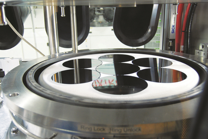
Plessey would like to ramp up UK production, but according to marketing director, Myles Blake, this is unlikely ‘as investment appetites stand’.
Launching LED production at its Plymouth facility in 2010, the company unveiled industry’s first commercially available GaN on 6-inch silicon LED in 2013. Single chip, high-power packaged LEDs and horticultural lighting units followed in 2016.
Now, with new market growth in mind, Plessey has revealed its intention to deliver the industry’s first monolithic microLED displays by 2018. The company’s microLED arrays comprise highly efficient emitters that are as small as a micron and provide some 100,000 nits at 1 W, television-equivalent brightness at only 5 mW. Crucially, using these arrays can overcome the tortuous fabrication issues that plague the lion’s share of microLED displays.
Today’s microLED displays are assembled on a CMOS backplane, one sub-pixel at a time. A 4K television has some 25 million sub-pixels, going some way to explain why most microLED displays have been limited to smartwatches and smartphones.
But as Plessey marketing director, Myles Blake, points out, an array of Plessey GaN-on-silicon microLEDs can be mass transferred onto the CMOS backplane, dispensing with the pick and place minefield and delivering a cheaper, higher yielding manufacture process.
“Display size is purely limited by the size of the silicon, and we are producing our own backplanes that are scalable to any size we like,” highlights Blake. “This allows us to perform rapid custom development, and we can develop a custom backplane in just weeks.”

As Apple, Sony, Foxconn and more embrace microLEDs for spectacularly high resolution, high brightness, low-power displays, industry analysts predict the market will explode.
“Also, due to the capability of the [pick and place] handlers, the size of today’s [emitters] is limited to around 50 microns pixel pitch... but we’ve proven pixel production to one micron, and theoretically we can go down to sub-micron pixel sizes,” he adds.
Blake won’t yet reveal display yield figures, but has announced Plessey’s intention to license its GaN-on-silicon technology to microLED manufacturers. The company is also working with UK-based optical thin film coating supplier, Artemis Optical, to develop very high brightness, low-power head-up displays that are said to be smaller and cheaper than today’s devices.
“We really need to get ourselves out into the microLED market place and build up partnerships throughout the supply chain as quickly as possible,” he says.
Indeed, it’s no secret that the complex and lengthy microLED display supply chain is rather fragmented as bringing together LED production, display manufacturing and assembly isn’t easy. Still as Blake points out: “We are already talking with a large number of display manufacturers and it is never too early to do this. The manufacturing chain is now coming together.”
So what next for Plessey? Right now fabrication takes place on 6-inch wafers and looks set to remain on this wafer size for the foreseeable future.
“We have proven the capability of GaN-on-silicon on 8-inch wafers with our existing MOCVD reactor stacks but we don’t yet have the full equipment set beyond epitaxy to run this wafer size,” says Blake. “And we have yet to start on twelve inch production.”
Plessey also hit the headlines earlier this year with its plans to move towards an intellectual property licensing model rather than ramping UK production. At the time, Plessey chief executive, Michael LeGoff, cited a lack of investment funds, and according to Blake, the company would ‘love to scale production’ but adds that ‘as investment appetites stand, this almost definitely won’t happen in the UK’.
According to Blake, the Plymouth facility currently has two reactors, with associated processing equipment, and could eventually house 14 reactors. Given each reactor can churn out some two million 1mm2 die every week, the potential increase in output rates is significant.
“We will use and also expand this manufacturing capability within the bounds of the current facility,” says Blake. “This will be for research and development, and will include a level of manufacturing... but this is small compared to the [multi-billion dollar] microLED market predictions.” Clearly the marketing director has high hopes for microLEDs. As he asserts: “I believe that augmented reality and virtual reality will go bonkers during the next few years, with microLEDs providing the foundation to supply the anticipated spike in demand.”
GaN template manufacturer, Seren Photonics, is to scaleup processes for microLED displays. Rebecca Pool reports.
Earlier this year, UK-based manufacturer of GaN templates, Seren Photonics, revealed that it had secured £500,000 to scale-up MOCVD growth processes and drive green LED epitaxy on semi-polar GaN development forward.
The cash forms the first tranche of a £1 million funding round and follows several years of 2- and 4-inch semi-polar and non-polar template development targeting wavelength-stable, efficient green LEDs with high light output and reduced droop.
But importantly, it comes at a time when Apple, Sony and many more along the supply chain are eyeballing technologies that can deliver the spectacularly high resolution, high brightness, low power micro-LED screens that the display industry craves.
As Seren Photonics Chief Development Officer, Bedwyr Humphreys, puts it: “Our technology makes longer-wavelength [green, yellow and orange] InGaN/GaN based LEDs more wavelength-stable over a wide range of operating conditions and delivers the potential for improved efficiency through superior electron-hole recombination rates.”
Seren has already demonstrated that the template process can run in a pilot-scale environment and is now honing yields and process control.
“Our aim is to set up our own manufacturing facility at the emerging Compound Semiconductor Cluster in South Wales in around 18 months, whilst continuing to work with our existing partners,” adds Humphreys. “By this time, we want to be able to say: ‘Yes, we have the confidence that the product is doing what we expect it to and, yes, we have significant commercial traction to create a facility and make it a success’.”
Road to green success
Seren Photonics first emerged in 2009 to fabricate high efficiency InGaN/GaN nano-rod LEDs, pioneered at the University of Sheffield, UK. But within a few years, the company had switched focus and was using its growth-on-nanorod and AlN buffer layer approach to produce low-defect-density GaN templates for low-droop blue LEDs and high efficiency green LEDs.
Recent collaboration with Australia-based BluGlass sees Seren working to transfer its semi-polar GaN template process onto the semiconductor manufacturing developer’s MOCVD platform. Later this year, Seren plans to demonstrate the process on 4-inch wafers.
“Our research and development customers are happy to be playing on two inch wafers but LED customers and tech giants need a minimum of four inch wafers,” says Humphreys. “Six inch wafers aren’t a problem either and we will move onto these when they are required.”
According to Humphreys, tier one companies are interested in semi-polar templates to fabricate blue LED devices with reduced droop. Meanwhile, Asia-based tier two companies are drawn to samples of green LED epiwafers.
“Tier one companies tend to have a long-term mindset and are happy to take the template and develop the rest themselves,” points out Humphreys. “But tier twos, particularly those in Asia, simply want a device wafer that they can run through their fab, optimize the process and commercialise the LED.”
Given this, Seren is developing green structures on its semi-polar templates. “Overnight we saw immediate interest for ‘plug and play’ sample structures, when we started talking about green epi wafers,” says Humphreys. “So now we have evolved one step down the supply chain from templates to device epi-structures, although its unlikely that we’ll go any further than that.”
But while demand for semi-polar templates and epi-structures is clearly growing, what about Seren’s non-polar technology? Indeed, from word go, the company has been working on nonpolar GaN on r-plane sapphire as well as semi-polar GaN on m-plane sapphire.
Humphreys reckons customers from the LED industry have historically favoured the semi-polar template as epitaxy structures can be more easily grown on this material. But change is afoot.
“We’re now getting more enquiries for non-polar a-plane GaN for HEMT applications, such as sensors and electronics,” he says. “Non-polar GaN development is on our roadmap but we are focusing on semi-polar templates for optoelectronics right now.”
And without a doubt, optoelectronics opportunities are set to soar. France-based industry analyst, Yole Développement, forecasts more than 300 million microLED displays will be shipped by 2025, dwarfing today’s relatively negligible sales. Meanwhile, Research and Markets, Republic of Ireland, puts annual growth at 53.2 percent, with the global market reaching $19.89 billion by 2025.
Seren Photonics is hardly alone in its wish to grab market share. UK-based Plessey, for one, has revealed its intention to deliver the industry’s first monolithic microLED displays by 2018, while the likes of Aledia, France, and Glo, Sweden, are delivering 3D nanowires for microLED displays. Indeed, Aledia recently won €30 million to drive commercialisation of its 3D nanowire-on-silicon technology forward.
Humphreys describes these monolithic approaches as ‘elegant’ but asserts fabricating micron- to nano-sized red, green and blue LEDs on one chip isn’t easy and better suits smaller screen sizes, such as wearable displays. In contrast, he believes larger displays, including tablets, will benefit from having individual red, green and blue LEDs in the relatively big pixel spaces, making Seren’s technologies for efficient and wavelength-stable green LEDs a real draw.
“Today’s green LEDs have a wall-plug efficiency of less than 20 percent, so in some applications you have to have two green LEDs for every red and blue, raising power consumption,” he says. “Also, c-plane green LEDs have significant wavelength shift at different current densities, something that can cause problems in display applications.”
Given this, Humphreys is confident Seren’s approach provides the answer. “The ability to have LEDs that are wavelength-stable across a range of current densities and operating powers is so very important for these display applications,” he says, “So our focus is about getting green LED wafers out there right now; we’re quickly putting the pieces together and are targeting initial products within six months.”
What does Cree’s acquisition of Infineon’s RF Power arm mean for industry? Rebecca Pool talks to Wolfspeed Vice President, Jim Milligan, to find out more.
In March this year, Cree bought Infineon’s RF power business for €345 million. Shares of the lighting manufacturer shifted 9 percent upwards following the buyout news, and the move will help the company to bolster Wolfspeed’s business position.
The acquisition also comes one year after Infineon’s $850 million deal to buy Wolfspeed fell apart following US regulatory disapproval. At the time, the proposed acquisition fitted in with chief executive, Reinhard Ploss’ desire to grow Infineon’s SiC offering and expand into electric vehicle and 5G telecoms market segments. Then Wolfspeed chief executive, Frank Plastina, also asserted that Infineon would extend his company’s market reach and accelerate SiC and GaN technology commercialisation.
This time around, roles are reversed. But as Jim Milligan, Vice President of RF and Microwave Products at Wolfspeed puts it: “We see this as an opportunity to strengthen the position Wolfspeed has in the RF GaN market, for the same reasons as a year ago.”
This time, the transaction covers Infineon’s Morgan Hill, California, facility, including packaging and test operations for silicon LDMOS and GaN-on-SiC, a plastic packaging services line in Melaka, Malaysia, as well as all-important contacts with wireless infrastructure equipment manufacturers.
At the same time, Wolfspeed will scoop up some 260 employees – including more than 70 RF and GaN engineers – from the Morgan Hill facility as well as Chandler, Arizona, and Finland, Sweden, China and South Korea.
Company figures already indicate that the Infineon RF power business will raise Wolfspeed’s annual revenues by around $115 million in the first twelve months, post acquisition. And in addition to now being able to provide both bare die and packaged devices, Wolfspeed is vertically integrated from SiC wafers to devices, an advantage that the company describes as ‘unique positioning’.
“Infineon’s RF power business is an established leader in silicon LDMOS technology and the acquisition also brings access to more customers, additional markets, high volume packaging and test expertise,” highlights Milligan. “All of this really strengthens our position going forward particularly in existing 4G and emerging 5G markets.”
Indeed, the greater bandwidth and reduced latency that 5G telecoms will deliver, demands more spectrum in ever-higher frequency ranges. And as industry moves from traditional cellular bands, 1.8 GHz to 2.7 GHz, towards 3.5 GHz to 6 GHz bands, Wolfspeed intends to be ready.
“We’ve been playing on the 4G telecoms market with Ga-Non-SiC for a number of years and as we see 5G emerging in higher frequencies, we will really be able to access those opportunities,” says Milligan.
What now?
Going forward and as part of the deal, Infineon will support the transaction with a long-term supply of 8-inch LDMOS wafers and related components from its Regensburg fab, Germany. The company will also supply advanced packaging and test services from its Melaka and Morgan Hill facilities.
“Wolfspeed can now go to customers and offer state-of-the-art LDMOS but also GaN-on-SiC,” points out Milligan. “We are now in the position to provide the optimum technology depending on what the specific needs are.”
The company’s new employees are sprinkled across ex-Infineon operations, worldwide. And as Milligan points out, gaining some 70 RF and GaN engineers is a massive bonus.
“Infineon has a large entrenched base with its RF engineers that provides specific capabilities, particularly in telecoms wireless infrastructure,” he says. “This gives a lot of additional ability o go ahead and address these market very aggressively. The requirements associated with existing 4G infrastructure and the migration to 5G infrastructure is so specialised but [these new employees] bring very good device and systems level knowledge.”
So right now, Wolfspeed plans to double its entire capacity this year, and then, quadruple business by 2022. Indeed, postacquisition announcement, Cree chief executive, Gregg Lowe, told investors he has identified Wolfspeed as a primary growth engine for Cree, given the ‘multi-decade growth opportunity offered with the adoption of SiC and GaN technology in electric vehicles, solar energy, industrial, military aerospace and telecommunications’.
And Milligan can’t wait. “We have these markets as well as land mobile radio, commercial test equipment applications, homeland defense and radar markets,” he says. “We’re really excited about this acquisition and the growth it will provide going forward.”
Intengent, GCS and VLC Photonics have joined forces to deliver an InP PIC platform for wafer fabrication. Rebecca Pool finds out more.
Earlier this year, Canada-based III-V photonics consultancy, Intengent, joined forces with US compound semiconductor wafer fabrication foundry, Global Communication Semiconductors, and photonics IC design house, VLC Photonics, from Spain, to take InP photonic IC development to commercial production.
Together the partners will offer fabless development for the production of customised InP PICs, and Intengent chief executive, Valery Tolstikhin, is certain that the new team has what it takes to deliver a generic InP PIC platform for industrial-grade wafer fabrication.
As he points out, GCS is one of the world’s biggest III-V commercial foundries, churning out InP, as well as GaAs and GaN wafers, for RF electronics and optoelectronics markets in large volumes. Meanwhile, Tolstikhin himself, has pioneered a regrowth-free photonic integration platform – Taper
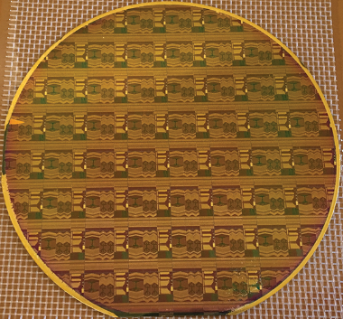
4-inch InP wafer of customised PICs. [GCS-Intengent-VLC Consortium]
Assisted Vertical Integration – based on the GCS’s well established optoelectronics process, for designing and developing InP PICs.
Factor in the VLC Photonics’ design library and process design kit expertise, which is already applied to other commercial PIC platforms and can slash PIC design effort and risk, and Tolstikhin’s confidence becomes understandable.
“Typically, people in the industry have an idea of the application they want to serve but often don’t know what device they want,” highlights Tolstikhin. “So we can conceptualize the PIC that matches that application and develop it through regular designmanufacturing-verification cycles – that’s what we do as a consortium.”
“Intengent provides the integration platform and underlying epitaxy design, VLC brings a wealth of experience in PIC design and characterisation, and GCS is probably the biggest commercial foundry in the III-V photonics domain,” he adds. “I have seen optics increase from 5 percent of GCS’s overall volume to more than 50 percent; this is a huge change and this [one-stop shop for InP PICs] is something I have wanted to be part of for a long time.”
Early days
In the last two decades, Tolstikhin has launched several PIC-based businesses, pioneering various photonic integration platforms based on different versions of vertical integration.
He first became involved with PICs in 2000, when he joined MetroPhotonics, a spin-off from the National Research Council of Canada, set up to commercialise wavelength-division multiplexing technology for InP. Here, he led PIC design until the company folded in 2005, and during this time developed and patented a robust, regrowth-free active-photonic device integration technique called ‘single-mode vertical integration’.
Having developed a number of InP-based WDM components at MetroPhotonics, he went on to launch OneChip Photonics, with a view to developing cost-efficient InP PICs using his regrowth-free PIC technology.
The OneChip business model was based on fabless manufacturing, which Tolstikhin has always touted as being appropriate for low volume markets. And during his leadership at OneChip, he honed his vertical integration process, pioneering ‘Multi-Guide Vertical Integration’.
Here, by vertically stacking the necessary materials for, say, lasers and detectors, the technology allowed the company to monolithically integrate active, as well as passive, devices onto the same substrate in a single epitaxial growth step.
As the chief executive highlights: “I individually designed every single epitaxial structure for every PIC product developed or tried by OneChip, which was an absolutely crucial step in regrowth-free PIC production.”
OneChip went on to develop PIC-based optical interconnects for 100G datacentre market applications, partnered with GCS and IQE on wafer processing and epitaxial growth, but closed in 2014, by which time Tolstikhin had co-founded ArtIC Photonics, a fabless developer of InP-based PICs for telecoms and datacoms markets.
ArtIC remains today, designing PIC chips for optical component products, but in 2015 Tolstikhin founded Intengent to design and develop InP PICs, this time based on Taper Assisted Vertical Integration (TAVI).

Tolstikhin hopes to see ‘real commercial infrastructure’ for the fabless development of III-V photonics, in place within five years. [Intengent]
Building blocks
The TAVI library comprises many building blocks, from lasers to amplifiers to detectors on the active device side and splitters/combiners, filters, and various elements of waveguide circuitry, on the passive device side. What is common to all of them is a lateral taper assisted adiabatic transition between vertically stacked and functionally different guiding layers.
Perhaps, the most generic building block, which showcases the TAVI platform from this prospective, is the spot-size converter that permits the transition of guided light from a PIC waveguide to an optical fibre. This is defined by building lateral tapers in a specially designed multilayer epitaxial structure. Indeed, as Tolstikhin points out: “Intengent has now been working with a commercial foundry on the epitaxy growth of specialised wafer designs that comprise up to 90 layers.”
“It is so important to allow the optical signal to move from one vertical layer to another.... and lateral tapering allows you to vertically connect all of your waveguides,” he adds. “This method is very flexible, it is a big deal and we are seeing big gains in reliability.”
Right now, Intengent is predominantly working on 4-inch wafer sizes with GCS, but intends to transition to 6-inch wafers as soon as possible.
“I would love to work with six inch, even eight inch wafer sizes but these are not readily available right now,” says Tolstikhin. “In terms of cost, size of wafers really does matter here as the number of devices you can harvest is so different from wafer to wafer; this is not like laser development, these really are big chips.”
“I cannot name the date, but six-inch wafer fabrication is coming,” he adds.
Crucially, so is demand. According to Tolstikhin, he is thinking of expanding the company to cope with growing demand for InP-based PICs from various segments of the market, from tele- and Datacom to microwave photonics and quantum inscription.
And at the moment, the chief executive is also seeing interest from silicon photonics businesses demanding III-V integration. “[Designs] now need sophisticated light sources that cannot be provided by off-the-shelf by bulk assembly,” he says. “This is one avenue that wasn’t really evident a few years ago.”
With demand rising, Tolstikhin is now looking forward to seeing what he describes as ‘real commercial infrastructure’ for the fabless development of III-V photonics. He hopes such infrastructure will be in place within the next five years, and importantly, he expects this to be able to provide a full level of customisation, within a reasonable budget.
“Following the development of silicon photonics, many in our industry now understand the need for fabless development and the pointlessness of building an entire infrastructure for just one device,” he asserts. “We are trying to capitalise on this and provide the services that those people want.”
Etching deep, lateral gratings in GaN lasers equips these sources with the credentials to target atomic clocks by Nick Bowden and Thomas Slight from CST Global
What will be the legacy of the Blu-ray player? With the rise Netflix and other video-streaming services, sales of this player could rapidly decline. But the Bluray will still be cherished, in this industry at least, as the product that drove the commercialisation of the GaN-based laser.
The good news is that a second killer application is now emerging for this class of laser: illumination. GaN lasers are already being used in the headlights of high-end cars, and they are a very promising source for all forms of colour projector.
Other markets are also on the horizon. They demand GaN lasers with greater spectral purity and wavelength selectivity, characteristics that may be introduced by replacing the Fabry-Pérot cavity with a distributed feedback design. Making the switch allows the lasers to win deployment in plastic optical fibre networks and to provide communication through water, and last but by no means least, to serve in atomic clocks, where their blue emission is used to cool atoms.
At present, there are two common options for the optical source that is used in atomic clocks: bulky, solid-state lasers, which use frequency doubling to produce appropriate wavelengths; and blue laser diodes with external cavities, a combination that requires complex, vibration-sensitive mechanical assemblies. Replacing either of these sources with a GaN-based laser that features distributed feedback would deliver multiple benefits. It could simplify the design of the clock, slash its size, make it more robust, and ultimately underpin its transition from the lab to mainstream, commercial applications.
To try and turn this dream into a reality, our team at CST, the University of Glasgow, TopGaN Lasers and Aston University has been developing GaN lasers with the required attributes through a project known as CoolBlue. This effort, which is has the official title, Quantum Cooling using Mode Controlled Blue Lasers, has revealed that it is possible to produce a commercially viable, single wavelength, GaN laser diode for atomic-cooled, quantum sensors.
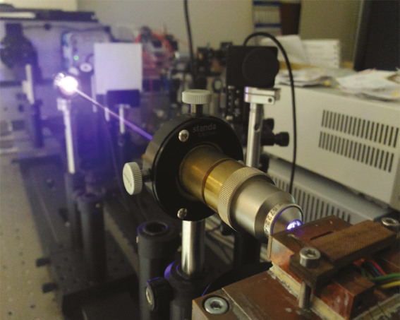
Figure 1. A distributed feedback laser under test.
Credit: S. Stanczyk, TopGaN Ltd.
While the market for this device may never be as big as that for the Blu-Ray player, it can still be significant. According to a 2015 report entitled A roadmap for quantum technologies in the UK (co-authored by Innovate UK, a leading UK Government research funding agency, and the Engineering and Physical Sciences Research Council) the global market for quantum technology is worth about $1 billion. If a third of this is quantum sensing, 10 percent of that is associated with sensing hardware, and one-tenth of that is the laser source, the market for this class of GaN laser diode is £3 million. Project a conservative annual growth of 10 percent, and that is a market of £5.3 million in five years.
Tapping into this market will require volume production of laser diodes that combine many of their well-known attributes – such as a small size and a robust packaging – with a high degree of spectral purity, ideally realised with a relatively simple approach. We are able to do this with our novel form of grating.
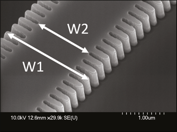
Figure 2. A scanning electron microscopy image of the ‘as etched’ third-order grating, with waveguide widths W1 and W2 of 1.5 μm and 2.5 μm, respectively.
Grating design
Our approach differs from the two conventional ones that have been adopted for the production of distributed feedback laser diodes. One option is buried gratings, which are hampered by complex overgrowth steps that risk epi-defects. With the common alternative – surface gratings etched directly into the ridge top – the danger is a reduction of p-type contact quality, due to damage caused by reactive ion etching. Another impediment associated with surface gratings is a significant optical loss in the electrically un-pumped grating regions, an issue that may be mitigated with shallow-etched, lateral grating designs.
We avoid all of these pitfalls by pioneering deeply etched, lateral gratings. One of the merits of this approach is its reduced number of steps: most of the structure, including the waveguide and the grating, is formed in a single step. Additional advantages are a higher yield and a larger grating coupling coefficient, strengths that we particularly value for producing sources for atomic-cooled, quantum sensing systems, such as atomic clocks.
Fabrication of our lasers begins by taking commercially-available, MOCVD-grown GaN lasergrade wafer material that contains an active region with InGaN quantum wells with GaN barriers, and using an electron beam lithography tool at the University of Glasgow to define grating and ridge patterns. Reactive-ion etching transfers the pattern into a 100 nm-thick, hard mask before inductively coupled plasma etching forms the grating and the ridge. The resultant structures have a nearly vertical and smooth etch profile, to ensure optimal grating performance.
Completion of our devices involves the addition of an electrical contact to the cap layer, before the reverse of the wafer is mechanically-thinned and polished, before a conductive metal layer deposited on it. Finally, the devices are cleaved to different cavity lengths, with both front and back facets left uncoated.
Fabricating of first-order sidewall gratings is challenging, as it requires high aspect ratios and feature sizes as small as around 40 nm. So we use third-order gratings, which have minimum feature size of around 120 nm.
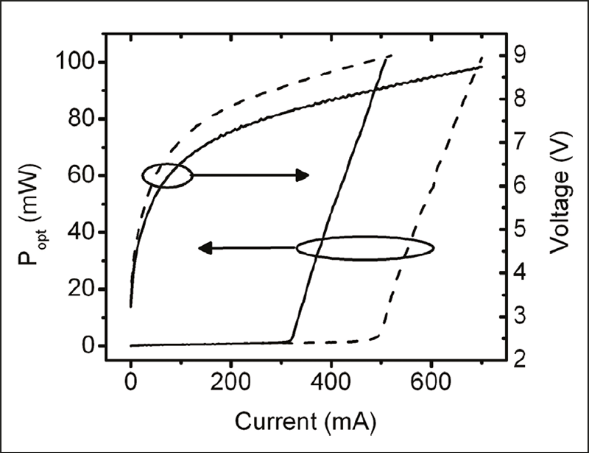
Figure 3. Optical power and voltage as a function of pulsed drive current for distributed feedback device (solid line) and the Fabry-Pérot device (dashed line).
We have undertaken simple modelling to improve our grating design, and gain greater insight into the influence of grating dimensions on device performance. Using the beam propagation method, we have calculated the effective modal index. Then, using this value we have determined that for lateral grating waveguide widths of 1.5 μm and 2.5 μm and an etch depth of 0.5 μm, there is a refractive index difference within the laser of 0.0015. Using this value, and turning to couple mode theory, we can estimate a value for the coupling coefficient of 22 cm-1. To ensure a single mode yield, the product of the coupling coefficient, k, and cavity length should be around 1.5, implying that the optimal cavity length is around 700 μm.
To evaluate the performance of our devices, we have undertaken light-current-voltage and spectral measurements on distributed feedback lasers with a third-order grating that features lateral grating dimensions of 1.5 μm and 2.5 μm, a cavity length of 1000 μm and an etch depth of 520 nm. So that we can benchmark the performance of these devices, we have also fabricated Fabry-Pérot lasers with similar dimensions from the same wafer.
Pulsed drive measurements at 20 °C reveal that the slope efficiencies of both types of laser are similar. However, the distributed feedback laser has a lower threshold current, suggesting that the feedback from the grating is stronger than that from the cleaved facets. Both classes of laser have relatively high threshold currents, which is thought to be primarily due to sub-optimal epi material.
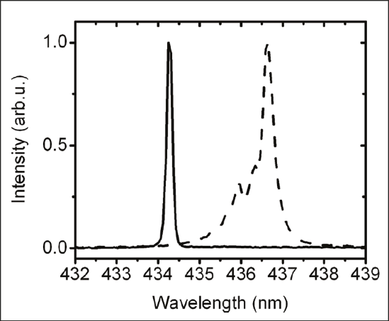
Figure 4. Single wavelength emission for distributed feedback device (solid line) and, for comparison, multimode spectra of the Fabry-Pérot device (dashed line).
Atomic aspirations
As expected, the emission from the distributed feedback laser is much narrower than that produced by the cousin with the Fabry-Pérot cavity. While the latter exhibits multi-mode emission, the distributed feedback laser produces a single wavelength emission spectrum (see Figure 4). At a drive current of 390 mA, which is 20 percent above threshold, this laser produces an output of 40 mW and has a spectral purity, judged in terms of the side-mode suppression ratio, of 22 dB. These values are sufficient for laser cooling within atomic clocks. However, meeting all the requirements for that application will require more work, including the realisation of continuous wave operation, and the shifting of the emission to 422 nm to target the Sr+ ion.
While reaching an emission wavelength of around 422 nm will get in the right ballpark for the Sr+ ion, temperature tuning is needed to hit the cooling line. To assess the capability for this, we have measured the performance of another distributed feedback laser, which has an emission wavelength of around 437 nm.
By varying the heat-sink temperature between 20 °C and 30 °C, we can tune the emission wavelength during pulsed operation. This device has a tuning coefficient of 0.013 nmK-1, which compares well with published values for lasers of this type.
Thanks to the successes that we have had, we have won funding for a follow-up project, CoolBlue2. It started in April 2018 and runs for a year. All the partners in the first project are retained, and are joined by the National Physical Laboratory (NPL) and Helia Photonics. The role of NPL includes performing laser cooling system tests to demonstrate the efficacy of the technology, while Helia is offering expertise in laser facet coating, enabling improvements in laser performance.
We hope that the GaN technology that we develop in CoolBlue 2 will form the critical elements in many quantum applications. This effort should result in a stringent set of performance requirements for wavelength, stability, output power and linewidth, and will offer a clear understanding of how lasers can be deployed in many different applications.
Looking even further ahead, after CoolBlue 2 has finished, those of us at CST will continue to invest in product development, assuming sufficient visibility of market opportunity and maturity of the supply chain. This investment is likely to be at the chip or packaged device level, although clearly opportunities may exist for subsystem-based products.
This work was supported by the Innovate UK project Coolblue (project number 132543) and by The National Centre for Research and Development within the Eurostars 2 Programme (E10509/29/NCBR/2017)
Further reading
T. J. Slight et al. IEEE Photon. Technol. Lett. 28 2886 (2016)
Employing the mass production techniques of the optoelectronic industry will increase the bang-per-puck of CPV by Richard Stevenson
It would be easy to think that the CPV industry has completely disappeared. Deployment of this technology has fallen through the roof, with many big names having filed for bankruptcy over the last few years.
However, there is still activity – and with that comes hope. Early last year STACE – Saint-Augustin Canada Electric Inc., a supplier of large electrical equipment in the power generation industry – acquired Soitec’s CPV technology; and in Europe, a collaboration between several companies is currently developing a lower-cost, highly efficient CPV system that borrows high-volume manufacturing techniques from the optoelectronics industry.
The latter project was detailed at Advances in Concentrator Photovoltaics for Space and Terrestrial Applications, held at Cardiff University on 8 March. Spokesman for the project, entitled A low Cost, High Efficiency, Optoelectronic HCPV Module for 1000 Sun Operation, was Andy Johnson, IQE’s Solar Business Unit Leader and CPV Technology Director.
According to Johnson, the focus of the €1.24 million project is to improve the performance of the FullSun CPV modules. The starting point is a design that has a concentration of 625 suns, and produces an efficiency of 30 percent by harnessing concentrated sunlight with cells that have a 36 percent efficiency. The targets are to increase efficiency to 1000 suns, and to realise a 37 percent module efficiency using triple-junction cells with a higher efficiency than before.
Three different triple-junction cells are being evaluated in the project: a generic, lattice-matched design from IQE that has an efficiency of 39 percent or more at 1000 suns; an Azur Space 3C44 cell, which has an inverted metamorphic architecture with an efficiency in excess of 42 percent at 1000 suns; and a latticematched device made by Solar Junction, which features a dilute nitride for the low-energy junction. “Solar Junction’s materials was grown by MBE,” said Johnson.
The philosophy behind the module, made by FullSun, is to adopt best practice from the optoelectronics industry, including the use of surface mount technology. This approach, which drives down capital costs, involves the use of cells that are just 1.3 mm square. These cells, which are covered by a silicone lens and packaged on lead frames, are sparsely arranged on an aluminium back plane. “There is no need for additional heat sinking,” explained Johnson.
Benefits of this design of module include reduced maintenance and purchase costs. What’s more, the units have a low mass – they are less than 4 kg – and a thickness of just 48 mm, making them easier to transport; and installation is straightforward, trimming labour costs.
Johnson explained that a team at Fruanhofer ISE is behind the changes to the optical design of the module that is propelling the concentration from 625 suns to 1000 suns. Given a target area of 1 mm by 1 mm, the team retained the secondary optical element – that is, the silicone lens on top of the cell – and just adjusted the primary optical element, the Fresnel lens. Its focal length could be changed.
Another partner in the project is the III-V Semiconductors Group at the Solar Energy Institute of the Technical University of Madrid (IES-UPM). This team have worked on optimising the grid on the 1.3 mm by 1.3 mm cells, by evaluating the impact of varying grid line width and the number of fingers. They considered using between 12 and 25 fingers, and found a sweet spot of 14 to 18. The team’s next step is to compare the performance of different grid structures.
These researchers only have a few more months to work on this. Assembly of the 1000 sun modules is slated for the third quarter of this year, and testing is scheduled to follow in quarter four.
These field tests will take place at the University of Cypress, an ideal location for putting any photovoltaic system through its paces. It is hoped that this design, which will be mounted on a two-axis tracker, can get close to a cost of €0.35/W to €0.45/W.
Ensuring reliability
This metric is widely used. However, its validity was questioned in a talk given by Carlos Algora, head of the group at IES-UPM. He championed the use of the levelised cost of energy, which is equal to the total lifecycle cost, divided by the total energy generated over the lifetime of the system. According to Algora, this is a superior figure of merit, because as well as including the initial purchase price of the system, it accounts for maintenance and operational costs and the lifetime of the system.
Algora went on to point out the importance of the reliability of the cells – this impacts degradation, operation, maintenance and system lifetime. He stressed that reliability is different to qualification. According to him, the purpose of qualification is to try and give confidence to customers, and to avoid infant mortality, while any assessment of reliability ideally involves field tests. However, as deployments of CPV systems are recent, reliability has to be gauged with accelerated lifetime tests.
“The purpose [of the reliability tests] is to find out how, when and why failure will occur,” explained Algora, adding that the right approach is to stress one parameter while leaving all others unchanged.
Tests were undertaken on 45 commercial, latticematched, triple-junction cells with dimensions of 7 mm by 7 mm. Standard operating conditions for these cells are a concentration of 820 suns, and a device temperature of 80 °C. To accelerate degradation, cells were stressed at 119 °C, 126 °C and 164 °C, while driven at a forward current of 3.2 A to emulate the intensity of illumination of sunlight on the device. Measurements of current-voltage characteristics offered an insight into degradation.
Using an Arrhenius-Weibul model, Algora and coworkers determined that the probability for cell failure after 25 years is only around 0.1 percent, and that the warranty time for a 5 percent failure rate is more than 110 years, assuming 5 hours of operation per day.
At first glance, that looks like a great result. However, Algora warned against getting too excited, because cells don’t work at a constant temperature. He argued that the key question is this: “How long will they work in real conditions?”

Advances in Concentrator Photovoltaics for Space and Terrestrial Applications, was held at Cardiff University on 8 March.
To try answer this, he and his co-workers have carried out calculations for a cell operating in a CPV system featuring a Fresnel lens. They determined operating temperatures for different ambient temperatures and wind speeds, for cells in CPV systems situated in Madrid, Denver and Tuscon.
For Madrid, the mean temperature is an encouraging 67 °C, while the figure for the mode is 78 °C. However, there are times when the cell exceeds 100 °C.
“When the temperature is greater than 100 °C, this has a tremendous impact on solar cell performance,” revealed Algora, who explained that this shortens the warranty time from over 100 years to just 35 years.
In Tuscan, the cells could get even hotter, spending some time above 110 °C. This slashes the warranty time for the system to 15 years. Meanwhile, in Denver, where it is cooler, the warranty would be 60 years.
Obviously, it is critical to prevent the cells from running at high temperatures. One option is to increase the thickness of the back plane to enhance heat dissipation, but this adds not only to the weight, but also the bill-of-materials and the shipping costs. Reducing the concentration would also lead to lower chip temperatures, but at the expense of less generated power.
Better still, argued Algora, is to use smaller cells, as they are better at dissipating the heat. It’s a point that Johnson and his partners would have delighted in hearing, as this is the route they have adopted.
During Algora’s talk, delegates were reminded of the insights that can be made by modelling the performance of the CPV module. Up until very recently, the barrier to this had been the need to write code to simulate a CPV system – but that’s no longer the case, thanks to the release into the public domain over the last few months of a model developed at Imperial College London.
Diego Alosno-Álvarez highlighted the capabilities of this software. The code, which has been developed by the team at Imperial over many years, has been released as an open source this year. The current form, Solcore 5, builds on its predecessors by including tunnel-junctions in device design.
Features of this open source, which is considered to be both a teaching and a research tool, include: a database for the properties of III-V, silicon and germanium; and an option to select either a laser, an LED, a form of Blackbody radiation or a standard solar spectrum as the illumination source.
A limitation of the current model is that it is not equipped with ray-tracing for micro-textures, such as plasmonic structures. Addressing this could be one of the goals for the future, explained AlosnoÁlvarez, along with improved documentation and benchmarking of the software.
The insights provided by this tool, by the work of Algora, and by the IQE-led team developing a 1000-sun concentrator should improve the competitiveness of CPV. But there is no doubt that this elegant form of photovoltaics still has a long way to go before it can slacken the vice-like grip that silicon has on this market.
The capabilities of the Ferrotec UEFC-6100, which has a capacity of twenty-five 200 mm substrates, are not limited to efficient, uniform growth of metal layers – this tool can also deposit highly uniform oxide coatings by Shihu Deng and Philip Greene from Ferrotec - Temescal Division
The history of semiconductor manufacturing attests to the many advantages that come from moving to larger wafers. These benefits provide both a motivation and a driving force for the development of tools that are capable and efficient at undertaking processes on larger wafers. By succeeding in this endeavour, equipment providers can make their customers happy, by giving them an edge over their peers.
For different technologies, different diameters are adopted by the leading manufacturers. For silicon ICs, 300 mm represents the state-of-the-art. Meanwhile, for many other technologies – including GaN-on-silicon devices, such as microLEDs; SiC; filters, in the form of FBAR and BAW; MEMS on silicon; and thin-film batteries – the goal is to move to efficient processing on 200 mm wafers.
At Ferrotec of Livermore, CA, we are serving the needs of device makers with our latest generation of Ferrotec electron-beam evaporation tools. Our entire UEFC tool series is designed to deliver excellent uniformity and throughput on wafers up to 200 mm in diameter. For 200 mm wafers the UEFC-4900 can process 15 wafers/batch at a 0.9 m source-to-substrate distance, while the UEFC-5700 can process 18 wafers/batch at a distance of 1.07 m. The latest version, the UEFC-6100 further increases the batch size to 25 wafers, and can process at 1.07 m or 1.17 m for tighter design rules. This process equipment can efficiently and consistently deposit metal and oxide films.
This equipment portfolio may be better known for the creation of tools that provide efficient deposition of metals on 200 mm wafers of metals, prior to liftoff processing. However, the process equipment can also be used for the growth of optical oxide coatings.
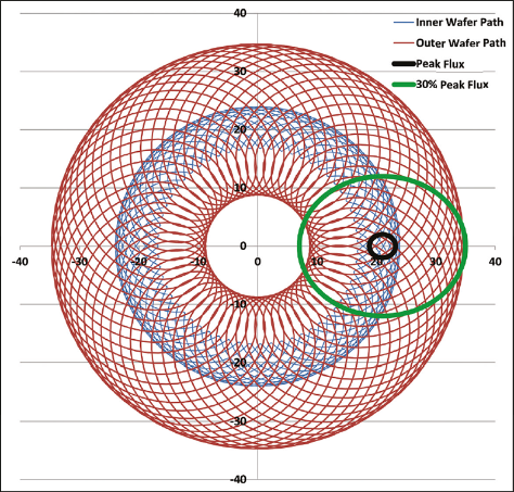
Figure 1. The path that different regions within the wafer take through the chamber leads to a high degree of thickness and incident ion impingement uniformity.
The recently released UEFC-6100 sports these credentials, delivering excellent performance and flexibility by balancing a range of constraints, including thickness uniformity, material utilization, batch size (wafer count), and the basic metric of throughput per squarefoot of cleanroom floor space. Key features of the tool are: the conic product chamber; its capability to use two, three or four high-vacuum pumps; a dual-axis high uniformity lift-off apparatus (HULA) wafer motion, driven by non-contact magnetic gearing; a throw distance that is compatible with design rules for photo-resist structures (the incident angle must be less than 5°); and a ‘load-lock’ separation between the substrates and the electron-beam source.
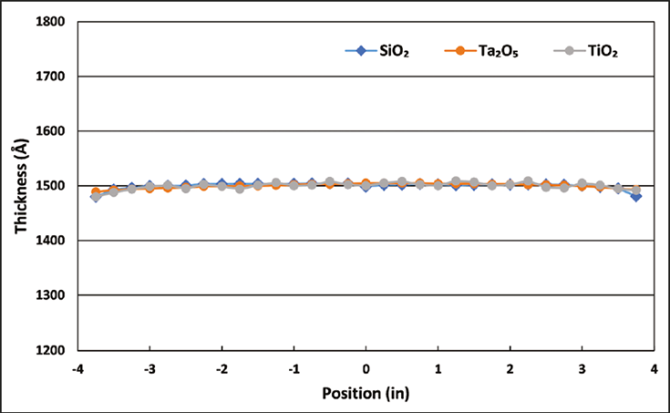
Figure 2. Films of SiO2, Ta2O5 and TiO2, grown on 200 mm substrates by ion-assisted deposition, have a non-uniformity range of around 1 percent.
To highlight the capability of our UEFC-6100, in the remainder of this article we will present the results associated with the deposition of thin films with our tool. Results were obtained using a source to substrate distance of 1.17 m.
For this effort, three cryo pumps were installed in four possible high vacuum pump locations, a configuration that enables the entire system to be pumped down to a pressure below 5x10⁻⁷ Torr in just 34 minutes. If the product chamber portion alone needs to reach this pressure, pumping takes just 28 minutes. Obviously, adding a fourth pump trims those times.
We equipped the UEFC-6100 for this work with a 12 kW electron-beam power supply and a STIH-270-3CK (Poptop) electron-beam source, which limits contamination between pockets. To enable the tool to provide ion-assisted deposition, it was also fitted with a Veeco Mark-II+ grid-less end-Hall ion source.
Another feature of the UEFC-6100 is that by drawing on knowledge of the shapes of evaporation vapour clouds, the dual-axis, non-contact magnetic HULA drive maximises the evaporated material collection efficiency on a full cassette of 25, 200 mm wafers. This enables a metal deposition with non-uniformity that is near 1 percent or less across a wide range of conditions.
We are keen to stress that many features that lead to enhanced performance for metal films also lend themselves to the increased performance of oxide coatings. The design of the tool is particularly well suited to the growth of high-quality optical films, including anti-reflection and high-reflection coatings.
A compelling attribute of the UEFC-6100 is that the uniformity across multiple large-diameter substrates has little sensitivity to the multiple deposition conditions. There is very little difference in nonuniformity between materials. Note also that changes in the deposition rate, gas background and even ion source settings have little influence on nonuniformity, implying that the tuning of conditions for optical properties should not involve efforts to adjust thickness distributions via the use of varying shape uniformity masks.
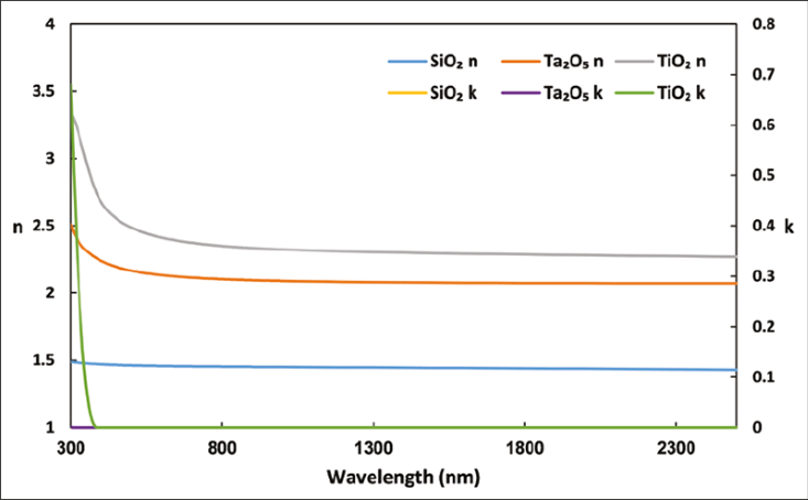
Figure 3. Ellipsometry determines wavelength-dependent values for the refractive-index coefficient and the extinction coefficient.
One of the strengths of our system is its dual-axis substrate motion, which improves uniformity of ion source impingement on the growing films. During film growth, the various locations on the wafer intersect with different intensity regions of the ion source (see Figure 1). The complex path taken by the wafer helps to increase the level of uniformity of the incident ion flux across the full surface.
Optimised optical coatings
To demonstrate the advantages of our tool, we deposited individual layers of SiO2, Ta2O5 and TiO2, as well as optical coatings formed by stacking these oxides. Of great promise is TiO2: it has a very high index of refraction, giving it the potential to improve the performance of many optical designs. For example, in a quarter-wave high-reflectance stack, the tremendous contrast in indices between this oxide and a far lower index material increases the peak reflectance value and the width of the high-reflectance band. However, TiO2 is a challenging material to deposit, for reasons we shall detail in due course.
A non-uniformity range of around 1 percent, as realised in the system for pure metal depositions, can also be maintained with ion-assisted oxide films. This can be seen in measurements of the thickness variations in SiO2, Ta2O5 and TiO2 films that are grown on 200 mm substrates (see Figure 2).
To evaluate the quality of these films, we employ spectroscopic ellipsometry to determine indices of refraction and extinction coefficients. The values obtained reveal that all three materials exhibit very low absorption in the visible and the near-infrared range (see Figure 3).
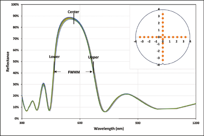
Figure 4. Reflectance values, obtained at 24 positions over a 200 mm glass substrate with an eight-layer stack of SiO2 and Ta2O5.
Spectroscopic ellipsometry can highlight a significant weakness associated with TiO2: its index of refraction is more sensitive to deposition conditions than that of other oxides. The index of refraction is influenced by both the uniformity of the deposition rate and the ion flux incident on the growing film. However, the good news is that with the UEFC-6100, films of TiO2 have very uniform thickness and film properties across the entire 200 mm wafer, thanks to the complex movement of substrates through high and low flux regions. Across the full substrate area, the average index of refraction at 550 nm is 2.44, and the ‘onesigma’ variation is only 0.16 percent.
These results are encouraging, but what is critical is the capability for multi-layer stacks. To investigate this, we began by growing quarter-wave stacks. They are common building blocks for high-reflectivity coatings, such as distributed Bragg reflectors.

Table 1. Variations in reflectance profiles, judged in terms of ‘one-sigma’ values’, highlight the high degree of uniformity possible with the UEFC-6100.
One of the structures that we have grown is an eight-layer, quarter-wave stack of SiO2 and Ta2O5. Measurements at 24 locations highlight the high level of reflectance uniformity across this 200 mm wafer (see Figure 4 and Table 1).
We have also produced a 16-layer, quarter-wave stack of SiO2 and Ta2O5. Its reflectance profile has a very high degree of correlation with that of a model (see Figure 5), with the results showcasing the potential of this stack as a building block for coatings such as a DBR.
In short, our efforts show that although the UEFC-6100 has been initially designed for metal coating uniformity and efficiency, it capabilities have much promise for the production of optical coatings.
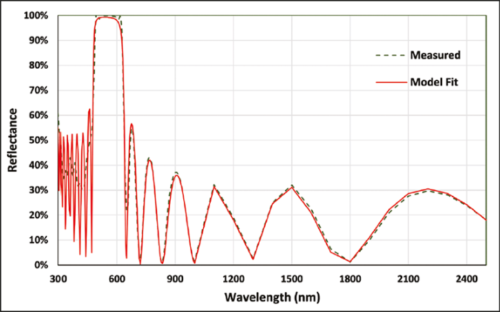
Figure 5. There is a high degree of correlation between the measured values of reflectance for the 16-layer quarter-wave stack of SiO2 and Ta2O5, and the result generated by the model.
LEDs are displacing high-pressure sodium lamps, because they can speed plant growth by optimizing illumination by Alexander Wilm from Osram OPTO Semiconductors
Between 2016 and 2022, it is predicted that the demand for packaged LEDs in horticulture will grow significantly. It is safe to say that the LED industry’s growth has been significant, and shows no sign of stopping.
While some of the reasons that horticulturalists are investing in LED lighting are no different from those that you and I are using when we replace our incandescent and compact fluorescent bulbs – all of us place a premium on high efficiency and a long lifetime – there are additional considerations when it comes to crop growth. The most important of these is obviously the impact of light on crop yield.
Horticulturists have no doubt that LEDs are the ultimate light source on the market today. Implementing LEDs is ushering in a new wave of enhanced growing performance. These improvements exist in practically every area of lighting – from energy costs to adjustability. And it is not just the crop growers who are experiencing the benefits of LED-based horticultural lighting – researchers and greenhouse manufacturers, who deal with luminaires for growth on a massive scale, are privy to the perks.
Trumping high-pressure sodium
For decades, the market leader in horticultural growth has been a form of high-intensity discharge light: the high-pressure sodium lamp. Its great strength is that it produces an impressive output. However, it has three major weaknesses: the light that it emits is distributed across a wide spectral range, so it is not optimized for photosynthesis of plants; it emanates intense heat, so it must be placed well away from crops, so they don’t overheat and dehydrate; and it has a typical lifespan of 8,000 hours. That lifetime doesn’t compare well to that of an LED, which can operate for 50,000 hours, while slashing energy costs by 40 percent compared to the incumbent.
Lighting manufacturers must make sure that their products can operate in high temperatures, such as up to 75 °C. LEDs can fulfil this requirement, and also work in environments with high levels of humidity and moisture, conditions that are often associated with plant growth.
Another reason why horticultural LED sales are mushrooming is that they are able to tap into advances in technology. This is allowing the growers of crops to control light more directly than in the past, leading to higher yields. It is now possible to optimise the lighting for a crop, in terms of colour spectrum, wavelength and the incident power. Practically all aspects of horticulture are now supported by LEDs, as they are able to offer growers optimised emission at 450 nm, 660 nm and even 730 nm – and also provide white lighting. By giving horticulturalists a source of lighting that can tailor the spectral output, these growers can be more precise than ever when it comes to finding the ideal illumination conditions for their crops – they can even use white LEDs, if they need a continuous spectrum. This degree of control could, by itself, have driven the popularity of the LED in the horticultural market, as this is a capability that high-pressure sodium cannot do as effectively.
Experienced horticulturists, and growers on a larger industrial scale, often produce their crops in huge indoor farming facilities. These environments offer many benefits, including the ability to stave off crop-killing animals, protect plants from adverse weather conditions, and tailor the spectra of the light that impinges on the plants to maximise the rate of growth.

Announced at Lightfair in late 2017, the prototype Oslon Square Hyper Red has a wavelength of 660 nm and can control the growth of blossom. This high-power LED features an integrated 2 mm x 2 mm chip and delivers a typical radiant power of 905 mW with radiant efficacy of 60 percent at a current of 700 mA and an operating temperature of 25 °C.
Optimising the source
To optimise yield, growers have to research the optimum lighting conditions for their crops. For first-time growers, this can be a daunting experience, as they will have much to reflect upon, while encountering various units of measurement that can seem alien. However, they must get to grips with them, in order to be equiped with a clearer understanding of specification sheets and of performance calculations, which will aide the purchase of the most appropriate horticultural lighting.
Growers might begin by referring to light specification sheets, which generally use lumens as their form of measurement. But this can be a pitfall for the unwary, because lumens are a measure of the responsivity of the human eye to energy wavelengths – they are not a metric for determining how plants react to different wavelengths of light.
There are several units of measurement for assessing the projection of a light spectrum by an LED that are of interest to horticulturists. They include micromoles per second (μmol/s), a unit that indicates the number of photons emitted from an LED. The micromoles are usually measured in terms of photosynthetic active radiation in the range 400-700 nm. There is also photosynthetic photon flux density, which is the number of micromoles per second that reaches a certain area within any given second.
As growers carry out their research, they will realise the importance that colour has on the growth of crops. A common misconception is that because plants normally grow outside, indoor light should try to mimic natural light. But that’s not the case, and it has been proven that the spectral composition can influence plant growth acutely. In fact, it is this strong dependence on the emission profile that explains why LEDs have come to benefit the horticultural industry so drastically. Note that wattage is also a relevant indicator in growing plants, but it is not the most important factor, because each LED and light source will have differing radiometric lighting efficiency, depending on the product.
Today, many industrial-sized greenhouses are still lit by high-pressure sodium lamps. But, as we have shown, this is legacy technology does not offer the same advantages as LEDs do. The latter will continue to improve and make great inroads into horticultural lighting, where its benefits will increase as growers learn to further exploit its advantages for growing crops faster, and with higher yields.
Atomic layer etching promises to improve the quality of GaN-based HEMTs and eradicate the damage associated with high etching rates by Mike Cooke and Andy Goodyear Oxford Instruments Plasma Technology
All the latest market trends from the Internet of-Things to mobile technology and driverless cars have a common thread: hi tech on the move. This is propelling the industry along a well-trodden path of ever greater functionality, in a smaller and smaller space, while consuming less and less energy. Progress on all these fronts has hinged on the growth of ever thinner films and smaller device features. To do this, there is a need to create and control materials with ever increasing accuracy.
For thin-film deposition, a technology that delivers the goods is atomic layer deposition (ALD). In comparison, conventional plasma etching, which is based on a continuous ‘analogue’ process, fails to offer the same degree of control. But atomic layer etching (ALE) could change all that and propel plasma etching into its ‘digital’ age.
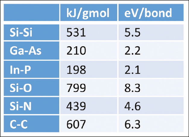
Table 1. Bond strengths of diatomic molecules, from the CRC Handbook of Chemistry and Physics, 1980
The inherent drawback of plasma etching is that it has to accomplish two contradictory tasks: to etch a material quickly, with good selectivity to a mask material; and to leave the exposed surface undamaged. Success is not easy, given that it is hard to imagine anything more damaging to a material than to break its solid atomic bonds, form new volatile compounds and pump these away as gas.
Yet that is precisely what is undertaken to fulfil the first goal: the surface is exposed to chemical radicals and bombarded with energetic positive ions. These act in synergy to allow volatile compounds to be formed. For example, the etching of InP in a methane/hydrogen plasma involves the formation of volatile trimethyl indium and phosphine.
Often, the ion energy used for plasma etching is ten times higher than the bond strengths of solid compounds (see Table 1). This energy is so high that it can render several atomic layers of the surface amorphous. This promotes rapid etching by allowing chemical radicals to penetrate the surface, but a common major drawback is failure to fulfil the second goal, which is to form a pristine surface. A more promising approach is that of ALE. This offers a way to etch with far less damage, using the same synergy of chemical radicals and ion bombardment. However, the key difference is that this time there is a cyclical process of chemical exposure and ion bombardment, using ion bombardment energies much closer to the threshold for breaking bonds (see Figure 1). One of the strengths of ALE is that it offers the possibility of self-limiting reactions, which can remove material with the precision of one atomic layer per cycle.
At Oxford Instruments Plasma Technology of Yatton, UK, we have recently released etch tools that are capable of ALE. Associated with this effort, we have demonstrated that the adsorbed gas is really responsible for the etching, by modifying the cycle so that it omits either the gas step or the ion bombardment step: both are essential for etching to proceed. We have found that the gas that is adsorbed forms a reservoir for plasma etching under ion bombardment, and if the bombardment step energy is low enough, etching stops when the reservoir is exhausted.
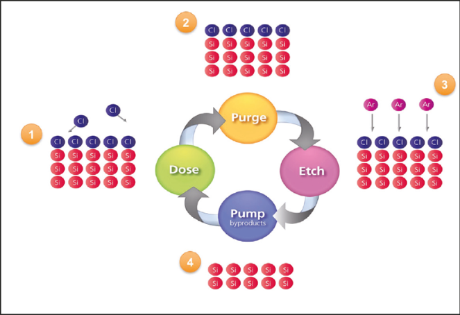
Figure 1. The atomic layer etch cycle. A chemical dose adsorbs on the surface and excess gas is purged away. An etch step under ion bombardment removes the adsorbed radicals together with their chemisorbed partners, ideally stopping once the chemical reactants are exhausted. A pump step may be necessary to clear reaction products before the next chemical dose. Note that this process was proposed more than 20 years ago (see S.D. Athavale et al. J. Vac. Sci. Technol. B 14 3702 (1996)).
Another attractive feature of ALE is that, like atomic layer deposition, if a self-limited reaction takes place, this can produce a plateau where the etch rate per cycle is less sensitive to variations in process variables. We have observed this when etching silicon – there are conditions where the etch rate varies only slowly over a range of RF bias power in the ion bombardment step (see Figure 2).
It would be wrong, however, to view ALE as the mirror image of atomic layer deposition. There are constraints in etching, such as selectivity, so the preferred process is likely to be in the initial steeply varying part of the curve. This places increased emphasis on the precision of delivery at around 10 W RF bias power, which needs to be reproducible to within 0.1 W.
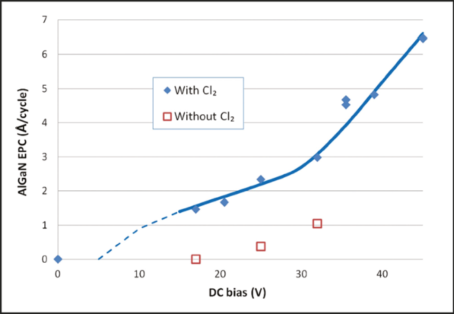
Figure 2. The etch per cycle of amorphous silicon with and without chlorine dosing in an ALE cycle using argon plasma, as a function of the DC bias voltage created by RF power applied to the wafer.
An insight into what is taking place in the ALE cycle is provided by optical emission spectroscopy. This technique can track, throughout the cycle, light emission from chlorine and silicon species in the plasma (see Figure 3).
By analysing the results of this spectroscopic measurement, we have found that the chlorine floor level remains constant throughout the cycle, rather than building up over time. This indicates that the pumping-out step between the dose and etch steps is sufficient.
We have also observed a rapid removal of silicon, followed by a decay in light from silicon species. This points to the end of silicon etching, once the adsorbed chlorine has been used. Note that it is essential that new chemical reactants do not reach the surface during the ion bombardment step. If that were the case, the process taking place would not be ALE, but simply standard plasma etching.
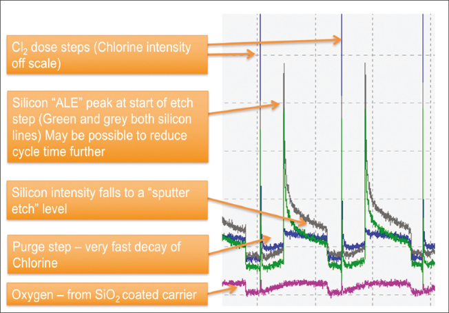
Figure 3. Optical emission spectra of silicon, chlorine and oxygen lines during cycles of atomic layer etching of silicon.
Opportunities for ALE
A key question for the future of ALE is whether this process technology is going to be a curiosity, limited to a few examples, or a new general technique. On the plus side, the list of materials etched by ALE is growing, along with interest in the method, as shown by the rising volume of patent applications in recent years.
One of the opportunities for ALE is in the power electronics industry. For the normally off GaN HEMT, a critical step in the production process is the etching of the gate – the GaN cap layer is removed, before a thin AlGaN layer is etched part way through. To ensure a high-performance device, the material that remains must be as undamaged as possible. As the etch depth is only 10-20 nm, a slow, very reproducible etch rate is needed.
ALE is more than up to this task. Success has been proven by HRL Laboratories – it has demonstrated excellent uniformity of threshold voltage across full wafer size. In addition, using our system, we have demonstrated that it produces a surface roughness below 300 pm in AlGaN, even after 200 etch cycles, so it has capability far beyond what is required. We are currently involved in several projects, such as the ALEGRO project, to demonstrate the capability of the ALE technique to enable normally off operation.
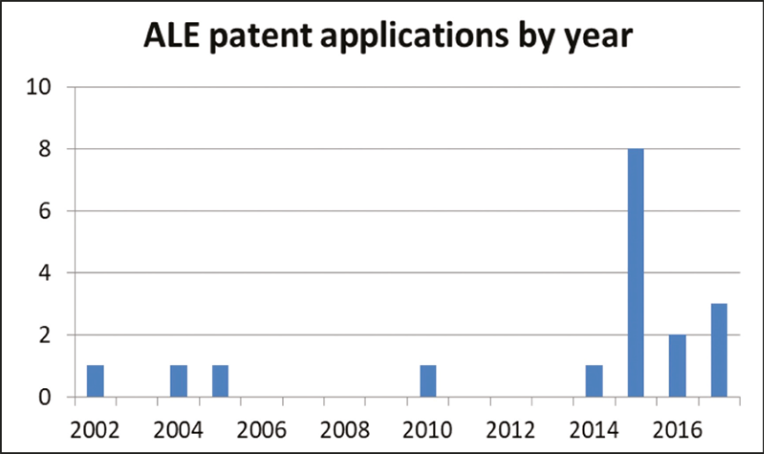
Figure 4. Patent applications citing ‘atomic layer etch’ by year. Date of first filing of patent family.
A related opportunity exists in CMOS manufacturing, because a similar etch is used to remove a gate stack down to a gate dielectric. This opens the gate dielectric at source and drain. A high-quality etch is needed, as any residual damage adds to contact or channel resistance.
Peering in to the future, there could become a time when active devices are formed from one or more layers of atomically thin two-dimensional materials, such as graphene or transition metal dichalcogenides. ALE could have a role to play here. We have used this technique to etch MoS2 with very low damage. The lack of damage is revealed by Raman spectroscopy, which has the absence of a peak at 227 cm-1 that is known to be characteristic of disrupted material (Figure 5). The evolution of a pair of peaks in the Raman spectra also offer evidence that the material, just a few atomic layers thick, was etched during the process.
A hybrid approach
Further opportunities exist as uses for ALE, thanks to its ability to deliver low damage etching. However, as the ALE rate is too slow to process more than a few tens of nanometres economically, it is often best to begin with a traditional high rate etch, before switching to ALE to remove the damaged surface layer. ‘Soft landing’ etches have been used before, but ALE combines etching at the lowest ion bombardment energies with a very high level of precision.
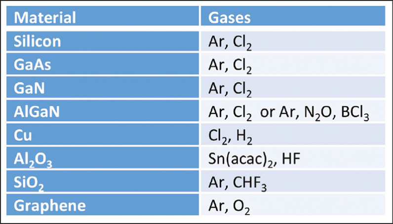
Table 2. Materials etched by ALE.
We have a tool that combines both processes in a single process module. We selected for our starting point the PlasmaPro 100 etch module with 3 kW inductively couple plasma source and a 600 W bias power to the table.
One of the key modifications we made to this tool is to the gas dose hardware. It can now support gas pulses with a duration down to 10 ms, controllable to 1 ms, fed from a low-pressure source. This allows very low doses of gas to be admitted with very fine control on the dose quantity. The mass flow controllers for the pulsed gases reside in an external gas box, as normal.
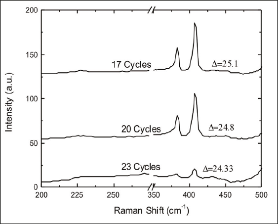
Figure 5. Raman spectra of MoS2 after a number of ALE cycles. The peak separation narrows, indicating removal of layers, and no damage peak builds up at 227 cm-1.
Additional alterations that we made include a low bias control, allowing both full bias power and fine control in a very low bias range. Note that the hardware is not dependent on a specific model of RF generator. In addition, we have enabled the tool to handle fast cycle recipes, with step times controllable to 1 ms, from a minimum step time of 10 ms.
Thanks to all these modifications, our standard plasma etcher has a far wider processing space. It can now operate in a low bias regime, suitable for standard etching; and it can operate in the atomic layer etch process regime, without the need to invest in a dedicated ALE module.
The history of Atomic Layer Etching
The acronym ALE was originally used for atomic layer epitaxy, but this evolved into atomic layer deposition (ALD) as the technique developed. Curiously, atomic layer etching emerged in the same conferences – the International Atomic Layer Epitaxy Symposium, in Helsinki 1990 and Raleigh, USA, 1992 – but the technique was described by other names. In 1992 Y. Aoyagi et al. published a paper at this conference entitled Atomic layer manipulation of III-V compounds (Thin Solid Films 225 120 (1993)), where they named the layer-by-layer subtraction of material MLE, short for molecular layer etching. Others at the same conference called the technique ‘digital etching’ (e.g. J. Yamamoto et al. Thin Solid Films 225 124 (1993)). Athavale and Economou started referring to ‘atomic layer etching’ from 1995 (J.Vac.Sci. Technol A13 996 (1995)), using the acronym ALET to distinguish etching from epitaxy. This acronym, sometimes written ‘ALEt’, has persisted, but is now more commonly abbreviated to ALE.
Further reading
A Goodyear, M Cooke European patent application EP16187143 (3 September 2015)
Wafer-bonding creates a photovoltaic that could set a new benchmark for efficiency, by combining a high-energy GaInN junction with those made from GaInP, GaInAs and germanium by Kazuya Takahashi, Noboru Muramatsu, Motoaki Iwaya, Tetsuya Takeuchi, Satoshi Kamiyama and Isamu Akasaki from Meijo University and Hiroshi Amano from Nagoya University
There is no doubt that the silicon solar cell is a tremendous success. Thanks to improvements in efficiency and a dramatic reduction in price, there are now parts of the world where it is cheaper to build and run a solar farm based on silicon than it is to build a fossil-fuel power station.
However, the silicon solar cell still has it weaknesses. Topping this list is its low efficiency – the best silicon panels on the market operate with an efficiency of up to about 25 percent, and more common is a value in the high teens. Inefficiency is tolerable when land is cheap and there is plenty of space. But that’s not always the case – and there are many situations where a higher premium is placed on efficiency, due to limited space. This situation arises when cells are deployed on a space station, or in a car, ship or airplane. In all these scenarios, just an increase in efficiency of 1 percent can make a massive difference.
Gains in efficiency are also a highly valued in smart grids. The cost of the smart grid includes that of the solar cell, a transient cost, and that of the land, which is ongoing and can mount up.
For all those applications that benefit from high efficiency photovoltaics, the most promising technology is the multi-junction solar cell. This is now well-established: it has been more than a decade since triple-junction cells made from the combination of GaInP, GaInAs, and germanium exceeded an efficiency of 32 percent under typical condition on earth (the AM 1.5 G spectrum).
A well-known route to realizing even higher efficiencies is to introduce a fourth, higher-energy junction. Calculations suggest that adding a GaInN top cell with a bandgap of 2.36 eV to a GaInP/GaInAs/Ge three-junction solar cell could propel the conversion efficiency to 38.7 percent.
Fabricating such a cell is not easy. The conventional route to making a solar cell is to grow the layers on top of one another by MOCVD. But that would require the growth of GaN on GaAs, the cap layer in a GaInP/GaInAs/Ge three-junction solar cell – and due to the significant lattice mismatch between these two binary semiconductors, it is impossible to obtain high-quality material, a pre-requisite for good device performance.
The benefits of bonding
To address this issue, our partnership between Isamu Akasaki’s group from Meijo University and Hiroshi Amano’s group from Nagoya University has turned to an advanced wafer bonding technology. This approach, which enables different crystals to be bonded together irrespective of the extent of lattice mismatch, has enabled us to break new ground by fabricating the first wafer-bonded GaInN/GaInP/GaInAs/Ge four-junction solar cell.
Prior to wafer bonding, we used MOCVD to form two types of epiwafer: one for the InGaN cell, and the other for the GaInP/GaInAs/Ge triple-junction cell (see Figure 1).
The former consists of: a 20 nm-thick low temperature GaN buffer layer; 2 μm-thick unintentionally doped GaN; 500 nm-thick silicon-doped GaN; 1.5 μmthick silicon-doped AlGaN; 30 nm-thick n-GaN; a supperlattice active layer, formed from ten pairs of GaN and Ga0.79In0.21N, both 3 nm-thick, followed by a final barrier of GaN; 20 nm-thick Mg-doped p-AlGaN; 50 nm-thick p-GaN; and 10 nm-thick p+ GaN.
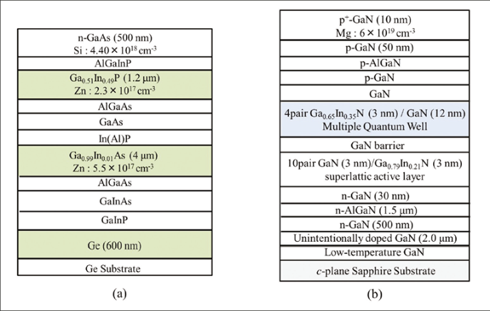
Figure 1. Higher solar efficiencies are promised by combing an (a) GaInN solar cell and an (b) GaInP/GaInAs/Ge three-junction solar cell.
For the multi-junction epiwafer, we used active layers of germanium, Ga0.99In0.01As and Ga0.51In0.49P with thicknesses of 600 nm, 4 μm and 1.2 μm, respectively. For this structure, grown on a germanium substrate, we employ top layers of n-type GaAs with a silicon concentration of 4.4 × 1018 cm-3.
One of the pre-requisites for realising a highperformance multi-junction solar cell is to ensure that each cell generates the same current density. This requirement dictates that the GaInN solar cell, which has an absorption wavelength of 530 nm, should have a thickness of at least 100 nm. Such a cell is yet to be developed, so we had to use GaInN solar cells and three-junction solar cells that are not current-matched, so that we can demonstrate the capability of waferbonding with this class of four-junction cell.
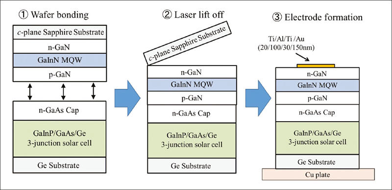
Figure 2. Wafer bonding can be used to fabricate GaInN/GaInP/GaInAs/Ge four-junction solar cells.
To fabricate our four-junction solar cells by waferbonding (see Figure 2), we first separate the sapphire substrate from GaN by laser lift-off. Success hinges on having a sufficient bonding strength.
We have found that the optimal conditions for forming a strong bond over a large area are to apply a pressure of 500 N at 450°C for an hour. Using these conditions, our experiments show that we can bond n-GaAs and p-GaN over 95 percent of the potential area and realise a bonding strength – as per tensile testing – of 4.5 MPa.
This value for the bond strength is very encouraging. It exceeds that of Au/Au junctions formed by wafer bonding, which have a typical value of 3.3 MPa. Given that those junctions have sufficient strength for the laser lift-off process, we are confident that our GaN/GaAs junctions will withstand the removal of sapphire by laser lift-off.
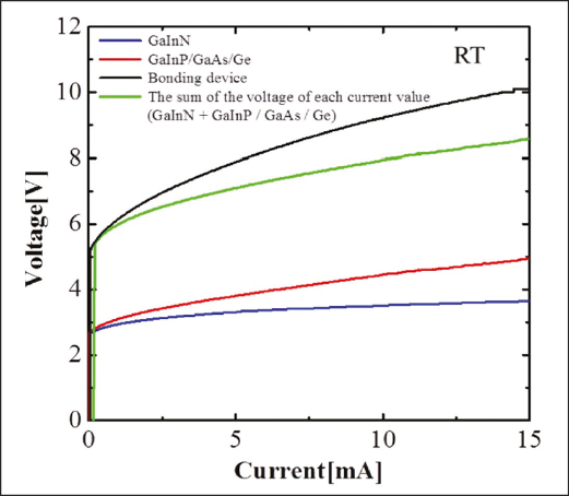
Figure 3. Current–voltage characteristics in the forward direction show that, as expected, the addition of the GaInN solar cell increases the turn-on voltage of the device.
To complete the fabrication of our four-junction device, we use inductively couple plasma, reactive-ion etching to remove the buffer and undoped GaN layers and expose GaN, and on this we form an electrode with a diameter of 110 μm (the electrode is a metal stack of Ti/Al/Ti/Au, with thicknesses of 20, 100, 30, and 150 nm, respectively). We form a second electrode on the n-type Ge substrate by bringing it directly into contact with a copper plate. Testing revealed that both electrodes have satisfactory ohmic characteristics.
So that we can benchmark the performance of this novel device, we also fabricated a GaInN solar cell and a GaInP/GaAs/Ge three-junction solar cell. All devices have been evaluated using radiation from an AM 1.5 G solar simulator, at room temperature and under a concentration of 1 sun.
The current status
In theory, the voltage at each injection current for our four-junction cell solar cells should equal the sum of the voltages at each current injection of the GaInN solar cell and three-junction solar cells (see Figure 3). Encouragingly, that is the case at a low current density, with the built-in voltage of the four-junction cell in close agreement with the calculated value. However, the voltage for the four-junction solar cell increases with the operating current, suggesting that although there is not a large Schottky contact at the junction interface, there is a large resistance at the bonding interface.
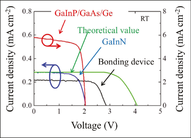
Figure 4. Solar cell characteristics under AM 1.5 G (1 sun) irradiation reveal that the bonded, four-junction device does lead to an increase in output voltage. However, this increase is not as high as it should be, due to imperfections at the interface between the p-type GaN and the n-type GaAs layers.
According to theory, in a multi-junction cell, the opencircuit voltage should be the sum of the values for each device, while the short-circuit current density should be a function of the device having the lesser value. In Figure 4, these theoretical values have been plotted for the four-junction, GaInN, and three-junction solar cells at 1 sun irradiation, assuming that the fill factor is the smallest possible value for each device. The open-circuit voltage, short-circuit current density, fill factor and conversion efficiency of each device is summarised in Table 1.

Table 1. Characteristics of each device
Also plotted in Figure 4 is the measured performance for our bonded device. The good news is that the open-circuit voltage of the solar cell increases with the addition of GaInN, verifying that a series connection has been formed with wafer bonding. However, this voltage lags the ideal value by about 1 V. Forward current–voltage characteristics could not reveal a large Schottky barrier, so the moist likely culprit is the junction interface.
To form our device, we have bonded p-type GaN and n-type GaAs. If the device is to operate in an ideal manner, there must be a low-resistivity tunnel junction in the bonding layer – but this might not be possible. What is possible, however, is to optimise the impurity concentration of the p-type GaN and n-type GaAs layers.
Measurements of the short-circuit current density show that this is slightly less than the ideal value. The sub-optimal value may originate from process damage, such as from laser lift-off and bonding interface effects. We are yet to identify the cause, and one of our next goals is to optimize the bonding interface and achieve a higher performance.
What we have shown is that wafer bonding technology can overcome the great hurdle of the large lattice mismatch between different crystals, and unlock the door to the fabrication of structures with many junctions. Once this process is optimised, it should lead to new records for solar cell efficiency, and ultimately help our world to meet the energy needs of tomorrow.
Further reading
K. A. Bertness et al. Appl. Phys. Lett. 65 989 (1994)
T. Takamoto et al. Prog. Photovolt: Res. Appl. 13 495 (2005)
A novel growth process, which forms thin, high-quality layers of GaN on graphene, promises to slash substrate costs and open up new device architectures by can Bayram from the University of Illinois at Urbana-Champaign
As regular readers of this magazine know, III-V compound semiconductors are leaving an indelible imprint on humanity. These materials are used to make LEDs, laser and amplifiers – and these devices are lighting our homes, offices and displays; reading our DVDs and Blu-ray disks; and increasing the communication speeds through wireless and wired connections.
The emergence of this multi-billion-dollar industry can be traced back to the 1950s, when extensive studies of GaAs first began. Since then, there has been diversification of materials, with InP research and development taking off in the 1970s, followed by the addition of GaN in the 1990s.
Judged in terms of intrinsic characteristics, GaN, along with its related alloys, is undoubtedly the most promising material system. By tuning the composition of the quaternary InAlGaN, the emission wavelength of the material can span from the deep ultraviolet to the near-infrared; and by subband-energy engineering of AlGaN/GaN superlattice quantum structures, the optical capability of this material can stretch to the terahertz regime. When it comes to electronics, GaN-based compound semiconductors can combine a large bandgap – it is 3.4 eV for GaN and 6.2 eV for AlN – with a high critical electric field strength, typically 106 V/cm, and high saturated electron drift velocities. Devices are no slouches either: AlGaN/GaN transistors that sport a two-dimensional electron gas are capable of cut-off frequencies in excess of 300 GHz.
However, GaN devices do have an Achilles heel: there is no lattice-matched, low-cost, high-quality substrate. Free-standing GaN can be formed, but not by the crystal growth methods used to make GaAs and InP, and the substrates that result are limited in size and quantity, riddled with imperfections, and very pricey.
Consequently, many devices are grown on foreign substrates that have a symmetry that is similar to that of GaN. Popular choices are sapphire, 4H-SiC, and silicon (111). Deposition of the GaN often occurs by MOCVD, with gallium and nitrogen introduced to the growth chamber in the form of a metal-organic compound and ammonia, respectively. When these materials impinge on the heated substrate, they decompose, and a mix of ionic and covalent forces drive the formation of GaN epilayers.
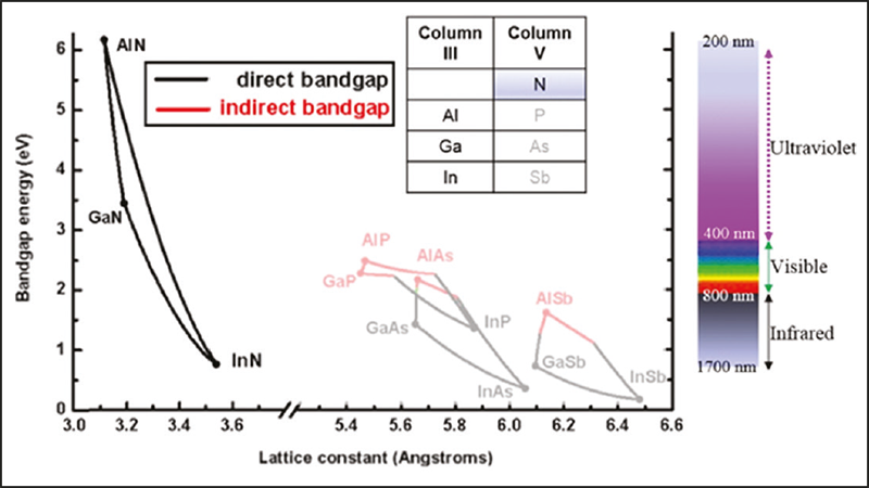
Figure 1. Bandgap energy versus lattice constant plot for III-V materials. The direct bandgap nature of III-nitrides enables emission tunability from ultraviolet to infrared wavelengths, making them one of the most promising materials for photonics.
While the resulting material is good enough for making commercial devices, it is far from ideal. When GaN is deposited on sapphire, 4H-SiC, and silicon (111), there are lattice-mismatches of 14 percent, 3 percent, and 17 percent, respectively (see Table 1), that lead to threading dislocation densities in excess of 108 cm-2. These imperfections act as non-radiative recombination centres, pegging back the efficiency of LEDs, lasers, transistors, and terahertz oscillators.
Fortunately, there is a low-cost, highly promising solution: van der Waals growth of GaN on graphene, a one atom-thick carbon chain that is cheap, scalable, and abundant. Our team at the University of Illinois at Urbana-Champaign is pioneering this approach, and has succeeded in being the first group to grow single-crystalline single-phase large-area GaN films on graphene by van der Waals epitaxy.
This form of epitaxy is markedly different to that of MOCVD. The starting point is the same – ammonia and a metal-organic compound are the reactants – but growth relies on the weak atomic forces between the gallium, nitrogen and carbon atoms. Due to this, van der Waals forces dominates the material deposition rather than much stronger ionic or covalent forces.
One of the great strengths of van der Waals epitaxy is that such weak interaction between GaN and carbon drastically relaxes the lattice-matching condition usually encountered in heteroepitaxial growth. The upshot is tremendous freedom in the combination of materials for forming heterostructures. This opens the door to a new way of fabricating novel heterostructures, using ultrathin superconducting, metallic, semiconducting or insulating films of layered materials as constituents.
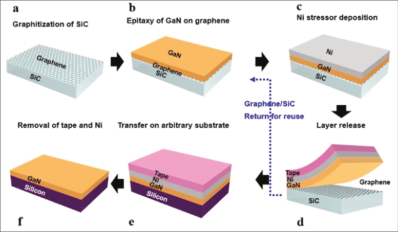
Figure 2. Researchers at UIUC have pioneered a method for growing/transferring single-crystalline thin films on/from epitaxial graphene. (a) Graphitization of a SiC substrate to form epitaxial graphene. (b) Epitaxial growth of GaN on graphene. (c) Deposition of a stressor layer (Ni). (d) Release of GaN from the substrate with a handling tape. (e) Transfer of the released GaN/Ni/tape stack on a host substrate. (f) Removal of the tape and Ni by thermal release and wet etching, leaving a GaN film on the host substrate. (adapted from adapted from J. Kim et al. Nature Communications 5 4836 (2014) and references there within).
By drastically relaxing the lattice-matching condition, van der Waals epitaxy offers much promise on many fronts. Its potential is not limited to just fulfilling the role of an epitaxial seed and release layer for subsequently-grown layers. If graphene is sandwiched between two other semiconductors, such as SiC and GaN, there is the potential to make hot electron transistors that are suitable for high-frequency, highspeed current switching applications. Calculations by Xiangfeng Duan’s group at UCLA suggest that hot electron transistors formed by the combination GaN-graphene-GaN can realise operation at 1 THz. Meanwhile, on the photonic side, when bi-layer graphene is sandwiched between wide bandgap materials, it possesses a bandgap of around 200 meV, an attribute that could aid the production of modulators. And in addition to these more esoteric devices, the pairing of GaN and graphene could form vertical GaN transistors, such as high-speed, highpower HBTs; and LEDs.
Despite this tremendous promise, van der Waals epitaxy of GaN materials on graphene – or any other two-dimensional material for that matter – has been almost unexplored until recently. That’s because much effort has been directed towards conventional materials and their heterointegration.
Encouragingly, dangling bonds were not needed for initial success, with van der Waals epitaxy enabling the direct deposition of a layered material onto a cleaved face of another layered material. And more recently, van der Waals epitaxy has been possible with the deposition of two-dimensional semiconductor structures on both two- and three-dimensional semiconductors, with the process driven by the formation of mixed atomic bonds.
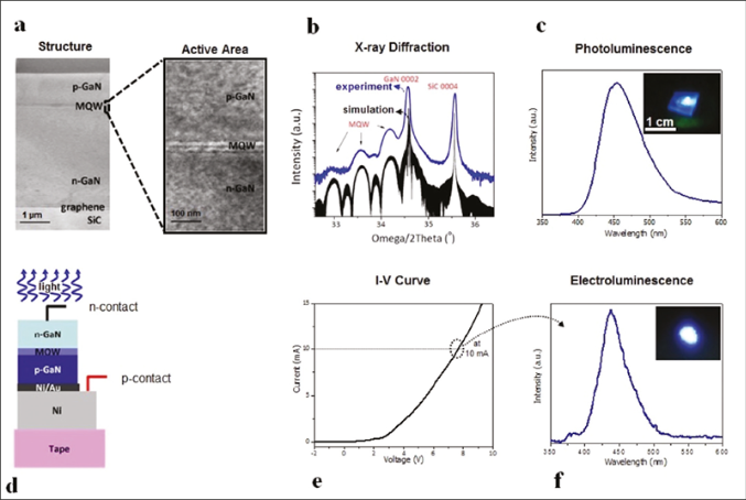
Figure 3. Thin-film blue LEDs via GaN-on-graphene technology. (a) Cross-sectional transmission electron microscopy image of LED stacks (p-GaN/MQW/n-GaN) on a graphene/SiC substrate (scale bar, 1 μm) and high-resolution transmission electron microscopy magnified the multi-quantum well (scale bar, 100 nm). (b) High-resolution X-ray diffraction/simulation data from the InGaN/GaN LED heterostructure grown on a reused graphene/SiC substrate. (c) Photoluminescence data from the InGaN/GaN LED heterostructure grown on a reused graphene/SiC substrate. The picture of the LED-emitting blue light is displayed in an inset. (d) Schematic of a transferred visible LED device on the tape. (e) Current-voltage characteristics of a transferred LED stack measured by applying positive bias on nickel and negative bias on n-GaN. (f) Electroluminescence spectra of a transferred LED stack taken at 10 mA injection. The picture of the LED-emitting blue light is displayed in an inset.
However, when it comes to the growth of threedimensional semiconductors on two-dimensional semiconductors, it’s been a different story. These efforts, typically associated with the likes of three-dimensional CdS and CdTe on two-dimensional graphene, MoTe2, and WSe2, tend to suffer from many weaknesses. They include: structural metastability, that is, phase-mixing; chemical metastability, such as a tendency toward spinodal decomposition; and in some instances, including that of GaAs, chemical incompatibility. The root causes are that growth requires elevated temperatures and complex precursors.
Due to these impediments, growth tends to form oriented clusters of polycrystalline material with a grain size of less than 100 nm. These grains are so small that they render this technology useless for the production of substrates and devices. Note that the insertion of an intermediate layer, such as ZnO in-between a compound semiconductor and a twodimensional layered substrate, is not a great solution. That’s because it results in low-quality heteroepitaxy, and leads to a partial film coverage at best.
The way forward is to directly deposit a threedimensional semiconductor on a two-dimensional material through a form of van der Waals epitaxy. We have pioneered this using epitaxial graphene as the platform. Epitaxial graphene is enabled through sublimation of a SiC substrate at high temperatures, typically more than 1600 °C). Silicon diffuses out, and the remaining carbon atoms rearrange to enable a self-terminating monolayer graphene, called epitaxial graphene.
Regrowth of GaN on such graphene requires a new epitaxial approach. Instead of inserting a conventional buffer layer at a low temperature of typically 500-700 °C, similar to what have been done conventionally between highly mismatched materials, we employ a high temperature buffer layer at around 1100 °C. Raising the temperature ensures better coverage of the graphene nucleation surface with the buffer layer – and when the subsequent growth of GaN takes place, initiated from the graphene facets, heteroepitaxy evolves properly.
One of the strengths of this GaN on epitaxial graphene approach is that the weak, quasi van der Waals forces between GaN and graphene offer a convenient means for substrate-scale release. This could aid efforts associated with the fabrication of thin, large-area vertical GaN devices as well as reuse of the expensive SiC substrates.
Our technology has led to the growth, on epitaxial graphene, of GaN films with a root-mean-square roughness of 3 Å and a defectivity as low as 4 × 108 cm-2. We have also been able to transfer entire single-crystalline GaN films on to an arbitrary substrate (see Figure 2).
What’s more, because graphene is flat, so is the released interface – it has a root mean square roughness of just 5 Å. Thanks to this, we have been able to form adhesive-free, GaN-on-silicon structures that are ideal for the production of hybrid GaN-onsilicon (100) devices. By re-using the graphene/SiC substrate, we have been able to undertake multiple growth and transfer cycles of GaN films.
One of the key milestones in our work has been the growth of InGaN/GaN epitaxial LED stacks on a recycled graphene/SiC substrate – it has been reused three times. The fully-functional flexible blue LEDs that we have demonstrated (see Figure 3) are ultra-light and are capable of conforming to curved surfaces.
A major implication of our work is that it has the potential to address one of the biggest challenges facing many forms of GaN power devices, including RF transistors: heat extraction. Our ultra-thin GaN technology allows us to optimize the passive cooling of GaN HEMTs and reduce the junction temperature by around 50°C for 8 W of dissipated heat. Given the exponential relationship between the junction temperature and lifetime, such passive cooling through thickness optimization creates an opportunity for improved output power and reliability.
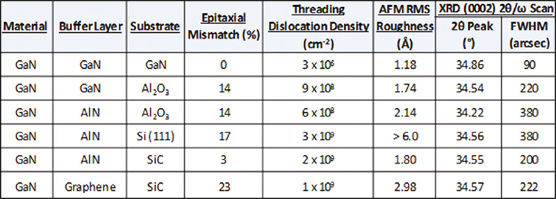
Table 1. Comparison of crystalline quality of GaN grown on various substrates (adapted from J. Kim et al. Nature Communications 5 4836 (2014) and references there within).
Our results pave a promising path for the development of III-nitride semiconductors, by enabling the integration of these devices with other semiconductors. Further progress hinges on realising a better understanding and greater control of GaN epitaxy on graphene, so that it is possible to produce single-crystalline, wafer-scale GaN material with low defectivity on a scalable graphene platform.
Where we have led, many others will follow, each taking a different path. There are more than five hundred two-dimensional materials, and it is safe to predict that this century will depend as much on twodimensional materials as the last century depended on three-dimensional ones.
Part of this work, carried out in the Micro and Nanotechnology Laboratory and Frederick Seitz Materials Research Laboratory Central Research Facilities, University of Illinois at Urbana-Champaign, IL, USA., is based upon work supported by the Air Force Office of Scientific Research Young Investigator Program under award number FA9550-16-1-0224. Part of this work, carried out at IBM Watson Research Center, NY, USA, was in collaboration with chief collaborator J. Kim (now at Massachusetts Institute of Technology, MA, US) and fellow scientists H. Park (now at Kyungpook National University, Daegu, Korea), C.-W. Cheng, C. Dimitrakopoulos (now at University of Massachusetts Amherst, MA, US), J. A. Ott, K. B. Reuter, S. W. Bedell, and D.K. Sadana.
Further reading
A. Koma Thin Solid Films 216 72 (1992)
J. Kim et al. Nature Communications 5 4836 (2014)
Le Huang et al. J. Phys. Condens. Matter 26 295304 (2014)
T. Loher et al. J. Appl. Phys. 80 5718 (1996)
K. Chung et al. Science 330 655 (2010)
Y. Kobayashi et al. Nature 484 223 (2012)
K. Park et al. Appl. Phys. Lett. 109 151904 (2016)
N. R. Glavin et al. Adv. Mater. 29 1701838 (2017)
Filling backside trenches with AlN helps to slash leakage currents
GaN HEMTs can now combine very high blocking voltages with incredibly low leakage currents, thanks to the efforts of engineers from the Institute of Electronics, Microelectronics and Nanotechnology in Villeneuve dAscq, France.
This team’s metal-insulator-semiconductor HEMT produces a 3 kV blocking voltage at a leakage current of less than 1 μA/mm.
Realising such a high blocking voltage is not, in itself, a recent breakthrough for these engineers – they reported 3 kV HEMTs back in 2015. But those transistors had a leakage current of 1 mA/mm, three orders of magnitude higher than it stands today.
“1 mA/mm is not usable for high power devices from a practical point of view,” explains team leader Farid Medjdoub, who attributes the tremendous reduction in leakage current to improved processing and the use of thick PVD-grown AlN within the backside trenches.
Medjdoub – who is working within Inrel-Npower, a European Union Horizon 2020 project that includes On-Semiconductor – says that the next step on the road to commercialisation is the production of larger devices.
“This proof of concept has been performed on small devices, with a gate width of 100 μm,” explains Medjdoub, who says that efforts must now be directed at demonstrating devices with a total gate width of 10 mm or more.
The success that the team has had with smaller devices has been aided by contributions from other companies. Transistor fabrication began by processing 6-inch GaN-on-silicon epiwafers provided by EpiGaN. These wafers contain an AlN nucleation layer, AlGaN graded transition layers, an Al0.08Ga0.92N buffer layer, a 150 nm-thick GaN channel, a 20 nm Al0.25Ga0.75N barrier and a SiN cap, deposited in-situ.
Front-side processing followed, involving: the addition of Ti/Al/Ni/Au ohmic contacts, directly on the AlGaN barrier; device isolation by nitrogen implantation; deposition of a Ni/Au stack on the SiN cap to create metal-insulator-semiconductor structures; and a further deposition of 200 nm of SiN to provide additional passivation. To complete fabrication, the engineers locally etched the substrate up to the AlN nucleation layer, so that silicon is removed up to 50 μm away from the sidewalls, before adding a 15 μm-thick layer of AlN.
The latter step is undertaken by Kyma Technologies. “They had already experience with thick PVD deposition of high resistive AlN,” explains Medjdoub, “and deposition in their case can be performed on large wafer diameters.”
Electrical measurements on devices with a 50 μm gate width, 2 μm gate length, and a gate-to-drain spacing of 40 μm revealed the impact of the steps taken to form the novel architecture. Removing the silicon substrate cut the maximum current density from 8.8 mA/mm to 6.3 mA/mm, due to self-heating (there is inferior thermal dissipation in air, leading to a high channel temperature, a reduction in channel mobility and ultimately a decrease in the drain current). But once AlN has been added, followed by deposition of a 2 μm-thick film of copper that aids thermal conductivity, self-heating diminishes and the current density recovers to 85 percent of its original value.
An evaluation of three-terminal off-state leakage characteristics revealed a breakdown voltage of just over 3 kV for the team’s transistors, for an off-state leakage current of 1 μA/mm. Specific on-resistance is 13 mΩ cm2.
The engineers are currently evaluating larger devices. Preliminary tests are underway at On-Semiconductor, for power devices with a current rating in excess of 20 A.

Removing the silicon substrate enables an increase in blocking voltage, while the addition of AlN holds the key to a substantial reduction in leakage current.
Gallium oxide power devices grown by CVD trump those made from GaN and SiC
A team from the US is claiming that it has broken new ground by demonstrating the feasibility of low-pressure CVD for the growth of β-Ga2O3 vertical power devices.
“Using low-pressure, CVD-grown beta gallium oxide epitaxial films, we demonstrated Schottky barrier diodes with breakdown fields exceeding current GaN and SiC technology,” remarks team spokesman Chandan Joishi from Ohio State University.
According to him, the merits of low-pressure CVD include its low cost, its high growth rate, and its capability to produce uniform, high-quality films of β-Ga2O3 that have controllable doping.
He also points out that low-pressure CVD tools are widely available, because they account for more than one-third of the CVD market – and this growth technology is very compatible with existing process technologies used in the semiconductor industry.
One of the alternative growth processes for β-Ga2O3, HVPE, is capable of similar growth rates, but the tools are less mature. Another option is mist-epitaxy, a technique pioneered by Flosfia of Japan, but this offer less control over doping. According to Joishi, lowpressure CVD can provide a doping range of 1016 cm-3 to 1019 cm-3, while mist epitaxy is limited to 1017 cm-3 to 1019 cm-3.
There are several polytypes of Ga2O3, and the team from the US is working with the β-phase, due to its stability, plus the opportunity to form native, low defect density substrates with melt-based techniques. “This makes beta-gallium oxide substrates inexpensive compared with SiC and GaN, which are synthesized using unconventional approaches, by employing high temperature and pressure,” says Joishi.
He and his co-workers from The Ohio State University, The University of Utah and Case Western Reserve University have produced Schottky barrier diodes that feature a bevel design.
“Bevel designs are common for high-voltage powerrectifiers and thyristors,” says Joishi, who explains that this geometry enhances the breakdown voltage by reducing the field at the edge of the device.
Fabrication of Schottky barrier diodes began by taking substrates of tin-doped β-Ga2O3 (010) and cleaning their surfaces with acetone, toluene and isopropyl alcohol. The substrates were loaded into a horizontal reactor, annealed at 900 °C under oxygen for 30 minutes, and coated with a 2 μm-thick film of β-Ga2O3.

A bevel design with field plates promises to cut the strength of the peak electric field in Schottky barrier diodes.
The next device fabrication step involved using an electron-beam evaporator to deposit Pt/Au/Ni and Au/Ni stacks, which formed the anodes and cathodes, respectively. After this plasma etching defined the trench, SiO2 was then deposited conformally by plasma-enhanced CVD. Finally, the oxide over the anode was etched away so that subsequent sputtering of titanium could create a device with a field plate overlap of 4 μm.
Comparing measurements on completed devices with those only partially processed revealed that trench etching increased the on-resistance from 3.6 mΩ cm2 to 6.7 mΩ cm2. This is attributed to surface damage, which is not repaired by passivation.
Trench etching was also detrimental to the breakdown voltage, which fell from 138 V to 74 V. However, adding field plates led to an overall improvement in this figure, with the blocking voltage rising to 190 V – and this refinement increased the forward current density to more than 1 A cm-2.
Joishi and co-workers are planning to increase the growth rate for β-Ga2O3 films, and decrease the background doping in these layers. Success will aid efforts to make devices with a β-Ga2O3 layer that is more than 100 μm-thick, and has a low background doping.
“Suitable field management will be used to realise beta-gallium-oxide Schottky power devices exhibiting a higher breakdown of up to 10 kV, low resistance and [low] switching loss,” explains Joishi.
Reference
C. Joishi et al. Appl. Phys. Express 11 031101 (2018)
Electroluminescence uncovers the extent of current collapse in GaN HEMTs
GaN HEMTs are held back from fulfilling their promise as devices that can deliver unprecedented power, speed and efficiency by a malady known as current collapse – the temporary, recoverable reduction of current following an electrical stress.
To understand the cause of current collapse and ultimately address this weakness, researchers have turned to electroluminescence spectroscopy to identify high-field regions where premature breakdown within the device is most likely to occur. Recently, this technique has been taken to a new level by a team from the University of Fukui, Japan.
“We have demonstrated that electroluminescence analysis is a powerful tool not only for identifying regions of high electric field, but also for visually assessing the degree of current collapse, which is a long standing problem in AlGaN/GaN HEMTs,” says team spokesman, Joel Asubar.
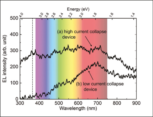
HEMTs with bright whitish electroluminescence near the drain contact suffer from severe current collapse (a), while those producing faint reddish electroluminescence across the entire gate-drain access region show significantly suppressed current collapse (b).
One key finding by the team is uncovering a tell-tale sign for severe current collapse: the emission of bright whitish electroluminescence near the drain contact.
“Devices with faint reddish electroluminescence across the entire gate-drain access region show significantly suppressed current collapse,” adds Asubar.
The team’s studies of current collapse – caused by the trapping of electrons that locally deplete the conductive two-dimensional electron gas – have been made on four forms of GaN HEMT. These devices, all containing a 25 nm-thick AlGaN barrier, feature: SiN passivation; SiO2 passivation; SiN passivation, followed by oxygen plasma treatment; and SiN passivation on a HEMT capped with GaN.
To passivate the device, the team deposited either a 150 nm-thick layer of SiN or a 140 nm-thick layer of SiO2 on top of the AlGaN barrier. The variant with a cap contained a 2 nm-thick layer of GaN, while that subjected to oxygen plasma treatment underwent exposure to a 100 W source for one minute.
Asubar and co-workers evaluated the degree of current collapse in the four different types of transistor with on-wafer pulsed measurements. Using an offstate drain bias of 100 V and a train of gate pulses between -5 V and 1 V, they determined the dynamic on-resistance – and by dividing this by the static onresistance, they produced a value for the normalised dynamic on-resistance.
When passivation had not been combined with any other scheme for improving device performance, values for the normalised dynamic on-resistance were 700, indicating a high degree of current collapse. Electroluminescence from these devices, using source-drain voltages of 600 V to 1 kV, had a high intensity whiteish peak, emitted near the drain contact.
Combining oxygen plasma treatment with SiN passivation produced a normalised dynamic onresistance of just 33, while adding a GaN cap prior to SiN passivation produced a value of 158. In both cases, devices produced a low-intensity reddish electroluminescence spectra across the entire gatedrain access region.
The team claims that the electroluminescence characteristics produced by their HEMTs are governed by the density of trapped electrons, which is highest near the drain region of devices with the higher normalised dynamic on-resistance. When the drainsource voltage across these transistors increases, more electrons are injected and trapped, leading to further movement of the high-field region in the drain direction – and once the electric field near the drain contact is very high, electron energy is also very high, leading to wide electroluminescence spectra.
Although the researchers have shown that electroluminescence can assess the degree of current collapse in GaN-based transistors, they don’t expect this technique to be employed in device production, due to its almost destructive nature.
“Nevertheless, if the reward of such electroluminescence tests – such as getting useful information about electrically weak points and current collapse – can outweigh the cost penalty, it can be given serious consideration,” argues Asubar.
One of the team’s next goals is to prepare devices with intentionally-designed irregularities, to investigate their effect on device electroluminescence and breakdown. “This may help us identify electrically weak points and therefore help us design an optimum electrode shape for improved breakdown characteristics,” says Asubar.
Reference
S. Ohi et al. Appl. Phys. Express 11 024101 (2018)
