

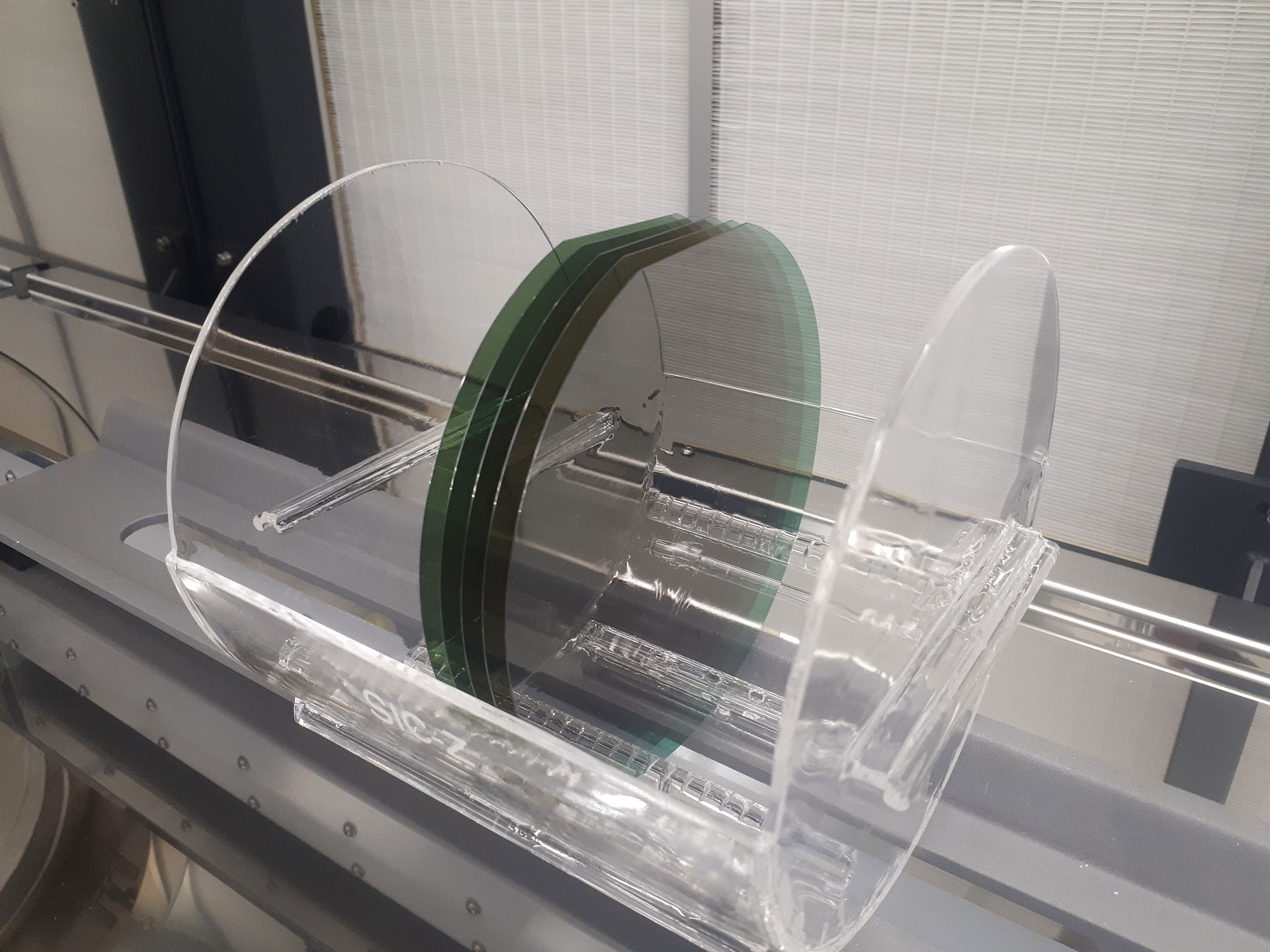


MANY OF US view the GaAs VCSEL as an established product and its GaN-based cousin as a project in the lab. But the reality is more nuanced.
While the GaAs-based VCSEL has enjoyed some great success – it made its named in short-reach interconnects for data coms, and now has a new lease of life in facial recognition systems in top-of-the-range smartphones – it continues to evolve. The latest killer application has fuelled a ramp in volume, due to the need for an array of emitters rather than a single source, and this has driven the development of a new design. As production has shifted from 50 mm and 75 mm substrates to those with a diameter of 150 mm, to cater for the increase in real estate of the emitters, this has introduced issues; and alongside that, a novel solution.
For many, it will come as a surprise that there is an issue, given that the fabrication of the GaAs VCSEL is relatively easy, thanks to the pairing of GaAs and AlAs. These two materials appear to be an ideal combination, having very similar lattice constants but markedly different refractive indices, traits that enable the growth of high-quality mirrors that provide the optical feedback in this class of laser. But for the latest, larger epiwafers, even the small degree of strain that comes from a minimal mismatch between GaAs and AlAs is enough to distort epiwafers grown on GaAs and hamper downstream characterisation and processing.
Addressing this issue is the global epiwafer manufacturer IQE. Engineers at its facility in Cardiff, UK, have switched substrates, moving to germanium, which has a lattice mismatch straddling that of GaAs and AlAs. Trials have shown that on 150 mm substrates, distortions to the shape of the epiwafer fall by an order of magnitude compared with the incumbent . Results on prototype devices are also encouraging, leading IQE to offer this form of epiwafer as a commercial product. Variants on 200 mm germanium wafers are set to follow.
While GaN-based VCSELs are lagging behind their GaAs-based siblings, they are catching up. Although confined to the lab, the leading development of these lasers is taking place at some of the biggest compound semiconductor chipmakers in Japan, using processes that are compatible with high-volume production.
Leading the way is Nichia, with milliwatt emitters sporting record-breaking efficiencies in the green and blue. Efforts are motivated by producing these devices for colour-projectors in smart glasses, where they should ensure a long battery life and eye safety.
Nichia played a major role in early GaN-based VCSEL development, and its latest success has come from replacing a pair of dielectric mirrors with one of these, alongside another from lattice-matched GaN and AlInN. This combination is a common approach for the mirrors, which are, without doubt, the most difficult part of the VCSEL to produce.
It is clear that optimising the GaN-based VCSEL will take some time. Its GaAs-based cousin is clearly far closer to that goal, but even it has a little way to go.
Above: China’s first vertically integrated SiC line at the Changsha high-tech industrial park.
IN JUNE THIS YEAR, China-based Sanan Integrated Circuit (Sanan IC) opened the nation’s first vertically integrated SiC line at its Hunan Sanan Semiconductor plant. Located in the Changsha high-tech industrial park in the Hunan province, Sanan IC’s latest manufacturing fab with a $2.5 billion investment, has, so far, taken less than a year to build and handles all wafer and device fabrication steps from crystal growth to power devices, packaging and testing.
“This is phase 1 of our site,” highlights Mrinal Das, Director, Technical Marketing and Sales at Sanan IC, which alongside Hunan Sanan, is a subsidiary of Sanan Optoelectronics. “At 15,000 wafers a month, we’ve brought half of its full capacity online... In phase 2 we will build a mirror image of phase one.”
“We have an aggressive plan to get the plant fully operational – meaning equipped to deliver 30,000 wafers a month by 2024,” he adds.
From here on in, Sanan IC’s Changsha megafab will be delivering a mix of wafers and devices to both domestic and international customers. Describing the site as Sanan IC’s ‘captive’ wide bandgap power semiconductor facility, Das won’t be drawn on actually supply figures right now other than to say the facility is currently ‘15K a month capable’.
Built to churn out six-inch SiC wafers, Das also expects to see eight inch wafers being produced come 2024. As he puts it: “My vision is that during phase 2, if there is enough demand, we will work on eight-inch wafers so that in 2024 we could probably [be producing] 15,000 six-inch and 15,000 eight-inch wafers.”
“After that, and if demand continues to rise in the next five to ten years, we will scale phase one and increase capacity to 30,000 eight-inch wafers every month,” he says. “Our crystal growth team has put a lot of effort into our [wafer] technology and we have invested in innovation through our patent filings in China and the US.”
Indeed, Sanan IC has been manufacturing SiC Schottky diodes for some time now and also has SiC MOSFETs under qualification – 1200 V devices are scheduled to be released soon. According to the Sanan IC Director, the figure of merits for substrates, epitaxy and devices are all ‘achieving parity’ with industry-best technology.
Das is keen to emphasize that the organization also makes GaN-on-silicon devices for lower-power applications. And as his Sanan IC colleague, Raymond Biagan, Senior Director, Sales and Marketing Communications – North America and Europe, highlights: “Our business model is to offer our entire manufacturing platform to the worldwide market.”
In the interim, Sanan Hunan will hire engineers locally and from further afield. Engineers will predominantly come from a pool of domestic talent, but there will also be a portion of technologists from Taiwan, Japan and elsewhere.
Market competition
Still, Sanan IC and its Hunan Sanan Semiconductor plant are hardly operating in a vacuum. Recently, Cree, US, has poured $1 billion into its 200 mm SiC fabrication facility in Mohawk Valley, New York, while Rohm of Japan has just finished building its $190 million SiC wafer and device fab in Chikugo, Japan. US-based II-VI also intends to plough up to $50 million into its China SiC substrate manufacturing capacity and Infineon of Germany is set to increase SiC epitaxy wafer production.
However, Das – who worked at Cree and Wolfspeed for more than 16 years – reckons Sanan’s China-based megafab gives the organisation an edge.
“Wolfspeed, for example, has the biggest news on capacity expansion so far with their materials supply stretching from North Carolina to upstate New York, and with packaging typically at various outsourced semiconductor assembly and test companies across Asia,” he says.
“But while Wolfspeed is vertically integrated there is still this logistical challenge of moving their product through various stages globally, whereas we have a nice, compact, single site that will do everything,” he adds.
Both Das and Biagan believe the Changsha site also sets up their company to more easily target the all-important electric and hybrid electric vehicle markets, in China.
“Analysts indicate that the hockey stick for wide bandgap materials will be automotive markets, so it’s been natural to headquarter in China where we can cater for its large automotive market, in terms of logistics and quick time to market.” says Biagan. “Our parent company, Sanan Optoelectronics, is already a major supplier of LED chips and car lamps to the automotive industry here, and we can further appeal to that marketplace by delivering SiC and GaN domestically.”
Das and Biagan are also confident the burgeoning SiC industry has enough room for everyone. Das points out that the true competitor for all SiC players is silicon, and he and colleagues at Sanan IC hope to work alongside the competition to enable the widespread adoption of wide bandgap materials.
Still as Biagan puts it: “Our aspiration is to be considered a major market shareholder in the SiC space that is today served by companies such as Wolfspeed and STMicroelectronics, and to be known as a viable brand for wide bandgap materials and devices globally.”

Making SiC wafers at Sanan IC’s Hunan Semiconductor.
Above: Akhan Semiconductor engineers holding their 300 mm diamond wafer
IN A VERY SHORT space of time US-based Akhan Semiconductor has signalled a clear intent to massively scale up production of its synthetic, lab-grown electronics-grade diamond materials. In late June, former president of Intel Americas, Tom Lacey, joined the company board as chairman. The semiconductor executive has also spearheaded start-ups, mid-sized and larger public and private companies, and as he says: “Now is the time to unleash diamond’s immense capability on chips, as well as optical and glass coatings.”
Then, only a few weeks later, Akhan revealed it had fabricated 300 mm diamond CMOS wafers at its production facility, northern Illinois Diamond Mine 1. As Adam Khan, company founder, puts it: “From a commercial standpoint, 300 millimetre is the standard, and we want to show that we have these processes that can form even the most advanced chips.”
“We’ve transitioned from laboratory innovations to repeatable and massively scaleable processes,” he adds. “With Tom, we’re moving from an entrepreneurial phase to operational growth... We want to license our materials to fabs and end-customers worldwide so they can incorporate these into their chip designs.”
Early days
Khan founded Akhan Semiconductor back in late 2012, confident that diamond could deliver excellent display glass properties for smartphone screens and optical performance for mirrors and lenses. He was also certain that diamond semiconductors could replace silicon devices and outperform wide bandgap materials, including GaN and SiC.
Partnering with Argonne National Laboratory, Akhan obtained exclusive rights to license the centre’s diamond CVD technology, which enabled nanocrystalline diamond film deposition onto wafer materials at temperatures as low as 400 °C. Combined with Akhan’s co-doping method – in which devices are doped with phosphorus and nitrogen, and then doped with boron or lithium to engineer atomic distribution – the pairing looked set to fulfil Khan’s hopes.
As Argonne Materials Scientist, Anirudha Sumant, said at the time: “This licensing agreement gives us the impact of a one-two punch, in which we combine Akhan’s novel process to achieve efficient n-type doping in diamond with Argonne’s low-temperature diamond deposition technology... This will break barriers that restricted the use of diamond thin films in the semiconductor industry to only p-type doping.”
Fast forward to today and this approach has been a success. Akhan has filed more than 40 patents worldwide, supplied its technology to Lockheed Martin, an unnamed smartphone OEM and other key industry players, and has now demonstrated the manufacture of 300 mm CMOS diamond wafers.
According to Khan: “We’ve done this using hot filament CVD [widely used to deposit diamond films] and get exceptionally high yield... the rejection rate has been less than 10 percent with wafers being rejected due to edge-to-edge film variability rather than tolerance.”
“This is a robust, scaleable process but 300 millimetre is not our maximum size – we can grow diamond on panels even larger than this,” he adds.
The company works with an impressive range of substrates, including silicon, glass, fused silica, sapphire, SiC, GaN and other crystalline semiconductor materials, and refractory metals. Devices for automotive applications are being fabricated on either silicon or SiC substrates.
“We have patents and ‘trade secret’ processes for each material, including how we prepare the material, growth conditions and post-processing,” says Khan. “The seed material and chemicals used to functionalise this vary by material type, and also by material thickness, roughness or finish.”
As the Akhan founder also points out, the material’s crystal size is altered depending on the applications – for example, a large grain polycrystalline material enhances carrier mobility for high-power, high-frequency applications. “We haven’t seen the need to develop single crystal [materials] for the applications we’ve pursued, as what we are seeing is already so much better than SiC and GaN,” he says.
Indeed, along the way, Khan and colleagues have been tracking SiC and GaN developments in the RF power sector, and fabricating MOSFETs, MESFETs, bipolar and CMOS structures that bring unprecedented power densities to this application.
“We demonstrated a working diode back in 2013 and are currently deploying technologies with Lockheed Martin... [this includes] a joint effort with our diamond-based electronics and optics on their F-35 platform,” highlights Khan.
Performance-wise, Khan says power density of his diamond semiconductors beats that of GaN and SiC, exceeding 40 W/mm, while carrier mobility hits many hundreds of cm2 V-1 s-1. Patent detail indicates a monolithically integrated diamond semiconductor to have conduction electrons with a mobility exceeding 770 cm2 V-1 s-1 at 300K. “We know it’s quite fast in terms of switching,” says Khan.
Khan also reckons his devices are cheaper, per dollar/cm2, than the GaN and SiC equivalent. “We only use a very thin layer of diamond – just enough for the active layer,” he says. “Then the substrate cost is just silicon – which is cheaper than GaN and SiC.”
So what now for Akhan Semiconductor and its diamond electronics? The company has historically delivered materials for aerospace and defence applications, but is now preparing to launch products into automotive applications.
“We’ve focused on this since 2012... we’re ready to start licensing our first technologies, including power inverters, and will have them in the [automotive] market by the 2021 time-frame,” says Khan. “Once the revenues are there for the automotive side, I think consumer electronics will be next.”
Smart Cut substrate technology charts a greener, faster and better path for the production of power electronic components
BY OLIVIER BONNIN, ERIC GUIOT, WALTER SCHWARZENBACH AND GONZALO PICUN FROM SOITEC
THIS YEAR has witnessed horrendous flooding in China and central Europe, along with soaring temperatures in north America. So it would appear that climate change is already underway, driven by rising levels of CO2 emissions. The prevailing view of the scientific community is that this situation is only going to deteriorate, and if the additional rise in temperature is not restricted to below 1.5 °C, our climate will undergo a substantial change.
Key to trimming CO2 emissions and staying within that limit for a temperature rise is sustainable development, which includes the introduction of greener technologies and processes. The industrial sector, electricity generation and transportation now accounts for about three-quarters of all CO2 gas emissions. So there is clearly a need to build a better, greener energy ecosystem. This can be realized by making substantial improvements on three fronts: slashing the energy consumed by data-centres, ramping renewable energy production, and accelerating the production of zero emission vehicles (ZEVs).
Within the ZEV sector, efforts must be directed at taking every opportunity to increase the power conversion efficiency, from electrical generation through to the provision of power at the powertrain. To excel in this endeavour, there must be a shift towards the use of greener power electronic components that deliver better performance and are made from more eco-friendly production processes.
Today’s incumbents, which are silicon-based components, are operating at their theoretical limit and cannot deliver the additional performance required for the more-efficient, greener systems needed for next-generation ZEVs. There must be a move to widespread adoption of wide bandgap semiconductors, such as SiC, which enable devices that combine higher operating temperatures with faster switching frequencies and higher efficiencies. Powertrains adopting this technology not only excel in efficiency – they are also smaller, lighter, and lower-cost.
Pioneering the uptake of SiC in ZEVs is Tesla. Back in 2017 it started deploying this technology in its Model 3 cars, importing power electronic components from STMicroelectronics. Where Tesla has led, others are sure to follow, creating a massive market for SiC, given that the ZEV market will account for more than half of all vehicle sales by the end of this decade, and all purchases come 2050 (see Figure 1).
Going hand-in-hand with this revolution in transportation, there needs to be a dramatic increase in renewable energy production. Humanity is heading in the right direction, with the installed capacity for producing energy from the sun and the wind expected to increase three-fold by 2040. In both these forms of renewable, the inverter is a key component.
Designers of this component are seeking reductions in volume and weight, alongside an increase in global system efficiency. To accomplish these goals, they will employ simplified bi-directional topologies, enabled by SiC, that handle more than 100 kW.
Hampering efforts to curb CO2 emission is the rapid growth in the IoT (Internet of Things) and AI (Artificial Intelligence). They contribute to global emissions by digital applications, a sector estimated to account for up to 10 percent of all emissions by 2025, and possibly more than 20 percent by the end of this decade. There is an urgent need for new data centres with smaller CO2 footprints. One way to realise this is to increase electrical power efficiency. For that, switching to a higher power density by introducing SiC is a valid option.
The Achilles heel of SiC
While SiC has many strengths, production of boules by the conventional technique, physical-vapour transport, requires temperatures of typically 2300°C to 2400 °C – this is far higher than that for silicon, which is grown at 1400 °C to 1500 °C. Additional drawbacks are that it can take a week to grow a SiC boule, and this only yields 40 to 50 wafers.
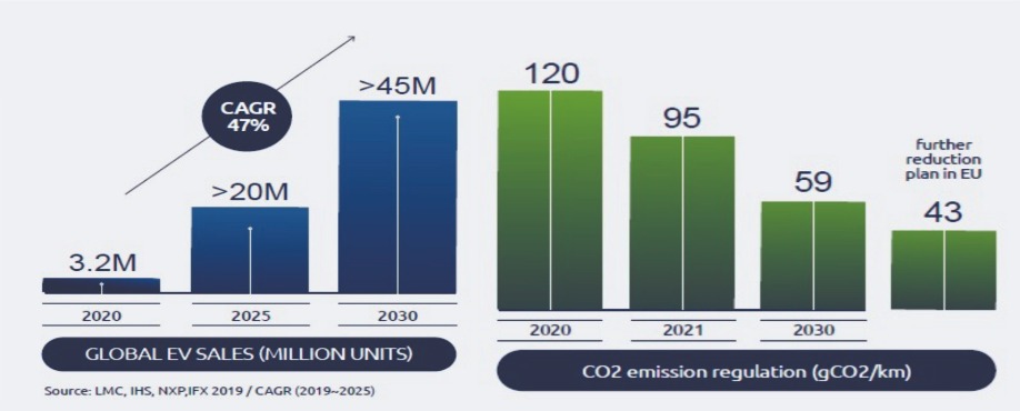
Figure 1. The fast transition towards EVs will be a key factor behind reductions in CO2 emissions. This transition will be accentuated by governmental regulations on gCO2/km.
At Soitec of Bernin, France, we have a solution to this problem: a proprietary layer-splitting and wafer-bonding technology, known as Smart Cut. Applying this to SiC allows a thin, monocrystalline layer of this material to be transferred from a SiC donor substrate to a SiC carrier substrate.
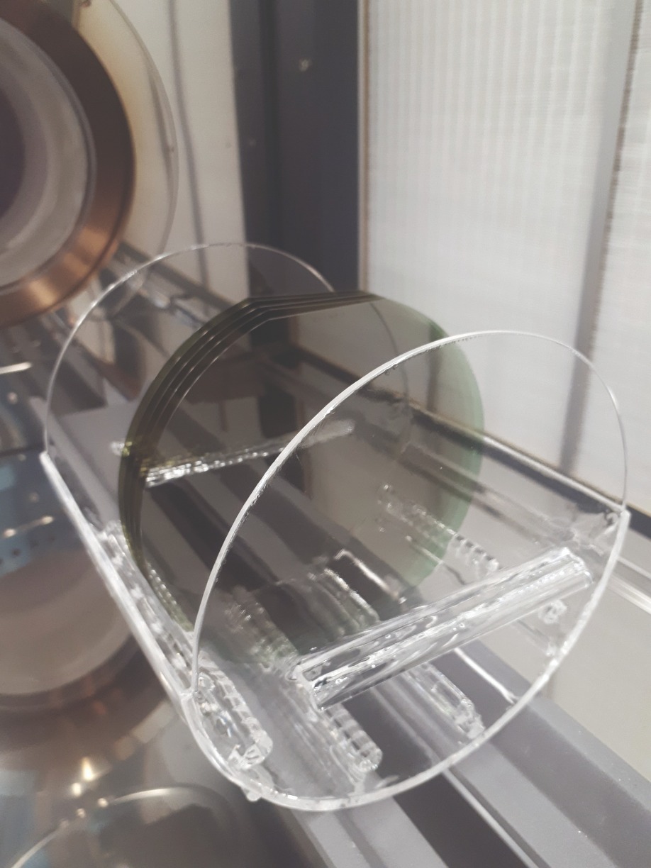
Soitec’s Smart Cut process, developed to reduce costs in the microelectronic industry, is poised to increase the competitiveness and volume of SiC devices.
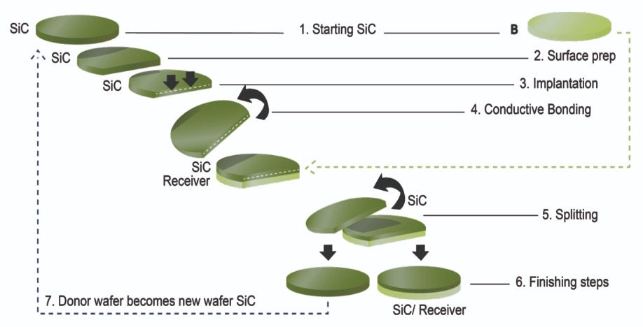
Figure 2. Soitec has adapted its Smart Cut process for the production of SiC.
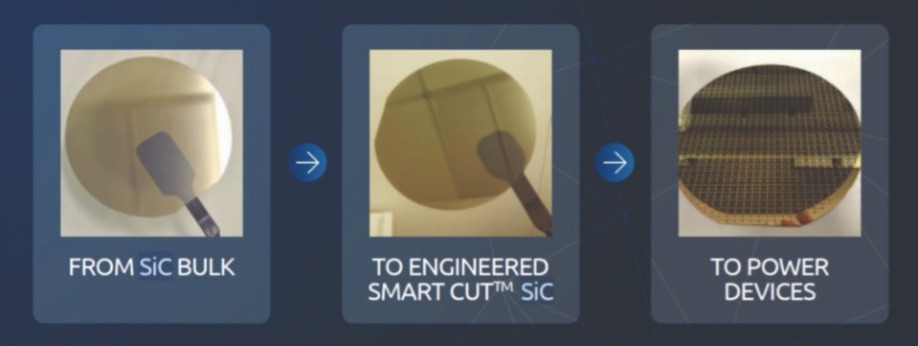
Figure 3. Pictures of bulk SiC (left), Smart Cut SiC (centre), and Smart Cut SiC with devices (right).
Smart Cut’s multiple benefits
There are significant benefits to making SiC devices from a Smart Cut wafer, rather than one produced from bulk SiC (see Figure 4 for a comparison of their construction). One merit is that when producing a device, the Smart Cut SiC substrate already includes the conversion buffer layer. This simplifies the drift epitaxy growth process.
Another attribute of Smart Cut SiC technology is that it offers an optimized top layer for device fabrication that features advanced physical properties and crystal quality from the SiC donor wafer, and is independent from the carrier material. This makes Smart Cut SiC technology so efficient and interesting for power electronics.
With substrates made from bulk SiC, there is a trade-off between electrical conductivity and crystal defectivity. If the doping level of 4H-SiC is increased, in order to reduce substrate resistivity, crystal defects increase. For n-type 4H-SiC wafers, the compromise involves a typical resistivity between 0.015 Ω cm and 0.025 Ω cm.

Figure 4. A comparison of Smart Cut SiC and bulk SiC for SiC device fabrication.
Additional strengths of Smart Cut SiC wafers are a high surface quality and reduced roughness, thanks to the specific engineering processes applied to the donor substrate and the transferred BPD-free top layer. These improvements drive down the induced epi-grown defect density, leading to a 20 percent increase in the yield of devices with dimensions above 20 mm².
In short, the disruptive approach of Smart Cut SiC technology lies in reusing, more than 10 times, a donor that is free from basal plane dislocations, and the provision of an ultra-smooth top layer on top of a low-resistivity receiver. As re-use allows a ten-fold increase in the number of dies produced, compared to a bulk SiC wafer, the introduction of Smart Cut SiC alleviates the supply chain, while reducing the environmental impact of producing boules.
Building better devices
Through collaboration with major European industrial and research and technology partners, we have fabricated junction barrier Schottky (JBS) diodes on our first-generation of Smart Cut SiC substrates, using a 20 mΩ cm resistivity carrier substrate. Electrical measurements on these devices reveal a performance equivalent to that of JBS diodes prepared on a reference bulk SiC wafer, which has been issued from the same batch of Smart Cut SiC donor (see Figure 5, left). Based on this result, it is clear that Smart Cut SiC wafers can fully replace bulk SiC for manufacturing power electronics devices.
We have modelled the transfer characteristics of this JBS diode, prepared on our Smart Cut SiC substrate. For this work, we considered the contributions of the measured electrical characteristics from the bonding interface and from the alternative, low-resistivity SiC carrier substrate. Calculations indicate that at a voltage of around 1.4 V, the current rating of this JBS diode increases by 20 percent (see Figure 5, right). This benefit will aid designers of power electronics components. They can design a product with a higher current rating, while keeping their existing design and technology; or they can shrink the total die area by more than 15 percent. As well as reducing die cost, the latter cuts switching losses by 10 percent, thanks to a reduced gate surface.
Cutting carbon footprints
When considering the environmental impact of the life cycle of power electronic devices, from raw materials preparation up to final components usage, the benefits of Smart Cut SiC technology are: a lower energy budget for SiC, thanks to multiple re-use of bulk SiC donors; and the adoption of a low resistivity handle wafer from a simpler, lower-energy manufacturing process. Note that the carrier substrate can be fabricated at lower temperatures – that is, below 1500 °C – with processing taking just one or two days. The upshot is an energy consumption close to that required to prepare a silicon wafer, which is a major breakthrough for SiC.

Figure 5. Smart Cut SiC substrate performance.
As electric vehicle production soars throughout this decade, our technology will come to the fore by offering a reliable, disruptive alternative to bulk SiC that is currently utilized for the most advanced powertrain inverters.
The transformation of the automotive industry to more eco-friendly vehicles will include the implementation of evermore advanced SiC technology, which will be aided by the adoption of our Smart Cut SiC, a technology that improves performance and drastically cuts the carbon footprint associated with substrate production.

Q: What is Soitec’s view on engineered substrate technology?
A: For the last thirty years, we have been successfully promoting the benefits and manufacturing engineered substrates in microelectronics. We are now exploring power electronics with a better, faster and greener path, based on advanced engineered substrates. Silicon carbide is the most promising material for power electronics, especially for the new electrical vehicles market. We are developing an alternative to classic bulk silicon carbide that has a very low environmental budget: Smart Cut silicon carbide. This combines our Smart Cut process, invented decades ago, with SiC materials. This greener technology is perfectly aligned with our efforts over the years at pioneering and leading engineered substrate technology.
Q: Are you increasing production of Smart-Cut silicon carbide?
A: Smart Cut silicon carbide is at the adoption phase, with some key players involved in the new booming electric-vehicle markets. Smart Cut silicon carbide will also find alternative markets, for applications requiring high-efficiency power conversion at 400-800-1200 volts, for powers of 75-150-300 kilowatts and more. We are expecting high single-digit growth over the coming years with our Smart Cut silicon carbide. This will provide us with a strategic diversification from microelectronics to automotive applications.
Q: How much money will you be investing in Smart-Cut silicon carbide production?
A: It depends on the strategic partnerships under construction. However, we estimate that our Capex investment in Smart Cut silicon carbide production over the next five years will be about 20 percent of our total investment over that period. We announced this intention in June at the Soitec Capital Markets Day (for details, see: https://www.soitec.com/media/images/Soitec-CMD_2021.pdf).
Thanks to a lattice constant that sits between that of GaAs and AlGaAs, germanium is the ideal substrate for high-volume production of VCSELs and red-emitting microLEDs
BY BENDIX DE MEULEMEESTER FROM UMICORE
WHEN YOU THINK of heteroepitaxy – that is, the growth of one material system on another – you’ll probably think of GaN. When grown on sapphire, GaN has enabled the production of numerous LEDs; when deposited on SiC, it has set a new benchmark for power densities in the RF; and when paired with silicon, it has tremendous promise to revolutionise power electronics operating below 1 kV.
However, the growth of GaN on foreign substrates is not the first major success story for heteroepitaxy. The breaking of new ground actually occurred in the satellite industry, which in the 1990s switched from silicon cells to those based on triple-junctions to boost efficiency. By 1997, lattice-matched triple-junction cells grown on germanium substrates led the way, because those built on GaAs were too brittle to survive the harsh rocket launch. So great is the strength of germanium that in this brutal environment cells could be lightened without scarifying robustness by trimming the thickness of the 150 mm substrates from 675 μm to 225 μm.
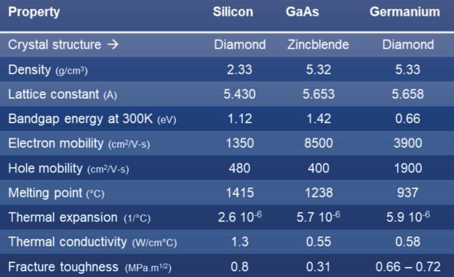
Germanium’s properties are very similar to GaAs
Due to the high level of maturity and low cost of silicon, many have dreamed of growing GaAs-based devices on this substrate.
However, despite 40 years of effort, little progress has been made. It is incredibly challenging to form high quality layers, due to substantial differences in both the lattice mismatch and the thermal expansion coefficient. Fortunately, with germanium it is a very different state of affairs: the thermal coefficients of expansion are very similar; and GaAs, as well as AlGaAs, can be lattice matched to germanium.
The default position within our industry is that when it comes to the manufacture of small-surface devices, if native substrates are available, they are employed. This only tends to be questioned when the issue is cost, with GaN LEDs offering a primary example. For this reason, there has not been a sufficiently large incentive to switch from GaAs substrates to germanium variants for the production of GaAs-based photonics. But this is set to change, now that the manufacture of VCSELs and microLEDs is transitioning to larger volumes.
VCSEL volumes
Around the turn to the century, sales of VCSELs started to take off, due to increased deployment in multi-mode optical fibre links serving datacentres. Thanks to the incredibly small dimensions of the VCSEL, a hundred thousand can come from a single 100 mm wafer. This means that the datacoms sector is not a large volume business for the VCSEL, and it is completely justifiable to produce this class of laser on 50 mm and 75 mm GaAs substrates.
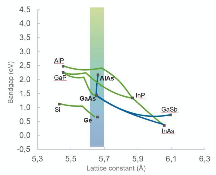
Germanium can be strain balanced with VCSEL GaAs/AlGaAs DBR structures
In 2017, the game changed when Apple launched a new generation of iPhone featuring VCSEL-based FaceID identification.
This innovation enabled makers of VCSELs to now enjoy far higher volumes, partly because they were finally tapping into a large consumer business. The facial recognition technology also drove up volumes, because rather than requiring a single VCSEL, smartphones needed a large-area VCSEL dot projector array. With only 4,000 VCSEL arrays fitting on a 100 mm wafer, a 100 mm line is no longer competitive. Yet another consideration is that the VCSEL arrays required a combination of a very low resistivity, to carry the current through the substrate; and a low density of dislocations, to ensure a reliable device and manufacturing yield – both of these are difficult requirements for a GaAs substrate.
There are only a few companies, IQE being one of them, that have the capability to grow the epistructures for the VCSEL on 150 mm GaAs substrates with sufficient yield. It is not easy to control the growth conditions so that the wavelength of the laser’s active region matches the reflectivity sweet spot of the distributed Bragg reflector (DBR) over a high proportion of the wafer. And even if this is accomplished, there are still homogeneity issues and device processing yield losses, along with significant bow, stemming from the GaAs/AlGaAs DBR structure.

At IQE’s epi fab in Cardiff, UK, engineers have spent several years investigating the growth of GaAs epilayers on germanium substrates produced by our facility at Umicore in Belgium. The merits of switching to germanium are not limited to those already described – namely the availability of substrates with no dislocations and a diameter of 200 mm or more, and the opportunity for strain-balancing – and extend to include the ease of recycling, competitive pricing and non-toxicity. So successful were the trials by IQE’s engineers, beginning in 2018, that last year the company started to commercialise its GaAs-on-germanium VCSELs.
Despite tremendous success at IQE, we are under no illusion that it will be easy to convince the VCSEL 3D industry of the cost and performance benefits of germanium. We know that we will have to work hard to support the transition all the way to consumer devices. History attests to plenty of examples of failed introductions of a disruptive technology. However, with the germanium VCSEL, the case is compelling, and we are in no doubt that this transition will take place.
For those that invest in the germanium VCSEL, the rewards reaped are not limited to the fortunes of facial recognition. That’s because the 3D sensing solutions developed for these high-end phones are already finding their ways in other markets. For example, there are many opportunities associated with robots that are spatially aware – they could serve in the automotive industry, as well as in a plethora of other devices in industry and consumer markets. Affirming this promise, according to the French market analyst Yole Développement, the 3D sensing industry is projected to grow by more than 50 percent over the next five years. And as volumes grow, only the best-performing, most cost-competitive solution will prevail.
Cost is also a primary concern for developers of microLED displays. This sector is still in its infancy, with consolidation yet to take place and a wide variety of microLED technologies still in development. At this stage, it is difficult to foresee which technologies will kick on and dominate direct-view and micro-displays.
But it is clear that InGaN and AlGaInP LEDs will both play their part. For the latter – and also to the resonant-cavity LED architectures – germanium wafers provide the same key benefits that they do to the VCSEL. What’s more, the opportunity to process 200 mm germanium-based wafers in 200 mm silicon lines could also play a major role in driving down the cost of microLED displays.
With so many merits, it is beyond question that the germanium substrate will play a bigger role in optoelectronic devices based on GaAs. Progress has been hampered by a fixation on homoepitaxy, but the floodgates are starting to open.
Record-breaking efficiencies strengthen the credentials of blue and green GaN-based VCSELs for serving in full-colour projectors for augmented-reality glasses
BY KENICHI TERAO, HITOSHI NAGAI, DAISUKE MORITA, SHINGO MASUI, TOMOYA YANAMOTO AND SHIN-ICHI NAGAHAMA FROM NICHIA CORPORATION
SERVING IN DISPLAYS, GaN-based laser diodes have had tremendous success. Their triumphs come from their many advantages over conventional lamps and LEDs, which include: a wide colour reproduction, a high power, a high luminance, a small spot size, and a high modulation speed. Today, watt-class blue and green GaN-based edge-emitting laser diodes are commercially available, primarily used in laser projectors and laser TVs.
At present, there is also increasing demand for a low-power laser, to be deployed in augmented-reality (AR) smart glasses. Such glasses may feature a retinal scanning display, with red, green and blue beams of light guided by a scanning MEMS mirror to project an image directly into the eye. To ensure eye safety, lasers that provide these beams of light must have a low optical output, making milliwatt-class lasers most suitable for this application.
One promising candidate for the light source of a retinal scanning display is the VCSEL. Compared to its edge-emitting cousin, it is better suited, thanks to a lower threshold current and a lower output power.
The lower threshold current, which benefits AR glasses by reducing power consumption and lengthening battery life, comes from a smaller emission volume. In a single transverse-mode VCSEL, the aperture diameter is typically 5 μm and the active layer thickness around 20 nm, resulting in an emission volume of 0.4 μm3. In comparison, typical single transverse-mode edge-emitting lasers have an emission volume that’s an order of magnitude higher (for a device with a cavity length of 200 μm, a 2 μm ridge width, and a 10 nm active layer thickness, the emission volume is 4 μm3).
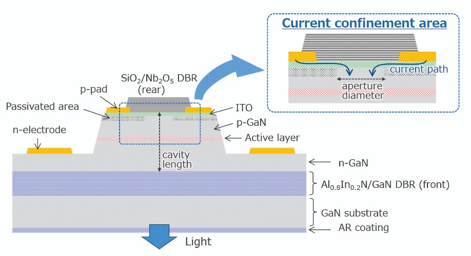
Figure 1. Nichia’s single-mode blue and green VCSEL chips pair a dielectric DBR with one based on nitrides.
From red to green and blue
Today, commercially available AlInGaP-based red VCSELs are well-established products; but their GaN-based blue and green variants lag behind, and are still under development. However, they are catching up, with efforts in the labs motivated by seeing them deployed in full-colour projectors for AR glasses.
At Nichia of Japan, we have a rich history in the development of the GaN-based VCSEL. Back in 2008 we reported the first demonstration of room-temperature CW lasing of violet GaN-based VCSELs by current injection. Building on this, by 2011 we had extended this to a blue version operating in the same manner, and a pulsed-driven green variant.
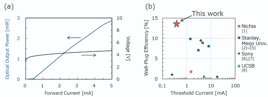
Figure 2. (a) Current-light (I-L) and current-voltage (I-V) characteristics of Nichia’s blue VCSEL under CW operation at 25 ºC. (b) Benchmarking the maximum wall-plug efficiency and the threshold current of blue VCSELs reported by several groups. [1] D. Kasahara et al. Appl. Phys. Express 4 072103 (2011) [2] M. Kuramoto et al. Appl. Phys. Lett. 112 111104 (2018) [3] M. Kuramoto et al. Appl. Phys. Express 11 112101 (2018) [4] M. Kuramoto et al. Appl. Phys. Lett. 115 041101 (2019) [5] M. Kuramoto et al. Appl. Phys. Express 13 082005 (2020) [6] T. Hamaguchi et al. Phys. Status Solidi A 213 1170 (2016) [7] T. Hamaguchi et al. Jpn. J. Appl. Phys. 58 SC0806 (2019) [8] J. A. Kearns et al. Optics express 27 23707 (2019).
Different DBRs
To avoid this problem, more recently we have turned to a design that pairs a dielectric top mirror with a bottom mirror based on an epitaxially grown Al0.8In0.2N/GaN DBR (see Figure 1). This is a similar approach to that taken by other groups, where researchers have investigated other combinations of nitride-based epitaxial DBRs, including AlGaN and GaN, and AlN and GaN. We prefer Al0.8In0.2N and GaN, because this lattice-matched pairing ensures defect-free, highly reflective mirrors.
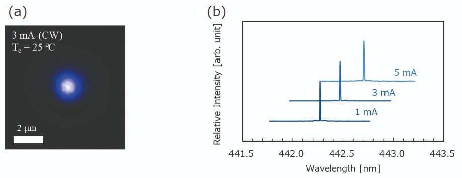
Figure 3. (a) Near-field patterns of Nichia’s blue VCSEL emitted from the AlInN/GaN DBR side under 3 mA CW operation at 25º C. (b) The emission spectra under 1 mA, 3 mA and 5 mA CW operation at 25º C. Note that the vertical axis has some offset for clarity. The red-shift of the peak wavelength is due to the refractive index change by self-heating.
During the past decade several papers have detailed studies of blue VCSELs with an AlInN/GaN DBR. Progress has been made, but until our recent breakthrough, the threshold current remained high, exceeding 1 mA. Another limitation that we have addressed is the lack of a green VCSEL with AlInN/GaN DBRs. Our latest generation of VCSELs overcome these shortcomings, thanks to optimised epitaxial layers and device structures. Our blue and green VCSELs provide milliwatt-class optical output power and recording-breaking wall-plug efficiencies.
Fabrication of our VCSELs began by taking 2-inch c-plane free-standing GaN substrates, loading them into an MOCVD reactor, and depositing an epitaxial stack that included an Al0.8In0.2N/GaN epitaxial DBR, n-type, active and p-type layers.
We defined a circular current-confinement region by passivating the p-GaN surface and depositing an indium tin oxide transparent electrode. One merit of this current-confinement structure is that it enhances the current density of the aperture area, and in turn reduces the threshold current required for laser oscillation – this can be obtained with a relatively small current of around 1 mA.
After forming the aperture, we added a p-pad, n-electrode, an Nb2O5 spacer layer and a SiO2/Nb2O5 dielectric DBR. This resulted in a 4.5λ cavity length, which is short enough for single longitudinal mode lasing. Note that for a 4.5λ cavity, longitudinal mode spacing is several tens of nanometres, which is wider than the gain spectrum width of the active layer and the stopband width of the AlInN/GaN epitaxial DBRs.
Final steps in our fabrication process involved: polishing the back surface of the GaN substrate; adding an anti-reflection coating; and dicing and mounting VCSEL chips on a heatsink, using a junction-down method in a TO-CAN package to suppress thermal resistance.
Highly efficient blues...
To evaluate our VCSELs’ optical output power, we have monitored the emission from the AlInN/GaN DBR side, because the reflectivity of the AlInN/GaN DBR is lower than that of the SiO2/Nb2O5 dielectric DBR. Measurements reveal that the threshold current for our single-mode blue VCSEL is 0.40 mA (Jth = 3.2 kA cm-2) and the threshold voltage is 3.75 V. Both these values are quite low for blue VCSELs. Optical output power is milliwatt-class (see Figure 2 (a)), and benchmarking shows that our VCSEL breaks new ground for wall-plug efficiency, 13.6 percent at 2.6 mA (see Figure 2 (b)).
These VCSELs show single-mode lasing. Near-field patterns reveal a fundamental transverse mode (LP0,1 mode), maintained up to at least 7 mA (see Figure 3(a)). This stable single transverse mode may be suitable for AR glass applications. Measurements of emission spectra under a range of forward currents show a single peak in the blue (see Figure 3(b)), indicating that our VCSEL lases with a single-transverse and a single-longitudinal mode.
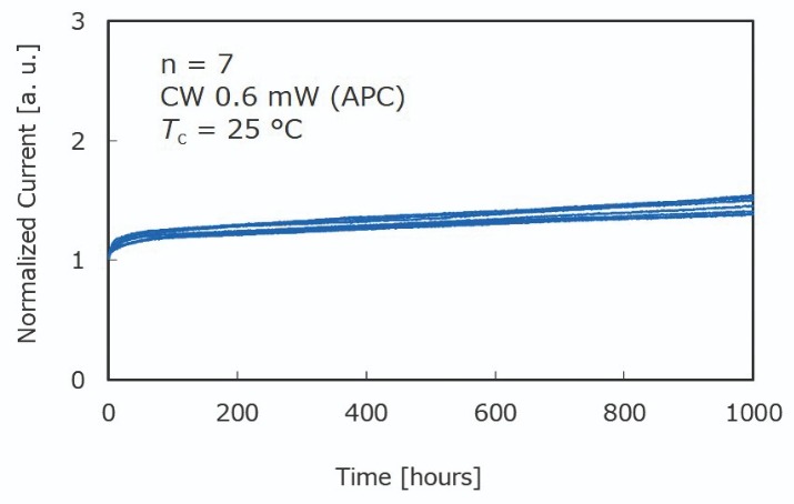
Figure 4. Lifetime test results of Nichia’s blue VCSEL chips under an automatic power control of 0.6 mW CW operation at a case temperature of 25 °C. Operating current is normalized by its initial value.
Another encouraging aspect of our work is the high yield. To oscillate a VCSEL, the resonant wavelength must be included within the part of the stopband of the DBR where reflectivity exceeds 99 percent. For an AlInN/GaN epitaxial DBR, stopband width is relatively narrow compared with that of a dielectric DBR, such as a SiO2/Nb2O5 DBR. Consequently, it is critical to control the thickness and composition of an AlInN/GaN DBR, to ensure that the stopband range is stable. By optimizing growth conditions for our AlInN/GaN epitaxial DBR and customizing our MOCVD system, we have excelled on this front, recording a high yield for our blue VCSEL chips.
One yardstick for evaluating yield is the threshold current. We have mapped this over a 2-inch wafer, considering only a region inside a circle with a 44 mm diameter (see Figure 5). This criterion reflects the instability in photolithographic patterning at the edge of the wafer. With this methodology, we calculate an effective area of over 90 percent at the average threshold current of 1 mA. This suggests that our fabrication process for making blue VCSELs with an AlInN/GaN DBR meets mass-production requirements.
... and milliwatt-class greens
Developing a green VCSEL is a more challenging than its blue cousin. One obstacle is the degradation of the quantum well at a higher indium content, and another is the decrease of optical gain in the long-wavelength region, associated with the quantum-confined Stark effect. As well as our earlier report of green VCSEL lasing, there are those from Sony and Xiamen University. All those efforts only realised a low optical power – ranging from several microwatts to several tens of microwatts – while the threshold voltage remained high. With the wall-plug efficiency is pegged back to below 0.1 percent, practical use of green VCSELs in commercial applications is unlikely.
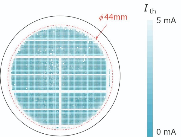
Figure 5. Threshold current mapping of a 2-inch wafer. Some blank lines correspond to test element group (TEG) areas, where a VCSEL chip was not fabricated.
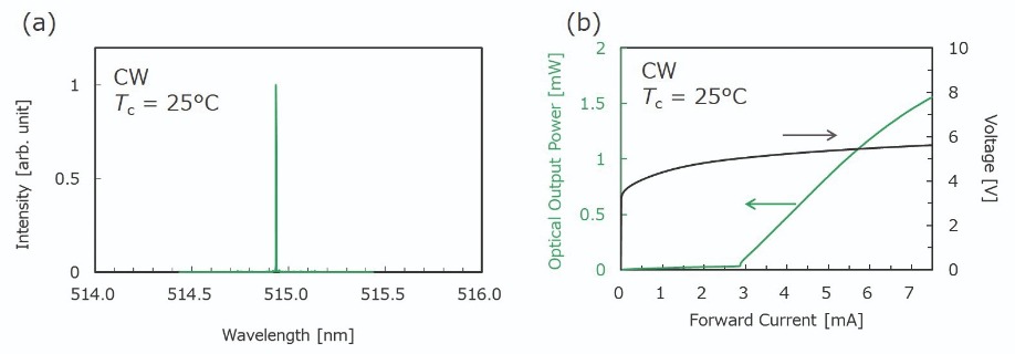
Figure 6. (a) The emission spectrum of Nichia’s green VCSEL under 4.8 mA CW operation at a case temperature of 25º C. (b) Current-light (I-L) and current-voltage (I-V) characteristics of Nichia’s green VCSEL under CW operation at 25º C.
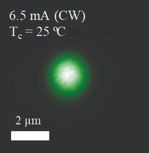
Figure 7. Near-field patterns of Nichia’s green VCSEL emitted from the AlInN/GaN DBR side under 6.5 mA CW operation at 25 ºC.
Germanium trumps GaAs as the best substrate for the VCSEL, thanks to improved lattice engineering that trims bow and warp
BY ANDREW JOHNSON FROM IQE
ONE OF OUR INDUSTRY’S GOLDEN RULES is that whenever possible, you should grow your device on a lattice matched native substrate. Following that advice, the best InP devices are produced on InP substrates, and the vast majority of GaAs-based devices have been manufactured on a GaAs foundation. To service these requirements, a large supply chain infrastructure has evolved over the past 30 years.
Most golden rules have exceptions, and in our industry they are found with GaN. Due to the absence of affordable large-area GaN substrates, producers of GaN-based LEDs manufacture these emitters on sapphire.
There’s now another exception to this rule of employing a native substrate, and in this case it will raise a few eyebrows – it’s the use of a foreign substrate for the GaAs-based VCSEL. Why is this appropriate? Well, due to increased demand for this class of laser for 3D sensing applications, there has been a shift in production from 75 mm to 150 mm GaAs substrates, with the introduction of the larger diameters exacerbating bow and warp to the extent that distortions typically exceed 200 μm. Such a significant bow and warp stems from the small lattice mismatch between the GaAs substrate and the AlGaAs constituents of the thick VCSEL DBR layers, which combine to create a net compressive strain in the epistack. Due to a total epilayer thickness that tends to exceed 10 μm, there is significant strain across the full epitaxial structure, causing distortions to the epiwafer.

Figure 1. Mapping 980 nm VCSEL epiwafers with a Flatscan Optical 3D Surface Profilometer reveals that switching the substrate from GaAs (shown on the right) to germanium (on the left) leads to far flatter wafers. For the VCSEL structure grown on GaAs, the wafer has a convex distortion, with a peak-to-valley distance of around 227 µm. In comparison, when the same epistack is grown on germanium, it produces a peak-to-valley variation of less than 25 µm. Note the difference in the vertical scales on the two graphs.
At IQE’s fab in Cardiff, UK, our engineers have tackled these issues by developing a process for growing 940 nm, GaAs-based VCSELs on germanium substrates. Our patented technology, known as IQGeVCSEL, overcomes many of the downsides of the conventional architecture, thanks to a lattice parameter that sits almost midway between those of GaAs and AlAs. By substituting germanium for GaAs, we virtually eliminate strain, the root cause of bow and warp.
Merits of the switch to germanium are not limited to minimising bow and warp. As germanium is mechanically more robust than GaAs, there are fewer wafer breakages during manufacture, and the wafers can be much thinner (note that 150 mm diameter germanium substrates for multi-junction solar cells are typically around 230 μm-thick, compared with a thickness of 670 μm for GaAs substrates of the same diameter that are used for making VCSELs). In addition, germanium wafers are readily available in diameters of 150 mm and 200 mm; they are dislocation free, so result in a higher VCSEL chip yield and better device reliability; and their use permits the growth of thicker DBR mirrors, used in longer-wavelength VCSELs that could serve in emerging markets. Yet another attribute of germanium is its extant market, with hundreds of thousands of large-diameter germanium wafers produced every year for makers of solar cells for space.
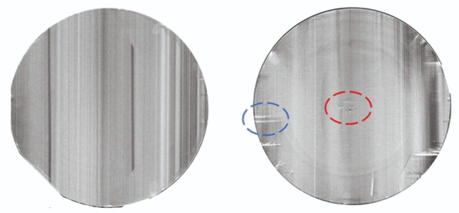
Figure 2. X-ray topography uncovers imperfections in the VCSEL structure grown on GaAs (right), not present in germanium (left). Blue and red rings highligh crystalline slip and bulk dislocations, respectively. There are annular features on the GaAs wafer, due to strain associated with doping striations. There is very heavy silicon doping in these substrates, incorporated to reduce bulk dislocation densities. The extended vertical lines, which are XRT measurement artefacts, are not associated with bulk or epitaxial material quality.
For both architectures, our engineers produced VCSEL epiwafers with the same structure and growth recipe on n-type 150 mm GaAs and germanium substrates. Germanium wafers were supplied by Umicore Electro-Optical Materials in Olen, Belgium, the leading global supplier of germanium wafers. The 940 nm and 980 nm VCSEL structures were produced on both types of substrate in the same epi-reactor, using the same growth recipe, and generally in consecutive growth runs. We adopted this approach to remove as much variability from the growths as possible, and enable a true like-for-like comparison of the structures.
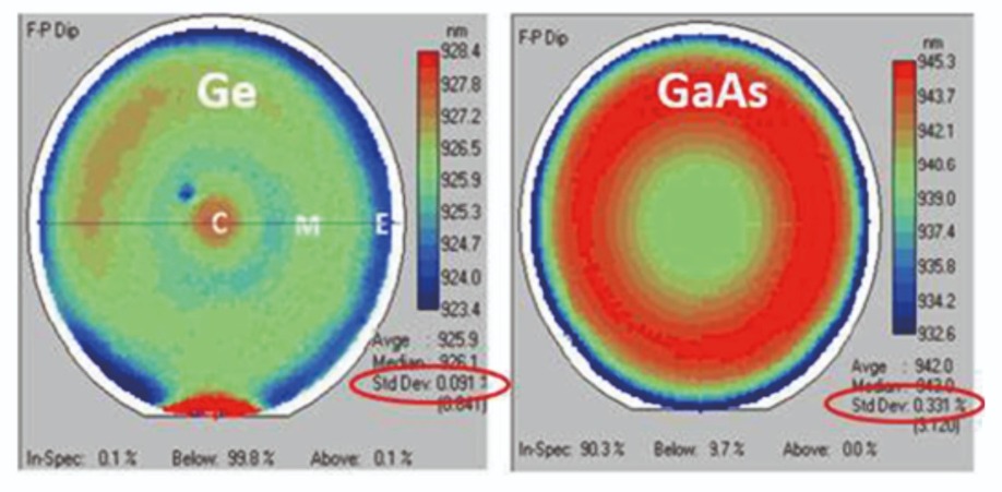
Figure 3. Wafer maps of the Fabry-Pérot dip parameter show that for the 940 nm VCSEL structure, the standard deviation for this figure of merit is more than three times lower when the substrate is germanium (left), rather than GaAs (right). Note that the standard deviation is ringed in red.
Following the growth of a range of VCSEL epiwafers, our team has scrutinized this material with a variety of techniques to evaluate wafers, including wafer bow, surfscan, X-ray diffraction, X-ray topography, photoluminescence and reflectivity. After this, we shipped our wafers to a fabrication partner at the Industrial Technology Research Institute (ITRI) in Taiwan, where VCSELs were produced from this material, allowing comparisons of device performance.
Confirmation by characterisation
So promising is the use of the germanium substrate that even the first growth of 980 nm VCSELs on this foundation demonstrated its inherent advantages. Wafer-bow measurements with a Flatscan Optical 3D Surface Profilometer, the 3D200, showed that VCSELs grown on GaAs have a total warp in excess of 225 μm, stemming from the residual compressive strain embedded within the epitaxial stack (see Figure 1). For the equivalent structure grown on germanium, a ‘saddle’ profile is observed, with a vertical distortion of the wafer of about 25 μm – that’s roughly an order of magnitude lower than that of the GaAs substrate.
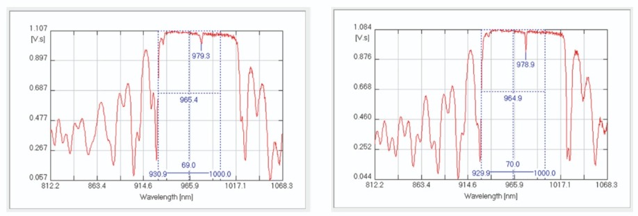
Figure 4. There is minimal difference in the VCSEL reflectivity curves for identical 980 nm structures grown on germanium (left) and GaAs (right) substrates.
Insights into the optical properties of the epiwafers have been provided by reflectivity maps. Profiles of the Fabry-Pérot dip parameter across the 940 nm VCSEL epiwafers are far more uniform when the underlying substrate is germanium (see Figure 3). Such a result shows that germanium has significant benefits, given that our team at IQE has devoted many years to optimising the MOCVD process on GaAs to take into account the inherent bow in GaAs epiwafers, and that the same epitaxial process has been used for growth on both types of substrate. One can expect further gains in uniformity on germanium substrates by refining the process for this foundation, so that it accounts for lower wafer distortion and a different temperature profile.
For the 980 nm VCSEL structures, we have compared spectral charts at the wafer centre (see Figure 4). In this case, spectra obtained for VCSELs grown on GaAs and germanium are to all intents and purposes identical. Usual reflectivity parameters – such as Fabry-Pérot dip, stop-band width and stop-band height – are the same, within experimental error. These findings offer additional confirmation of the promise of replacing GaAs with germanium when producing VCSELs.
Proven performance
The superiorities unveiled in characterisation are of little benefit unless they go hand-in-hand with improved performance. To see if that is the case, our partner at ITRI has taken our epiwafers and fabricated 940 nm VCSELs with 8 μm apertures. Note that the purpose of this investigation is not to demonstrate state of the art VCSEL performance, but make a direct comparison between the two types of VCSEL, while minimising the number of variables. Plots have been made of light-current-voltage characteristics, along with power and power-conversion-efficiency as a function of drive current (see Figure 5). These graphs indicate that VCSELs produced on a germanium substrate outperform those grown on GaAs.
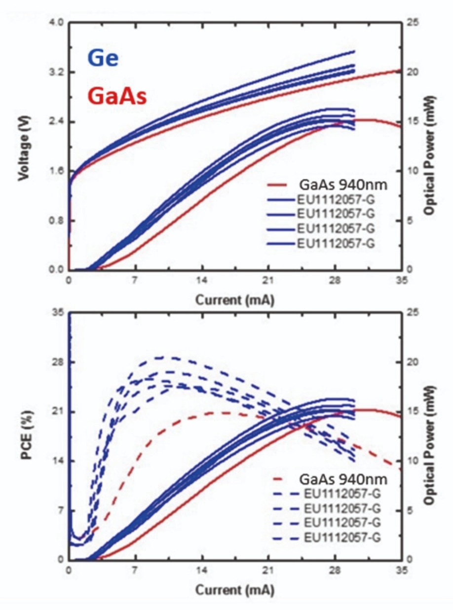
Figure 5. Light-current-power (L-I-V) and power-current curves for 940 nm VCSELs with an 8 µm aperture size, grown on germanium (blue) and GaAs (red) substrates. In general, the performance of VCSELs grown on germanium outperforms that for equivalent devices grown on GaAs.
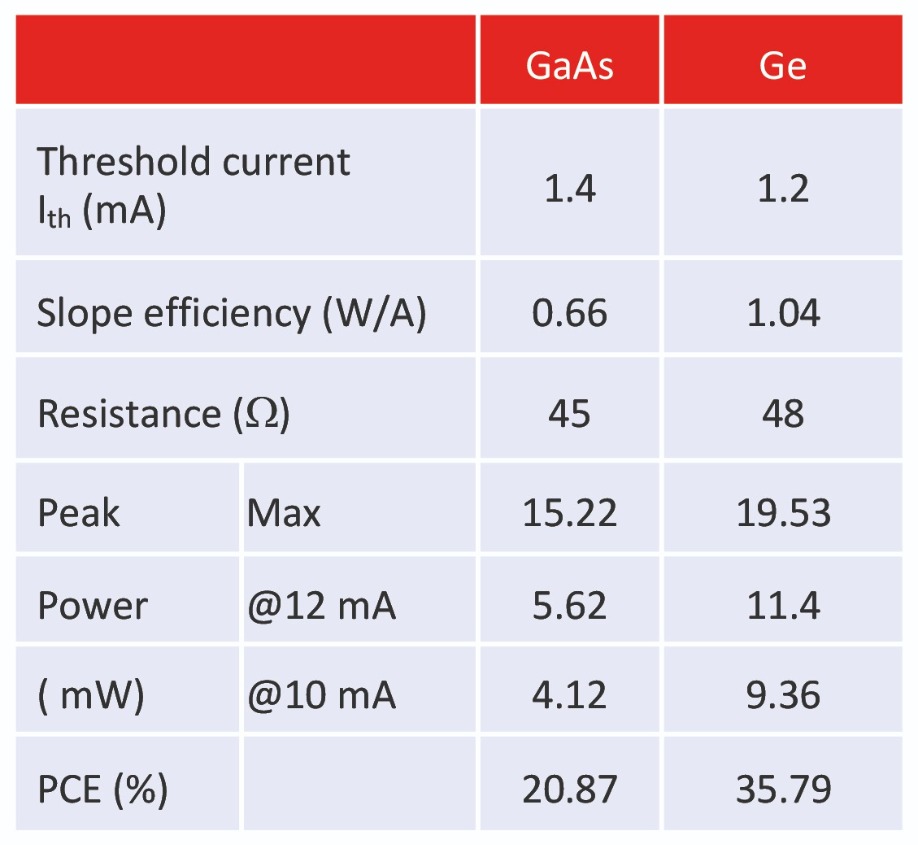
Table 1. According to a summary of standard VCSEL characteristics realised on the best-performing 940 nm devices grown on GaAs and germanium substrates, switching to a non-native substrate improves some characteristics, while making little impact on others.
Optimised grinding yields, flat and smooth SiC substrates in a matter of minutes
BY DIEGO CALVO RUIZ FROM MEISTER ABRASIVES
GROWING DEMAND for power devices with higher power ratings, faster switching frequencies and elevated operating temperatures is driving an increase in the adoption of SiC. Compared with the incumbent technology, silicon, this wide bandgap semiconductor provides a breakdown field strength that is ten times higher and a thermal conductivity three times higher – attributes that enable SiC’s use in incredibly efficient switching at high voltages and frequencies.
To cater for the strong, ramping demand for SiC devices, manufacturers of these devices are searching for ways to increase the capacity of their manufacturing lines. In parallel, they are re-evaluating their materials and processes, in search of new ways to streamline production. One essential ingredient for mass production of SiC-based power devices is a native substrate with a high-quality surface finish. When treating the surface of this substrate, opportunities for increasing productivity include reducing both the number and the duration of grinding and polishing steps.
The production of state-of-the-art SiC substrate requires pre-processing steps, involving several cycles of lapping or mechanical diamond polishing, followed by chemical mechanical polishing (CMP). These are processes that entail many steps and high machining costs, due to slow material removal rates. To cut consumable costs, there is a growing preference to grind 150 mm and 200 mm substrates with consolidated diamond abrasive technology, rather than lapping.
Surface matters
Meister Abrasives, headquartered in Andelfingen, Switzerland, has developed ultra-fine grinding technologies that take into account the well-known hardness and strength of monocrystalline and polycrystalline SiC. On 100 mm, 150 mm and even 200 mm SiC, Meister’s approach ensures a sub-nanometre average surface roughness (Ra), along with a total thickness variation (TTV) in the lower single digit range.
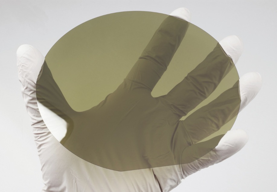
Figure 1. A SiC substrate, produced with a Meister Abrasives SiC Ultra Fine 6 grinding wheel.
At the heart of Meister Abrasives’ novel grinding technology, capable of producing SiC surfaces with unparalleled quality, is the proprietary bond-grit formulation. It features bonding structures, which are abrasive grains bound in a vitrified matrix system. With this approach, the same number of grains are active in the work zone. When material removal takes place on the substrate, new, sharp diamond grains are introduced by the matrix system.
Meister Abrasive’s bond-grit formulation offers several advantages over competing technologies. As the diamonds employed in the wheels are specifically selected to the grinding process applications, the benefits include enhanced cutting behaviour, excellent self-dressing behaviour and improved cooling. By developing new bond-matrixes, specifically tailored for each grit size, Meister offers a single bond for each wheel technology, leading to reaching a longer lifetime and lower grinding forces.
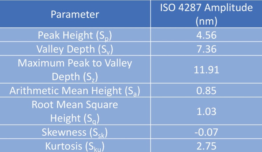
Table I. Area roughness parameter measurements of Figure 1 obtained with Filmetrics Profilm3D via WLI (White Light Interferometry).
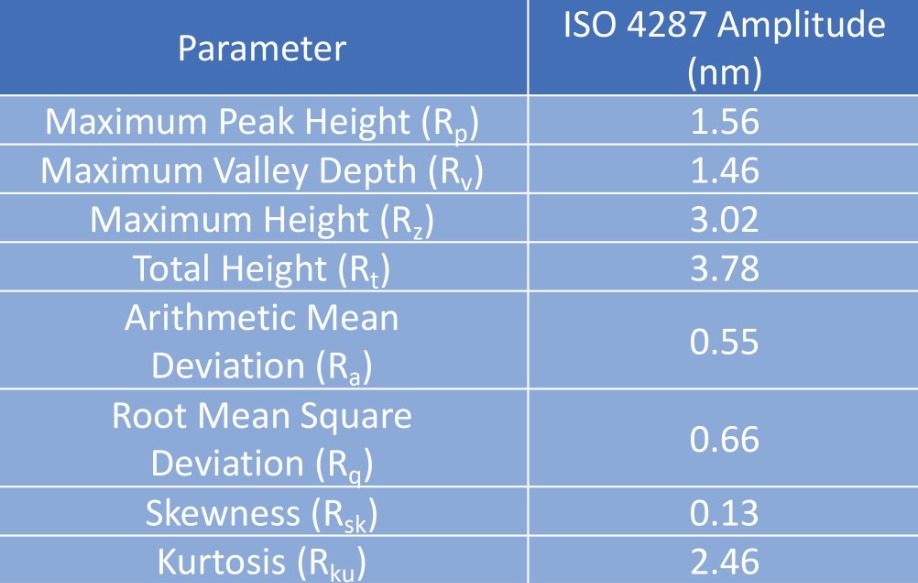
Table 2. Line roughness parameter measurements of Figure 1 obtained with Filmetrics Profilm3D via WLI.
Grinding versus lapping or polishing
Similar to lapping and polishing, grinding requires a grinding wheel backed by a rigid plate. When the wheel is in use, abrasive grains cut into the material being ground, removing unwanted surface material.
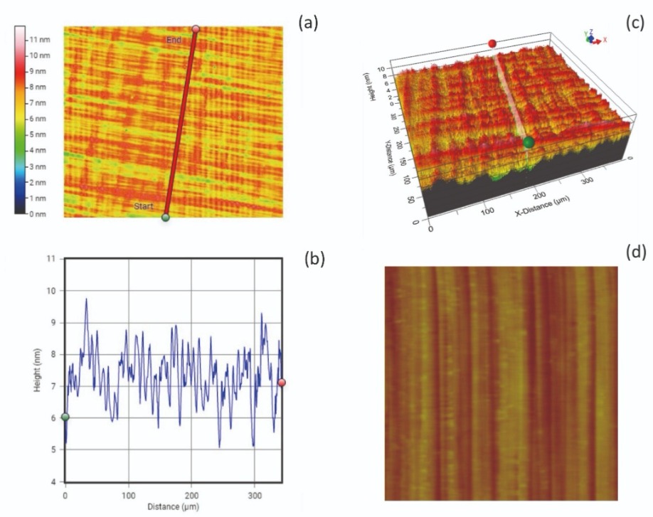
Figure 2. Selected region (400 µm by 350 µm) from Meister Ultra Fine ground SiC wafer: (a) contour topographic analysis of top view; (b) line profile of diagonal represented in (a); (c), 3D view of identical area; and (d), atomic force microscopy scan of a 5 µm by 5 µm area (note the Z-scale is 3.16 nm).
For normal grinding, it is essential to dress the wheel with a dressing tool. However, the number of dressing cycles is reduced with Meister’s open vitrified structures. Thanks to this, Meister Abrasive’s precision-engineered structured abrasives are cost-cutting and process time-saving solutions. Designed to work with any aqueous coolants, these abrasives reduce clean-up and waste disposal issues associated with abrasive slurries. Another important attribute is the absence of metal contaminations from the lapping plate to the substrate.
Following grinding industry standards, Meister Abrasives recommends a two-step approach to process substrates, with coarse grinding (usually called Z1) adopted prior to ultra-fine grinding (named Z2). For coarse grinding, roughness requirements are less critical, but industry prefers minimum wear: a factor that is especially relevant when a large amount of material needs to be removed prior to polishing. Using a tailored grit size and bond, Meister’s wheel specifications are optimised to target any kind of starting surface condition. This approach facilitates the processing of wire-saw, laser-sliced, lapped or etched surfaces off the substrates to the required thickness prior to the finishing step.
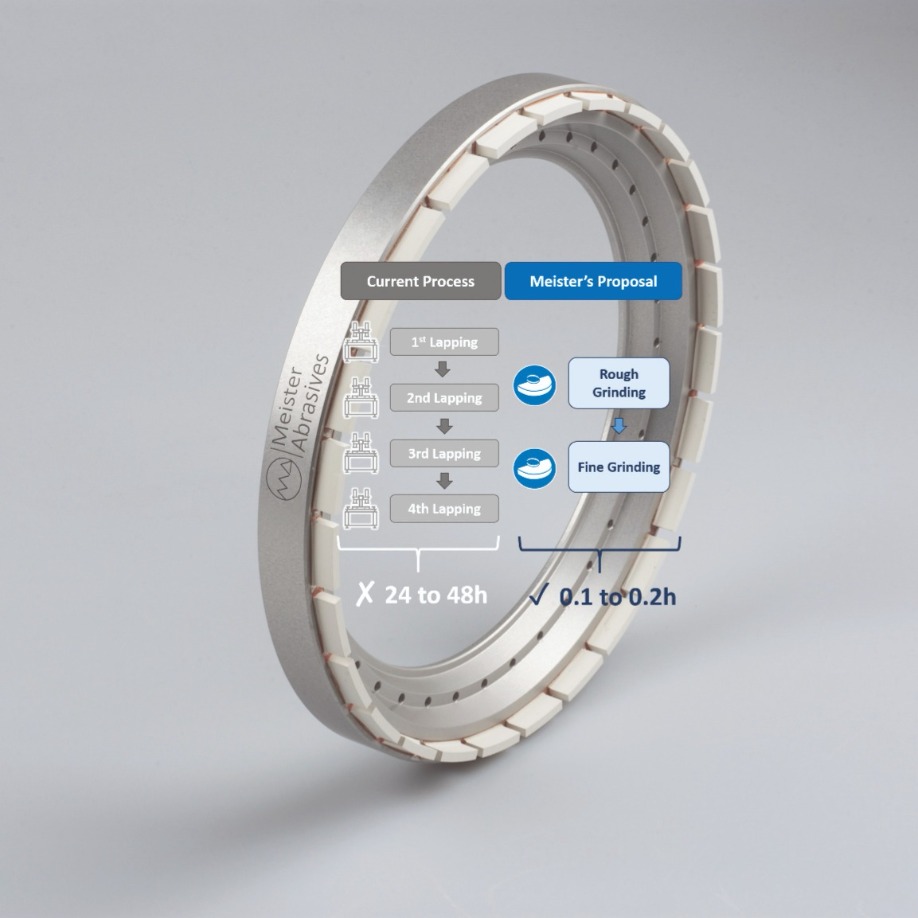
Figure 3. Comparison of the standard lapping processes versus Meister coarse and ultra-fine grinding technologies.
Upgraded vitrified bonds
Thanks to Meister Abrasive’s in-house development and production centre in Switzerland, for more than 70 years the company has been producing all the bonds that it uses, giving complete process control and the opportunity to provide customer-engineered solutions. A major technological advance has been the introduction of Meister’s vitrified superabrasives (CBN/diamond) tools in the early 1980s. Key to the success of this bond system is the outstanding abrasive properties of the largely porous structures, high stock-removal volumes and good wear properties.
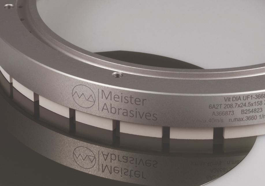
Figure 4. Representative ultra-fine wheel with a porous structure. This novel material, exhibiting a porosity that can be seen by the naked eye, maintains enough bonding to grind SiC.
Vitrified bonds tend to contain the following cations: Si4+, Al3+, Fe3+, Ti4+, Ca2+, Mg2+, K+ and Na+. Less common is Li+. All of these bond systems are free from lead, an advantage for both health and application reasons. The bond system’s chemical and physical properties are determined ultimately by the combination of raw materials and grit sizes, along with the firing cycle – that is, the vitrification process.
The microstructure is governed by the relative proportion of: abrasive grits, and their specific mix of type and size; the bond content; and the residual pore volume. Getting this just right is an essential precondition for an efficient tool.

Figure 5. Meister’s production facilities in Andelfingen, Zürich (Switzerland).
Red, green and blue edge-emitting lasers with milliwatt output powers and exceptional efficiency are lining up for augmented-reality applications
BY MARCO ROSSETTI, MARCO MALINVERNI AND ANTONINO CASTIGLIA FROM EXALOS
THERE ARE PLENTY REASONS why you might be looking forward to the augmented reality (AR) revolution. Maybe you want to get your hands on this technology; or maybe you are looking forward to the hike it will deliver in the sales of light-emitting devices.
At this stage, however, it’s best to temper your excitement. That’s because you’ll need to wait a few years while a number of technological hurdles are overcome that will allow wearable displays and smartglasses to be acceptable for consumer adoption. Progress is being made, though: there is the emergence of red, green and blue laser diodes, in the form of miniaturized optical engines, that are capable of bridging some important gaps related to display design and performance.
Playing a key role in this endeavour is our team at Exalos, a well-established maker of semiconductor light sources based in Switzerland. Recently, we have developed visible laser diodes that break new ground for low drive currents and minimal power consumption. These strengths, in demand for next-generation AR displays, give our lasers the credentials to compete in this sector with VCSELs, which are undoubtedly promising but less mature.
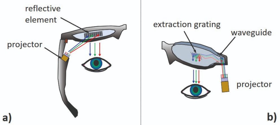
Figure 1. (a) AR glasses can be based on free-space projection and a reflective combiner. (b) A common alternative AR projection scheme, using integrated waveguides and extraction gratings.
Fortunately, it is possible to address all the key requirements for head-mounted displays with laser-beam-scanning display architectures, which are gaining traction. Several big names are active in this field, including Microsoft, Intel, Bosch, and Google/North. These high-tech companies lead the way in using laser diodes in AR hardware, and other firms are expected to follow.
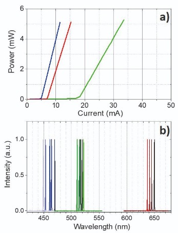
Figure 2. (a) Output power versus drive current for very-low-threshold red, green and blue laser diodes realized by Exalos (curves are colour coded); (b) set of spectra from multiple laser diodes in the three primary colour ranges. Each lasing line is relative to a different laser diode: Exalos targets specific wavelengths by changing the active region composition.
Waveguides versus projection
See-through AR smartglasses can be split into two main categories. One combines a waveguide structure, employing total internal reflection to couple light into a lens, with an extraction grating that delivers images to the user’s eye. The common alternative involves free-space projection and reflection off the lens. As we’re about to see, both have pros and cons (see Figure 1).
One of the merits of the waveguide approach is that it can be designed to deliver a good level of visual comfort, due to large eye boxes – thanks to them, when the pupil moves around, there is no difficulty in seeing the image. However, the use of waveguides creates a number of problems related to image quality and display efficiency. With this architecture, there are issues that result in a less than satisfactory AR experience, arising from a combination of chromatic dispersion and artefacts related to the waveguide structure and extraction gratings.
Another downside of waveguides is that they can produce extremely lossy coupling of light to the eye, with efficiencies of 1 percent or less not uncommon. Due to the large optical loss of the system, light sources have to compensate by providing an optical power per colour ranging from several tens of mW to 100 mW. Such a high output drives up power consumption and leads to a larger projector size, needed to handle heat dissipation. This state of affairs is hampering the fulfilment of the consumer’s wish for the development of slim glasses weighing no more than 70 grams.
The strengths of free-space reflective displays are a simpler optical design, the generation of higher quality images, and exceptional efficiency in relaying light from the projector to the user’s retina; thanks to this, they require a far lower power from the light sources. Despite a smaller eye box, the simplified design and the strongly reduced power consumption make this option an excellent candidate for consumer-type AR-glasses. In this case, the required optical power from each laser diode is only a fraction of a milliwatt, rising to a few milliwatts when accounting for the optical loss of the projector unit and the reflective element.
Is it possible to fulfil these requirements with red, green and blue laser diodes? Well, there’s hope, thanks to a major evolution over the last two decades in blue and, in particular, green laser diodes based on GaN and its related alloys. During that time there have been fundamental technological breakthroughs in efficient p-type doping and the realisation of high-quality active regions emitting in the green. In addition, much effort has been directed at developing reliable devices that deliver ever-higher output powers for industrial and large-area display applications. However, low-power regimes with reduced power consumption remain largely unexplored. This explains why commercially available laser diodes are yet to meet the demanding requirements for free-space AR smartglasses.
Over the last few years much work has been directed at closing this gap by developing visible VCSELs. Promising results have come from both red VCSELs, based on AlGaInP, and blue and green cousins formed from the AlInGaN material system. However, these devices are at the proof-of-concept stage, with some major challenges holding back commercialization. The manufacturing process is complex, and there are technical issues related to the production of good multi-layer mirrors and efficient active regions. So far, these challenges are imparting a heavy toll on production yield and performance homogeneity.
Tiny threshold currents
We are championing an alternative to the VCSEL through our development of a range of edge-emitting lasers with very low threshold currents. These devices, manufactured with conventional semiconductor wafer processing tools, address the performance gap by delivering a few milliwatts of optical power at a fraction of the drive current required for the typical laser diode of today. Our low-power blue and red laser diodes have threshold currents near 5 mA and operate below 10 mA; and our green variants start lasing near 15 mA, and run between 20 mA and 30 mA (see Figure 2). Operating voltages at threshold are 2.3 V, 3.7 V and 5.5 V for our red, blue and green laser diodes, respectively, and corresponding figures for electrical power consumption at an optical output power of 3 mW are roughly 25 mW, 35 mW and 160 mW.
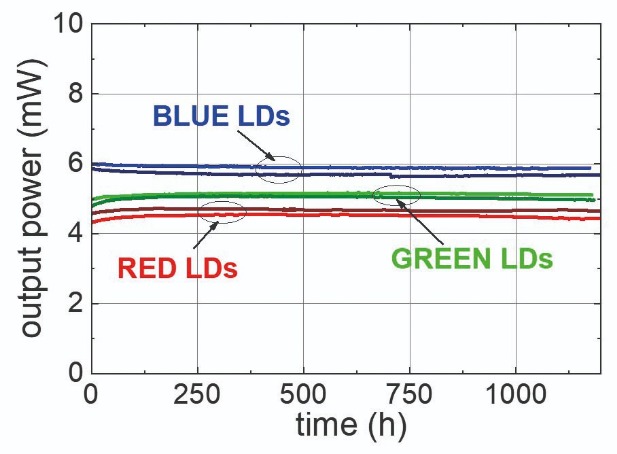
Figure 3. Lifetime curves for red, green and blue laser diodes under continuous-wave injection at a constant current and a test temperature of 25 °C.
As well as offering excellent performance, our new laser diodes provide great stability and long-term reliability. Lifetime curves, acquired under constant-current and continuous-wave operation, reveal that for more than 1,000 hours of operation at an output power near 5 mW, there is little or no power drop, indicating that these devices have much promise for deployment in consumer display applications (see Figure 3).
For those that are not familiar with III-nitride compounds, this lifetime for blue and green laser diodes might appear a routine result – but it is not, it is actually a major achievement. Our success is hard won, building on the breakthroughs we have made with our 405 nm SLEDs, which have a projected lifetime of about 5,000 hours.
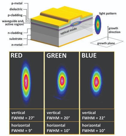
Figure 4. (Top) With ridge-waveguide laser diodes, the optical mode shape at the output facet governs the light beam pattern in the far-field. (Bottom) Light patterns of Exalos red, green and blue laser diodes detected with a CCD camera in the far-field. Images include the full-width at half-maximum (FWHM) of the angular distribution for the light intensity along the two primary directions.
A well-known issue for GaN laser diodes is a high level of defects, which degrade performance. Like many of our peers, we produce our devices on high-quality free-standing GaN substrates with a low dislocation density, a foundation that helps us to avoid crystal imperfections, particularly in InGaN-based quantum wells.
Another challenge associated with the production of III-nitride laser diodes is the realisation of p-doping. Our approach involves introducing magnesium atoms at carefully controlled dopant levels. We take care to avoid too high a magnesium level, as this could increase optical loss in the chip, and could eventually generate clusters and defects if crystal densities exceed a few 1019 cm-3. Note that it is crucial to not head too far in the other direction – if magnesium concentrations are too low, series resistance climbs alongside the device’s operation voltage, impairing device reliability.
In addition to considerations related to crystal growth, all makers of ridge-waveguide lasers need to ensure that the dielectric mirrors have very low absorption and scattering losses, and that the device has an appropriate package. It is imperative to have an inert package atmosphere that is free of contaminants, as this prevents degradation of the output mirror by photo-induced deposition processes that can take place during operation.
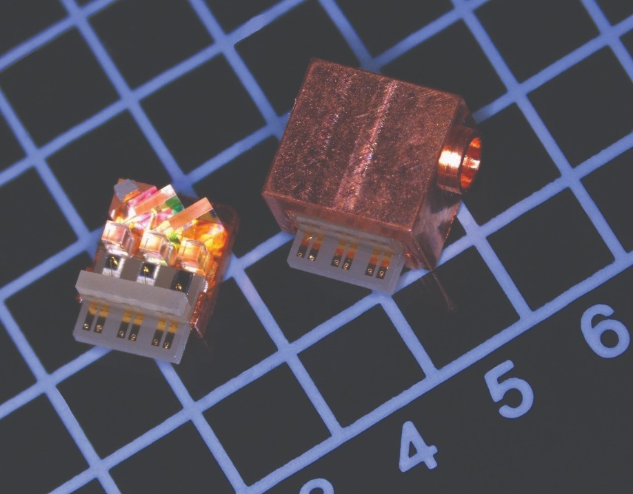
Figure 5. A compact integration layout for red, green and blue lasers used to generate a collinear, collimated beam. The underlying grid unit has a dimension of 2.9 mm.
One promising feature of the low-power laser diodes developed by our team is that all three colours produce a similar single-lateral-mode output pattern. This lack of variation significantly simplifies the integration of red, green and blue lasers with common collimation optics. Emission from the cleaved facets of our edge-emitting lasers has the typical elliptic shape, with a divergence that depends on the optical confinement of light in the chip.
With edge-emitting lasers, an important role is played by the two-dimensional refractive index architecture, defined over a cross-section of the ridge-waveguide structure. Along the epitaxial growth direction, angular beam divergence is determined by the thickness and composition of the core and cladding layers that provide waveguiding. For the direction parallel to the growth surface, divergence depends on the ridge-waveguide width, the etch depth and the refractive index of the dielectric layer that provides electrical insulation on each side of the ridge.
Careful optimisation of these parameters enables a great deal of control over the shape of the light emission. With this approach, we have realised extremely similar light patterns for red, green and blue laser diodes, despite their different semiconductor technologies. For all three colours, the typical slow-axis divergence, defined in terms of the full-width at half-maximum, is of the order of 9-10 °; fast-axis angular divergence is 20 ° for the green, 22 ° for the blue, and 24 ° for the red (see Figure 4).
For the red edge-emitter, which has a slightly larger divergence along the growth direction, the conventional core/cladding geometry is derived from that used previously for SLED epitaxial structures. We expect that with further optimization in future designs, we can adjust the optical confinement so that the red fast-axis divergence is even closer to that of the green and blue equivalents.
Our laser diodes set new standards for providing a few milliwatts of optical power at a very low power consumption, and they pave the way for efficient, compact pico-projectors for AR technologies. In these systems, the red, green and blue sources have to be integrated with micro-optics to generate a collinear, collimated white-light beam for the MEMS scanner.
We have significant expertise in this area, as we can draw on experience in producing tuneable lasers and spectrally-combined SLED sources, which make use of highly automated robotic assembly processes to position optical filters and lenses with sub-micron accuracy. We are currently prototyping ultra-compact light engines based on red, green and blue lasers that have a volume of about 50 mm3 (see Figure 5), to enable the next generation of AR smartglasses.
At this year’s Digital Optical Technologies conference, held in June, we presented a module 4.4 mm in length, 4.15 mm wide, and 2.9 mm high. With a perfect blend of semiconductor and packaging technologies at hand, we have a bright future ahead of us.
Exalos expertise
Exalos has more than two decades of experience in advanced light sources based on compound semiconductor devices. Expertise includes material systems, such as those based on InP, GaAs and GaN. Since 2003, the company has shipped more than 500,000 devices with light emission spanning the UV-visible (405 nm) to the near-infrared (1700 nm) (see Figure below).
The key enabling technologies for this are superluminescent diodes (SLEDs) and external-cavity lasers, which are used extensively in medical and industrial imaging, navigation, optical sensing, metrology and scientific applications. Exalos has built up a large customer base in different application areas, has a proven track record of commercial success and a strong spirit of innovation. With this foundation, it was a next natural step for the company to turn its attention to higher-volume consumer applications.
Since 2018, Exalos has been particularly active in the field of AR, providing red, green and blue SLED sources and customized solutions to multiple players. These devices combine the spatial coherence and beam-like output of laser diodes with the large spectral bandwidth and low temporal coherence of LEDs. Armed with these attributes, SLEDs provide a nearly speckle- and artefact-free projection – these are highly desirable features for AR solutions that include the use of waveguides.
Exalos claims that, to date, it is the only company on the market able to deliver red, green and blue SLEDs. These devices have a lot in common with edge-emitting laser diodes. For this reason, Exalos says that it finds itself in an excellent position to take the further step of delivering lasers with low power consumption for free-space AR-combiners. This is a perfect match to its innovation strategy, allowing the company to leverage its existing compound semiconductor know-how.
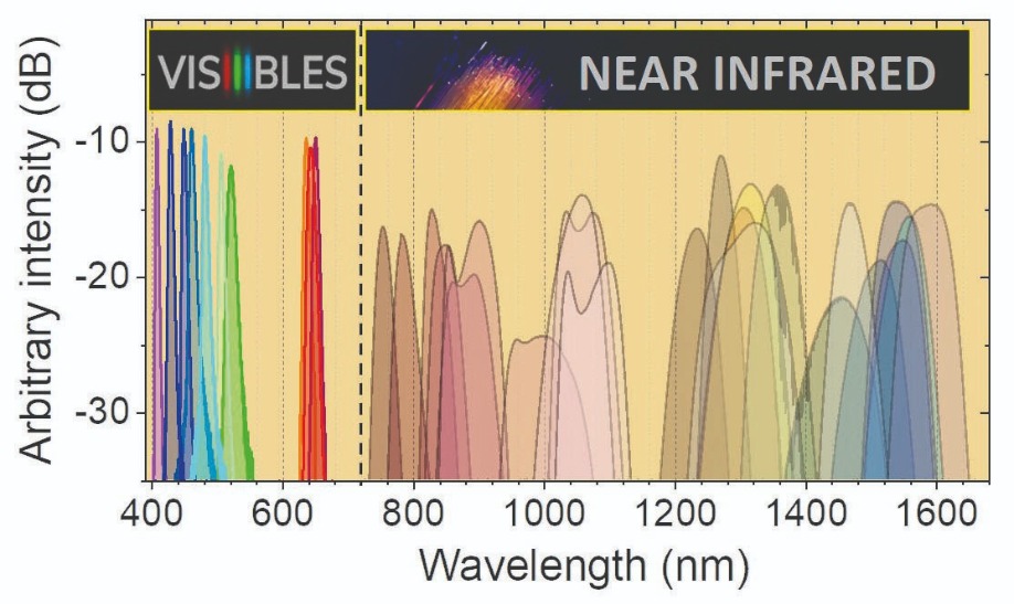
Spectral plots of visible and infrared SLEDs provided by Exalos.
Further Reading
SiC membrane supports record-breaking modulation rates for InP lasers
BY SUGURU YAMAOKA, NIKOLAOS-PANTELEIMON DIAMANTOPOULOS, HIDETAKA NISHI, TAKAAKI KAKITSUKA AND SHINJI MATSUO FROM NTT AND FUMIO KOYAMA FROM TOKYO INSTITUTE OF TECHNOLOGY
GLOBAL DATA TRAFFIC is continuing on a strong upward trajectory, due to growth in various internet services, such as smartphones, cloud services, and the Internet of Things. This growth comes with a cost, the substantial increase in power consumption at data centres. To try and address this, and reduce the associated carbon footprint, there is much interest in trimming the power consumption of the optical transmitters and increasing their modulation speed.
Directly modulated lasers (DMLs) are attractive contenders for optical transmitters, combining a small footprint with a low cost and a frugal power consumption. These strengths stem from the simple data transmission principle of the DML, with modulation of the injection current encoding data on the laser’s output power. In the form of a VCSEL, DMLs are widely used in short-reach optical interconnects. However, they are up against a barrier – for the last 30 years they have been limited to a 3 dB modulation bandwidth of around 30 GHz, which has prevented them from realising the desirable symbol rate of 100 GBaud for beyond 400 Gbit-Ethernet (400GbE) applications.
For such applications, those that build today’s networks combine CW lasers with external modulators, such as electro-absorption modulators and Mach–Zehnder modulators. Both these pairings can already provide 100 GBaud modulation.
However, these solutions have a larger footprint than the DML, consume more power, and are more expensive, due to the requirement for more chips. With all these drawbacks, much research is directed at expanding the bandwidth of the DML.
When the injection current is varied in a DML, it induces a dynamical carrier-photon interaction, leading to a relaxation oscillation. The frequency of this oscillation governs the intrinsic modulation speed. Options for increasing this oscillation frequency, and thus the modulation speed, are to increase the optical confinement factor, the differential gain, the current density, and the internal quantum efficiency. Since the 1990s, many researchers have focused on differential gain, seeking improvements in the active regions in the O- and C-band that contain strained multi-quantum wells. However, the relaxation oscillation frequency has plateaued at around 20 GHz.
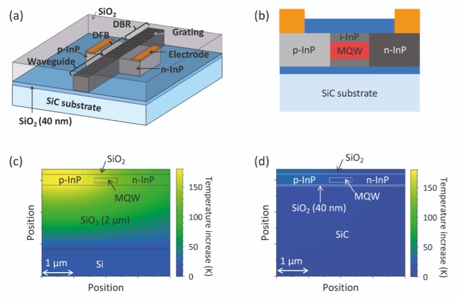
Figure 1. (a) NTT’s membrane distributed-reflector laser on 40 nm-thick SiO2-on-SiC. (b) Cross-section of the DFB section. (c) Calculated temperature increase for the laser on 2 µm-thick SiO2-on-silicon. (d) Calculated temperature increase for the laser on 40 nm-thick SiO2-on-SiC. Calculations assume a 50 µm by 0.7 µm by 0.15 µm multi-quantum-well region and a 100 mW heat source in the p-InP region. The InP slab thickness is 340 nm.
For a further gain in the 3 dB modulation bandwidth, it is crucial to increase the intrinsic relaxation oscillation frequency. One promising way to do this is to boost the optical confinement factor.
At NTT, Japan, we have adopted this approach, beginning with the fabrication of membrane lasers on 2 μm-thick SiO2-on-silicon. This combination ensures a high degree of optical confinement, with thin high-refractive-index multi-quantum wells sandwiched between low-refractive-index SiO2 and air. Thanks to a high degree of optical confinement, the threshold carrier density is low, leading to a reduction in power consumption.
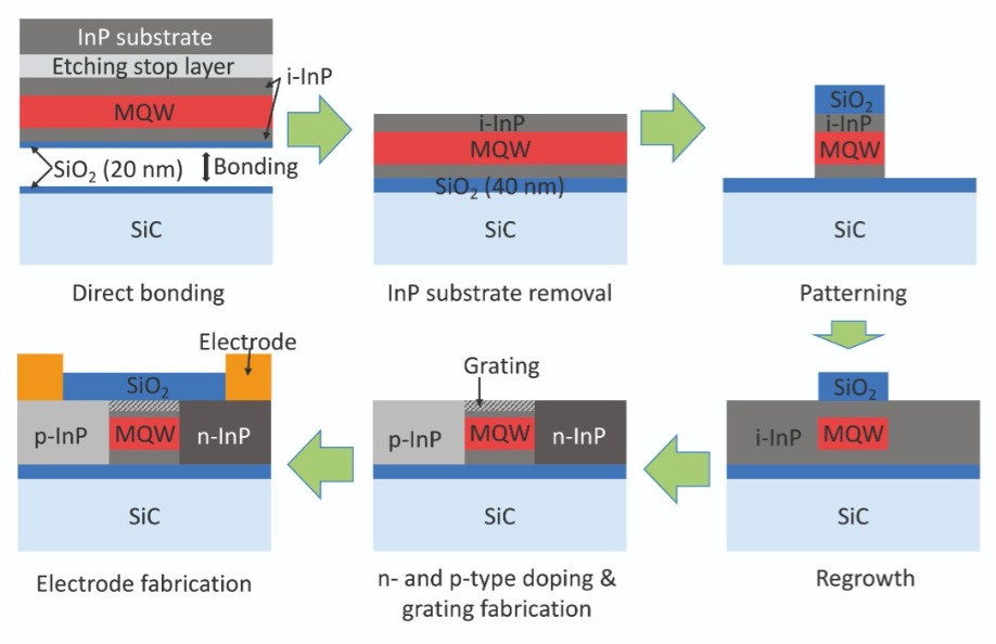
Figure 2. Fabrication procedure for membrane lasers on SiC.
While this result is promising, with the laser exhibiting a high modulation efficiency, it did not lead to any increase in the intrinsic relaxation oscillation frequency – this still had a value of around 20 GHz. The thick, low-thermal-conductivity layer of SiO2 held back the laser, with the temperature of this device increasing relatively quickly with bias current, and hampering differential gain. Note that it would be folly to decrease the thickness of the SiO2 layer to address this issue, as that would lead to more light entering the silicon substrate, and ultimately reduce optical confinement.
Introducing the SiC substrate
To prevent overheating of the laser, we have modified our architecture, moving to a high-thermal-conductivity material. When selecting this successor, we considered whether it would provide a low enough refractive index to realize high optical confinement in the active region, and whether it would be transparent in the O- and C-band. Attractive candidates for meeting these requirements are wide-bandgap semiconductors, such as diamond, GaN, AlN, and SiC.
From this class of material we selected SiC. Influencing our decision is the commercialisation of single-crystal SiC substrates by various companies. The growing market for high-power electronics has led to the availability of larger SiC wafers, up to 150 mm in diameter. This material has a very high thermal conductivity, with a value of 490 W m-1 K-1, compared with just 1 W m-1 K-1 for SiO2. The refractive index for SiC of around 2.6 is also suitable, ensuring comparable optical confinement to that on SiO2-on-silicon.
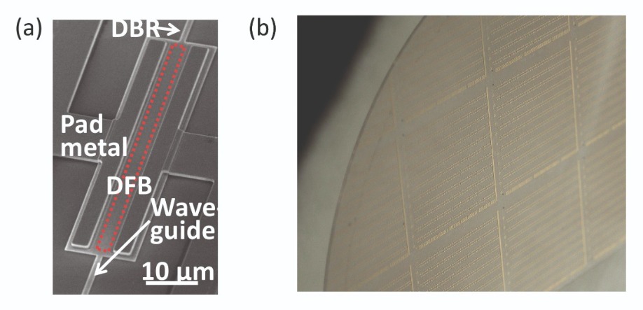
Figure 3. (a) Top-down view of NTT’s fabricated distributed-reflector laser with a 50 µm-long active region on SiC. (b) Image of numerous membrane lasers fabricated on a transparent SiC wafer.
Our key process to realising our membrane laser on a SiC substrate (see Figures 1(a) and 1(b)) is the application of a low-damage oxygen-plasma-assisted direct-bonding technique with an ultrathin SiO2 layer. Use of a 40 nm-thick SiO2 layer increases heat dissipation in the active region and reduces plasma-induced damage to the multi-quantum wells.
According to our calculations, by switching from our previous design with the laser on a 2 μm-thick SiO2-on-silicon foundation to our new architecture – that is, a 40-nm-thick SiO2 layer on SiC – slashes the increase in temperature by 88 percent (see Figures 1(c) and 1(d)). Thanks to this, we can increase bias current without degrading differential gain, and ultimately increase the relaxation oscillation frequency.
The laser that we have fabricated has three sections: a distributed feedback (DFB) section, a rear distributed Bragg reflector (DBR) mirror, and a waveguide. Incorporating a distributed reflector structure enables single-mode lasing, using the DBR to select one side mode of the DFB grating. By altering the reflectivity at the facet of the output waveguide by changing its shape, we control the appearance of the photon-photon resonance effect.
By removing the limiting factor of the bandwidth of our laser structure, we can improve the damping factor and the time constant RC (the product of resistance and capacitance). It is essential to keep both these two factors as low as possible. When increasing the relaxation oscillation frequency, we must take into account the damping effect of the relaxation oscillation. As well as being proportional to the square of the relaxation oscillation frequency, the damping factor also depends directly on a factor known as K, which can be reduced with a grating design that decreases the photon lifetime. The danger with such a design is that it results in a large threshold current. However, that’s not the case with our novel architecture, thanks to its high optical confinement factor. Addressing the second factor, our laser features a lateral p-i-n structure to enable lateral current injection. This lowers pad-electrode capacitances and the related RC time constant, leading to a higher bandwidth.
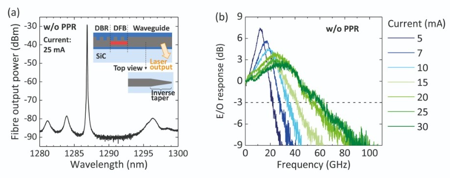
Figure 4. (a) Measured lasing spectrum at 25 mA without using photon-photon resonance. The inset illustrates the laser (cross-sectional view) and provides a top view of the inverse-tapered InP waveguide. The laser light goes through the SiC substrate in the tapered region, which suppresses the reflection at the edge of the waveguide. (b) Measured small-signal electro-optic responses of the laser at various bias currents without using photon-photon resonance.
We bond our InP epiwafers to 2-inch semi-insulating 6H-SiC substrates using oxygen-plasma-assisted direct bonding. This is carried out after sputtering a 20 nm-thick SiO2 layer on both surfaces to yield a total thickness of 40 nm for the SiO2 bonding layer. Note that one of the primary purposes of the 20 nm-thick SiO2 layer is to provide a buffer to plasma damage.
After bonding, we selectively remove the InP substrate, using a combination of an etch stop layer and mechanical and wet etching. Using a SiO2 mask, we define a mesa-stripe structure by dry/wet etching. Burying the active region is followed by using epitaxial growth of undoped-InP, silicon-ion implantation and zinc thermal diffusion to produce a lateral p-i-n junction. Surface gratings are formed on the top, intrinsic InP layer, to define the DFB and DBR sections with lengths of 50 μm and 60 μm, respectively. The final step is to form electrodes on n-InP and p-InP.
Using this approach to fabricate our devices (see Figure 3 (a)), we ensure that the distance between the active region and the 40-nm thick SiO2 layer on the SiC substrate is just 75 nm. This small separation, easy to realise with a thin membrane lateral-current-injection structure, enables effective heat dissipation in the active region. We have been able to fabricate numerous devices on SiC (see Figure 3(b)), indicating the capability of integrating the multi-channel laser array.
Record-breaking speeds
To evaluate intrinsic lasing characteristics without the photon-photon resonance effect, we have fabricated an inverse-taper waveguide, a configuration that ensures that there is no propagation mode in the InP waveguide. With this modification, the optical mode radiates into SiC in the inversely tapered region in InP, resulting in a small-enough reflectivity to suppress the photon-photon resonance (see the inset of Figure 4(a)). This happens because the refractive index of the SiC substrate is higher than that of the SiO2 overcladding layer.
Measurements with an optical fibre reveal single-mode lasing at 25 mA (see Figure 4(a)). This drive current produces a peak output power of 1.20 μW. We attribute this small output power to a large fibre coupling loss, noting that we could not fully detect the radiation mode into SiC. This laser’s threshold current is 2.75 mA.
Encouragingly, our measurements of small-signal electro-optic responses of our laser reveal that the 3 dB modulation bandwidth linearly increases with the square root of the bias current, to reach 60 GHz at 30 mA (see Figure 4(b)). We estimate that the relaxation oscillation frequency is as high as 42 GHz at 30 mA. These are record values for DMLs without the photon-photon resonance effect, indicating that the membrane laser on SiC has an inherent advantage when it comes to increasing the 3 dB modulation bandwidth.
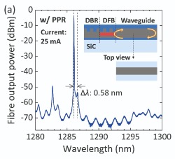
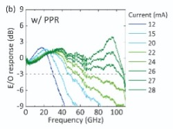
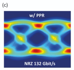
Figure 5. (a) Measured lasing spectrum at 25 mA using photon-photon resonance. The inset illustrates the cross section of the laser and the top view of the InP output waveguide. The waveguide is part of the laser cavity, inducing Fabry–Pérot interference between the front of the distributed feedback section and the edge of the waveguide. (b) Measured small-signal electro-optic responses of the laser without using photon-photon resonance at various bias currents. (c) Equalized optical eye diagram for 132 Gbit/s non-return-to-zero signal.
Driven at 25 mA, this laser exhibits Fabry–Pérot modes in the DFB stopband (see Figure 5(a), and note the contrast with the spectrum shown in Figure 4 (a)).
The free spectral range of the Fabry–Pérot modes is 1.48 nm, corresponding to 270 GHz. At 25 mA the maximum fibre output power is 0.37 mW, and the threshold current 2.54 mA. Based on fitting the spectrum, we estimate the reflectance at the facet of the output waveguide to be about 5 percent.
The photon-photon resonance effect enables far higher data rates. For drive current above 22 mA, small-signal electro-optic responses show a clear photon-photon resonance around 95 GHz, which is not far from the frequency separation of the main lasing and side modes: this is 105 GHz, equating to a value for Dl of 0.58 nm. Thanks to the high relaxation oscillation frequency, along with a photon-photon resonance at 95 GHz, we obtained a flat frequency profile and a maximum bandwidth of 108 GHz.
We have directly modulated our laser with a 132-Gbit/s non-return-to-zero signal, using a back-to-back configuration. This produced a clear eye opening at a bias of 27.2 mA, after equalization with a 61-tap linear equalizer compensating for linear distortion (see Figure 5(c)). Energy cost is not as low as it has been with some of our earlier lasers, coming in at 911 fJ/bit. However, the bandwidth of 108 GHz and the symbol rate of 132 GBaud are more than twice as large as those of conventional DMLs.
Opening the door to applying DMLs to applications beyond 400GbE, our technology is already enabling this class of laser to provide an intrinsic 60 GHz and a photon-photon-resonance-assisted value of over 100 GHz. Plans for the future are to increase the relaxation oscillation frequency and the 3 dB modulation bandwidth, through two strategies: increasing thermal dissipation, by decreasing the bonding SiO2 layer thickness; and increasing the number of quantum wells, to increase the differential gain. With the latter, it’s also possible to reduce nonlinear optical phenomena, which could limit the 3 dB modulation bandwidth at a relaxation oscillation frequency of more than 40 GHz, thanks to a decrease in the photon density in the active region. Working towards this, our next goal is to develop DMLs for high-speed operation under uncooled conditions.
The authors thanks the contributions to this work from Ryo Nakao, Takuro Fujii, Koji Takeda, Tatsurou Hiraki, Takuma Tsurugaya, Shigeru Kanazawa, Hiromasa Tanobe, and Tai Tsuchizawa from NTT.
Optimized high-index contrast gratings provide a thin, highly reflective mirror for specific polarized light
BY KUO-BIN HONG, TSU-CHI CHANG AND TIEN-CHANG LU FROM NATIONAL YANG MING CHIAO TUNG UNIVERSITY
THE ORIGINS of the VCSEL can be traced back to 1977 when Kenichi Iga, working at Tokyo Institute of Technology, proposed this device. Over the intervening years much progress has been made, with this class of laser now well-known for several great attributes, including: a circular beam shape; a low divergence angle; a high speed; a high-bandwidth; and when in the form of an array, a high output power. These strengths have fueled the deployment of this device in optical communications, optical interconnects, high-speed networks, optical clocks, optical mice, laser printing, laser displays, optical gas sensors, and most recently, in 3D sensing.
In a nutshell, the operation of the VCSEL involves the use of a stack of quantum wells to generate light, which bounces back and forth within a very short cavity that has highly reflective mirrors at both ends. This light can be amplified and polarized by stimulated emission from the wells. Common options for a III-V gain medium include InGaN for emission from 400 nm to 700 nm, InGaAs for 850 nm to 1060 nm, and InGaAsP for 1310 nm to 1550 nm. The wavelength of the laser, as well as its longitudinal mode spacing, are controlled by the length of the cavity.
Most established is the GaAs-based VCSEL, a high-performance commercial product. Its manufacture draws on a fully developed epitaxial process, with production benefitting from the combination of GaAs and AlAs, a pairing of materials with an ultralow lattice mismatch and a high refractive index difference – it is more than 0.5. When a distributed Bragg reflector is formed by growing a stack of pairs of GaAs and AlAs layers on a GaAs substrate, it offers a reflectivity close to 100 percent. This aids the formation of the cavity, and simplifies construction of the mirror, arguably the most critical part of the VCSEL.
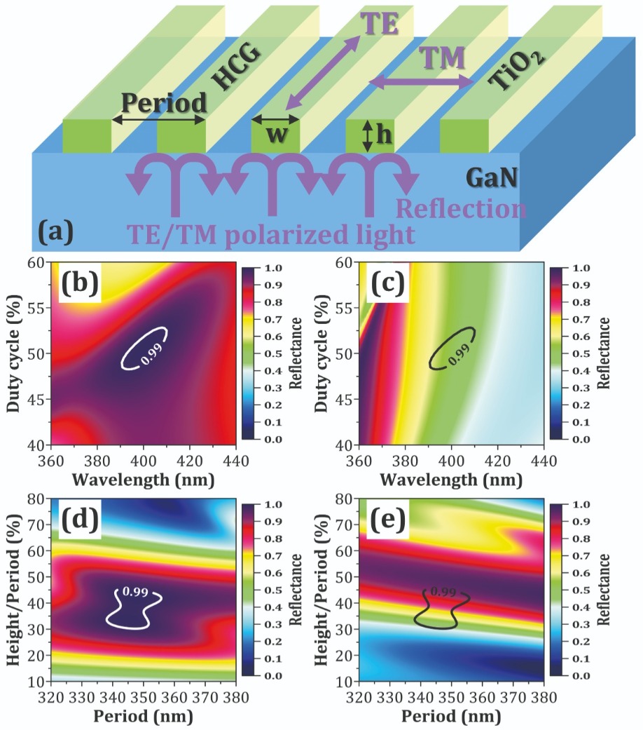
Figure 1. (a) Three-dimensional drawings of TiO2/air high index contrast gratings. (b) and (c), simulated reflectance maps, which are functions of wavelength and duty cycle for incident light with transverse-electric (TE) and transverse-magnetic (TM) polarizations – that is, with electric fields that are parallel and perpendicular to the grating, respectively. (d) and (e) simulated reflectance maps that are the functions of period and grating height for incident light with TE and TM polarization. Contours display the boundaries of the high reflectance zone of up to 0.99-0.999 for TE polarization.
To speed the development and commercialization of the GaN-based VCSEL there needs to be a reliable, straightforward process for producing the mirrors. This is not easy, as the pairing of GaN with either AlN or AlGaN leads to a high lattice mismatch and a low refractive index contrast. A significant lattice mismatch is a major cause for concern: it induces cracks and dislocations that increase carrier leakage paths and trap centres; and it increases non-radiative carrier recombination and irregular light scattering.
One way to side-step all these problems is to switch to a dielectric DBR. In this case, the challenge is to produce a high-reflective mirror with acceptable optical, electrical and thermal characteristics. A popular combination is Ta2O5 and SiO2, a pairing that leads to a huge difference in refractive index. However, these oxides are unsuitable for electrical and thermal conductance. The workaround for addressing the former and realising carrier injection is to deposit a thin layer of ITO between p-doped GaN and the DBR.
When it comes to reducing the thickness of the cavity and flattening the surface of the n-doped GaN layer, prior to the fabrication of the n-side DBR, the most common approaches are laser lift-off and chemical mechanical polishing. With the latter, due to polishing uncertainty, it is hard to precisely control the constant cavity length across the entire wafer.
High contrast gratings
Our team at the National Yang Ming Chiao Tung University, Taiwan, is developing an alternative type of mirror that addresses the limitations of existing designs. We are pursuing a novel reflector that consists of periodic gratings that are orthogonal to the direction of the laser’s emission. These gratings, with a sub-wavelength period, height and width, use two dielectrics – or semiconductors – with markedly different refractive indices. Reflectors based on high-contrast gratings, featuring dielectric/air interfaces, possess several excellent features, including a sub-wavelength thickness and a polarization-dependent reflectivity spectrum with a wide stopband.
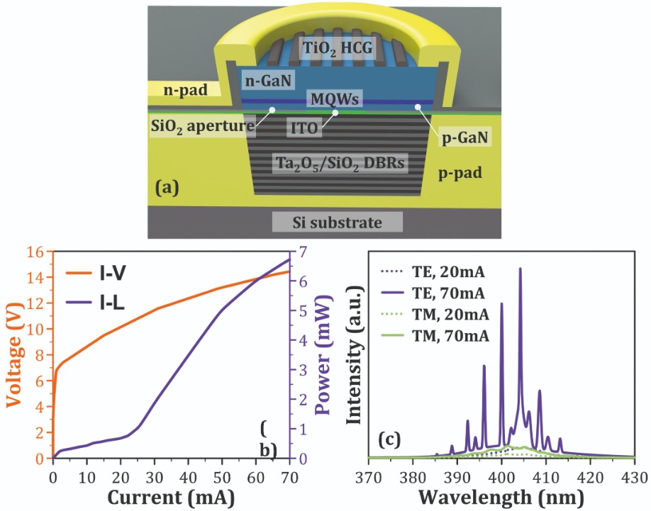
Figure 2. The cross-sectional view of an electrically-pumped VCSEL combined with TiO2 high index contrast gratings. (b) Measured light-current-voltage (L-I-V) curve of a GaN-based VCSEL integrated with TiO2 high-contrast gratings. (c) TE- and TM-polarized emission spectra of a GaN-based VCSEL integrated with high-contrast gratings operated at 20 mA and 70 mA.
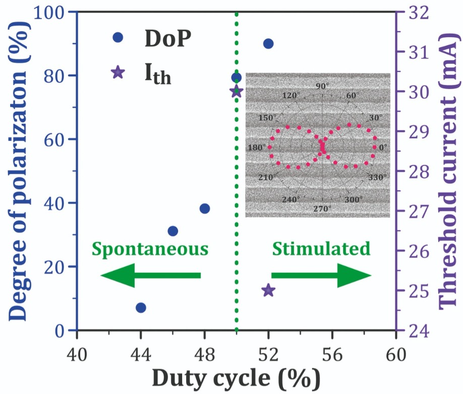
Figure 3. Measured degrees of polarization (DoP) and threshold current (Ith) of electrically-pumped GaN-based VCSELs combined with TiO2 high-contrast gratings for different duty cycles. Insets show the polarization of the laser beam and a scanning electron microscopy image of TiO2 high-contrast gratings. The direction of polarization highly coincides with the gratings.
Efforts by our team at designing and developing a high-reflective high-contrast grating mirror for a particular transverse-electric or transverse-magnetic polarization began with calculations. This involved a combination of rigorous coupled-wave analysis, coupled mode theory, and finite-difference time-domain and finite element analysis.
Using two-dimensional finite element analysis, we produced high-resolution reflectance maps of periodic TiO2 high-contrast gratings as functions of wavelength, period, grating height and duty cycle (defined as the grating width, divided by the period) for light with transverse-electric and transverse-magnetic polarizations, exciting from the bottom surface of GaN (see Figure 1). We found that commercial finite element analysis software provided us with an easy, convenient tool to help us swiftly acquire the numerical data of high-resolution reflectance maps.
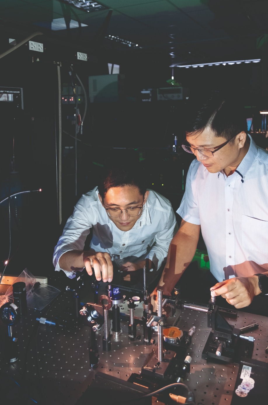
The numerical tools at our disposal enabled us to produce contour plots that express the boundaries of the transverse-electric-polarization reflectance zone of up to 0.99-0.999 (see Figures 1(b) to 1(e)). According to this modelling, the highest reflectivity for light with transverse-electric polarization is twice that of light with a transverse-magnetic polarization.
Based on the insight provided by our numerical tools, we have targeted TiO2 gratings with a period of close to 344 nm, a duty cycle of 52 percent, and a grating height of 112 nm – that is equal to 32.6 percent of a period – as the starting point for the development of a high-reflective high-contrast grating mirror.
Fabrication of our high-contrast gratings began by sputtering a TiO2 layer on the top surface of GaN and patterning this with e-beam lithography. According to atomic force microscopy, the polished GaN had a surface roughness of approximately 0.67 nm. After etching, inspection with a transmission electron microscope revealed that some dimensions differed a little from the target thickness. The actual height of the grating is 112.3 nm; and its width is 177.8 nm, corresponding to a duty-cycle of 51.6 percent, for the measured period of 344.5 nm. Fortunately, the dimension of the fabricated high-contrast gratings falls within the high reflectance zone.
VCSEL integration
We have undertaken a variety of measurements on one of our VCSELs, which has a 10 μm-diameter, circular current aperture and a top TiO2 high-contrast grating mirror (see Figure 2 (a) for details of its design). We have recorded light power-current-voltage characteristics (see Figure 2(b)), polarization-resolved emission spectra for different current-injection conditions (see Figure 2(c)), and the associated degree of polarization (DoP) for different duty cycles (see Figure 3).
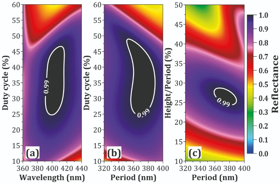
Figure 4. Simulated reflectance maps are functions of (a) wavelength and duty cycle, (b) period and duty cycle and (c) the period and grating height of a monolithic GaN high-contrast grating for incident light with TE polarization. Contours indicate the boundaries of the high reflectance zone of up to 0.99-0.9999.
Measurements on our devices reveal a lasing threshold current of 25 mA and a corresponding current density of about 32 kA cm-2, under the driving conditions of a pulse width of 0.1 μs and duty cycle of 0.3 percent. We have also recorded transverse-electric and transverse-magnetic polarized emission spectra at different current-injection conditions by placing a polarizer between the optical fibre and the VCSEL. These spectra provide strong evidence of a transverse-electric-polarized laser beam. In good agreement with the prediction of the high-reflectance zone (see Figure 1(b)), the dominating lasing peak occurs at 404.2 nm.
We have studied the threshold currents and associated degrees of polarizations for a range of VCSELs with different duty cycles. For this investigation, we defined the degrees of polarization as (Imax – Imin)/(Imax + Imin), where Imax and Imin are the maximum and minimum values of measured light intensities for a 60 mA injection current. We have found that our VCSELs only produce lasing action when they have a duty cycle of either 50 percent or 52 percent; for these devices, the degrees of polarization for the transverse-electric laser beams are 80 percent and 90 percent, respectively. Our VCSELs with TiO2 high-contrast gratings with lower duty cycles – values of 44 percent, 46 percent and 48 percent – only produce spontaneous emission, because the gratings have a lower reflectivity, causing increases in mirror loss and scattering loss. One possible option for reducing the absorption loss of the TiO2 high-contrast grating while simplifying the fabrication process is to switch to a GaN-based monolithic high-contrast grating mirror.
Monolithic high contrast gratings
Several technologies are available for depositing the thin films needed to form a grating, including spin coating, sputtering, ultrasonic spray pyrolysis and atomic layer deposition. One way to judge the optical quality of the films produced by these methods is to measure the extinction coefficient, also known as the absorption coefficient. Process conditions impact this. For example, when a TiO2 film is prepared by spin coating and sputtering, it can have an absorption coefficient up to 10,000 cm-1, but when added by atomic layer deposition, this value can be as small as 200 cm-1 for wavelengths close to 400 nm. When viewed in this manner, monolithic GaN offers much promise as an alternative to TiO2 for forming a high-contrast grating that provides an ultralow absorption mirror.
The suite of numerical tools at our disposal have enabled us to assess the potential of monolithic GaN for high-contrast gratings. Armed with these insights, we have identified the fabrication window with highest reflectance by calculating transverse-electric-polarized reflectance maps for various incident wavelengths, periods, duty cycles, and grating heights (see Figure 4). Again, we plotted contours that indicate the boundaries of the high reflectance zone, this time with values ranging up to between 0.99 and 0.9999.
This exercise identified a widespread zone with a peak reflectivity up to 99.99 percent close to 403 nm, as well as a stopband with a width near 25 nm. It is encouraging that there is more tolerance to variations in the duty cycle from its target value when working with a GaN high-contrast grating mirror, rather than one made from TiO2 or related materials.
According to preliminary results, our GaN VCSELs featuring monolithic GaN high-contrast gratings exhibit superior characteristics. We plan to put this to the test, making VCSELs with a GaN high-contrast grating for the p-type reflector that will drive a further reduction in cavity length, alongside increased heat dissipation for this device.
Detailed design principle and theory of high-contrast gratings can be found in the following papers:
Fabrication and characteristics of TiO2 gratings and related metasurfaces can be found in the following papers:
Design, fabrication and characteristics of monolithic GaN high-contrast gratings can be found in the following papers:
Fabrication, measurement and characteristics of GaN-based VCSELs with high-contrast gratings and other related materials can be found in the following papers:

According to Precedence Research in a report from January 8, 2021, the global electric vehicle market is expected to grow by more than 40% by 2027. What it says, among other things, is that the supply chain for chips and modules powering these vehicles needs to evolve immediately. One of the obvious shifts will be moving away from traditional devices made from silicon and toward devices made from compound semiconductor materials such as silicon carbide (SiC). At higher voltages needed for EV’s, the performance properties of SiC far outpace those of silicon, but the supply chain for SiC is not nearly as mature. The global EV market needs SiC to catch up…and quickly.
Integrated Device Manufacturers (IDMs), already well-versed in silicon, needed a pathway to produce SiC devices and modules for rapidly accelerating EV demand. But SiC is more complex because it comes from a crystal that is extremely difficult to grow, and that presented a bottleneck. It is against this backdrop that GTAT (www.gtat.com) began forging a business model in 2017 to become a ‘pure-play’ producer of wafering-ready SiC. The Company’s focus on growing SiC bulk crystal and staying away from wafering and device-making is an important distinction. “We have a core competency, and that’s crystal growth,” says GTAT President and CEO Greg Knight. “There are tremendously talented companies around the world that know how to make wafers and devices, but what they don’t necessarily have is a way to grow the SiC crystal. They need the material, and lots of it.”
GTAT’s heritage as a producer of crystal growth equipment means that it can ‘scale up’ capacity very rapidly. The knowhow needed to design and build crystal-growth furnaces is the essence of GTAT’s DNA. “We are able to bring SiC capacity to market faster than anyone,” said Knight. Indeed, the Company has hit milestones extraordinarily rapidly. “We made our CrystX® silicon carbide n-type material available to customers in 2018, less than a year after opening our facility,” said Knight. A year after that GTAT achieved ISO 9001:2015 certification and signed the first of several long-term supply agreements with key customers for 150mm diameter boules.
Fundamentally, SiC is not a defect-free material and is challenging to make at the high quality levels customers demand. That is why most of the companies invested in making SiC wafers and devices do not have the experience to also make the crystal material itself. The equipment used to make silicon cannot be used for SiC, and the capex (and time) required to develop in-house SiC growth is significant. “We understood this early-on,” said Knight. “We knew that SiC was going to become the base material for semiconductors used in growing applications such as EV.”

Specifically, Etch Pit Density (EPD) and Basal Plane Dislocations (BPD) are critical quality metrics for SiC. GTAT has made significant progress driving down BPD’s to less than 1,000 per cm2 and is set to reduce this by another 50% in the near term. Much of GTAT’s focus has been on reducing defects through continuous improvement. “This is what our customers demand, and we deliver,” said Knight.
“We have a longstanding heritage in building the equipment we now use ourselves, and we couple that with a high level of process excellence.” GTAT’s inherently stable production process enables all its high-quality material to be made to this standard, which is available under a single product grade.
While continuous improvement is a function of GTAT’s increased cycles of learning and optimization, R&D efforts allow the company to push forward on 200mm diameter SiC as well as semi-insulating (SI) SiC for RF applications. Both product launches are expected in late 2021 or early 2022. To support existing 150mm demand while forging ahead with 200mm and SI, GTAT is currently growing production capacity by 60% on top of what exists today. With multiple supply agreements in place, the ability to ramp up quickly puts GTAT in a perfect position. “Rapidly growing markets like EV require a very nimble supply chain, and we’re able to respond,” said Knight. This round of expansion will be completed by early Q3 2021, with more expected as partners continue to scale their demand.

Introduction of 200mm diameter. SiC will occur later in 2021
The 78% increase in wafer surface area means a corresponding increase in the number of devices, which helps lower cost. “Higher quality and bigger-diameter boules are parallel efforts for us,” said Knight. “We are moving very rapidly in response to a very dynamic and fast-growing set of markets.”

GTAT will be expanding its production capacity by 60 percent in 2021.
From EV’s to 5G, the global push to ‘electrify everything’ is resulting in a need for circuits and devices that have performance capabilities that extend well beyond those afforded by silicon. While SiC is seen as a front-running material to meet this challenge, demand for it far exceeds supply. This is because most producers of silicon cannot add SiC to their portfolios without investing in an entirely new process and undergoing a very steep learning curve. This is where a ‘pure-play’ SiC producer such as GTAT becomes valuable on a global scale. As GTAT boosts the ‘non-captive’ global supply of high-yield, high-quality SiC, devices made from SiC become more affordable. This means higher performance and lower system-level costs. In practical terms, EVs can enjoy better range thanks to increased use of more electrically efficient SiC. Also, the affordability index for EVs will increase over time as SiC becomes more prevalent.

GT Advanced Technologies is a manufacturer of high-performance crystal materials including silicon carbide (SiC) and sapphire. GTAT’s corporate headquarters in Hudson, New Hampshire also serves as the Company’s primary manufacturing facility for its CrystX silicon carbide. This material is fundamental to the production of semiconductors used in electric vehicles and other power electronics applications.
Directly contact:
Christopher Van Veen
chris.vanveen@gtat.com for more information, or visit us at:https://gtat.com/products/silicon-carbide

Driving down carbon contaminations and cranking up silicon trims the operating voltage of deep-UV LEDs with a tunnel junction
A JAPANESE COLLABORATION is claiming to have broken new ground for reducing the operating voltage of tunnel-junction deep-UV LEDs. Success has come from suppressing the incorporation of carbon contaminants in an n-type AlGaN layer that is then doped with a high concentration of silicon.
The lower operating voltage promises to increase the optical efficiency of high-power tunnel-junction LEDs, which will become the dominant form of this device, according to Kengo Nagata, spokesman for the team. Nagata, who is affiliated to Nagoya University, Toyoda Gosei and TS Opto, told Compound Semiconductor that it is extremely difficult to realise an ohmic p-type AlGaN contact. “We believe that the tunnel-junction LED is one of the device structures that solves this problem.”
Note that switching to GaN for the p-contact is not a viable option. GaN would absorb light emitted by the quantum well, and drive down the light extraction efficiency for the deep-UV LED.
To uncover good growth conditions for lowering the operating voltage of deep-UV LEDs with a tunnel-junction, the team from Nagoya University, Toyoda Gosei, TS Opto and Meijo University produced a portfolio of devices. As well as making a pair of devices with a p-n junction that has different aluminium concentrations in the p-AlGaN layer, they fabricated five devices with tunnel junctions containing differing levels of carbon and silicon concentrations in the n+ AlGaN and top n-AlGaN layers (see Figure for details of both structures).
All these forms of deep-UV LED were produced on sapphire substrates with a 3 μm-thick AlGaN template that had screw and edge dislocation densities of 9 x 107 cm-2 and 1 x 109 cm-2, respectively. On this the team added an n-type Al0.38Ga0.62N underlayer, with screw and edge dislocation densities of 1 x 108 cm-2 and 9 x 108 cm-2, followed by an active region with 2 nm-thick Al0.45Ga0.55N quantum wells and an electron-blocking layer.
After adding either a p-GaN/AlGaN structure or a tunnel-junction, 1 mm2 LEDs were formed by using dry etching to define a mesa, prior to adding contacts. A stack of metals provided both of the n-AlGaN contacts for the tunnel-junction LED, as well as the n-AlGaN for the p-n LED; while an indium zinc oxide layer provided the p-GaN contact for the p-n LED.
Current-voltage plots for the p-n junction LED produced typical results for this class of device, with a forward voltage of 6.6 V at 63 mA cm-2.
Comparing current-voltage characteristics for a variety of deep-UV emitters with tunnel-junctions revealed that a reduction in the level of carbon contaminants, realised by lowering the growth pressure from 100 mbar to 50 mbar, reduced the operating voltage by more than 6 V. Combining this with a high silicon-doping concentration in the n+ AlGaN layer led to an additional and significant reduction in operating voltage to 10.3 V at 63 mA cm-2. Getting the level of carbon contaminants down proved crucial, because it prevented the AlGaN layer from being semi-insulating – that is a show-stopper for forming a tunnel junction.
Optical measurements showed that the conventional UV LED produced an output of 35.7 mW at 285 nm, for a drive current density of 63 mA cm-2, realised at 7.2 V forward voltage. The tunnel-junction device providing a comparison realised an identical drive current at 10.8 V, and delivered an output of 27.6 mW, for a peak emission wavelength of 280 nm. The team attributed this inferior performance to high absorbance by the n-type electrodes, which were sintered at a high temperature.
Nagata says that one of the goals for the team is to extend the optimisation of the tunnel junction, with efforts directed at improving the growth conditions for other layers. “In addition, we will take on the challenge of improving device characteristics, using reflective electrodes.”
Reference
K. Nagata et al. Appl. Phys. Express 14 084001 (2021)
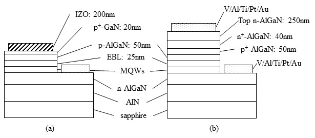
The epistructure used for conventional deep-UV LEDs and those with a tunnel junction.

A sputtered layer of p-type NiO nearly doubles the blocking voltage of GaN-on-silicon Schottky barrier diodes
Engineers from EPFL, Switzerland, are claiming to have broken the record for the breakdown voltage of GaN-on-silicon Schottky barrier diodes. The team’s devices, featuring a p-type NiO layer that acts a junction termination extension, are capable of blocking up to 443 V.
Junction termination extensions are common structures, widely deployed in silicon and SiC devices to prevent localised peaking of the electric field and ultimately ensure a higher blocking voltage.
However, in those devices the junction termination extensions are formed by implantation or diffusion, to create selectively doped regions. With GaN, ion implantation is still in its infancy, requiring pressures of more than 1 GPa and temperatures above 1200 °C.
To side-step issues associated with ion implantation, the researchers at EPFL, led by Elison Matioli, have switched to RF sputtering of NiO, a p-type conductive oxide that can realise high hole densities. Note that in 2020, researchers at Nanjing University and at Sun Yat-sen University both reported the use of doped NiO to realise a high reverse-blocking voltage in Ga2O3, despite the large band offset between these two materials. “This inspired us to evaluate the use of p-NiO as junction termination extensions for GaN power devices,” says Matioli.
He and his co-workers are not the first to report the addition of p-NiO junction termination extensions to GaN Schottky barrier diodes. Earlier this year, a team led by researchers at Tokushima University, Japan, announced the fabrication of devices with this architecture. Using bulk GaN substrates and a 14 μm-thick drift layer, they realised a blocking voltage of less than 250 V.
The higher blocking voltage is likely to partly result from the switch from a TiN anode that has a Schottky barrier height of 0.6 eV to a nickel anode with a height of 0.9-1 eV. There may also be differences in the design and fabrication of the diodes. “We spent a considerable amount of time optimising the design of the junction termination extension, the deposition conditions of p-NiO, as well as perfecting the fabrication process for our device,” says Matioli.
The team’s devices were fabricated from 150 mm GaN-on-silicon epiwafers, provided by Enkris. These epiwafers had a 1.1 μm-thick buffer, followed by a 1 μm-thick layer of n-type GaN and a 4 μm-thick layer of intrinsic GaN. At EPFL, engineers added a 160 nm-thick layer of NiO by RF sputtering, before using a lift-off process to define the junction termination extension region. To complete diode fabrication, the engineers used Ni/Au to form a p-type ohmic contact, before creating a mesa with reactive-ion etching that enabled access to the n-type layer – this facilitated the addition of Cr/Au to create an n-type ohmic contact.
Current-voltage measurements on a conventional GaN Schottky barrier diode, grown as a control, and the variant with the junction termination extension, show that this modification does not have a significant impact on the on-resistance or the turn-on voltage. However, the blocking voltage has a substantial increase, rising from 230 V to 443 V.
The team is aiming to make additional improvements to its p-NiO deposition conditions. Efforts will focus on RF sputtering power and ambient gas flux, as this could reduce the reverse leakage current at the p-NiO/GaN interface. “This will help us achieve a variety of devices, like merged p-i-n Schottky diodes, junction barrier Schottky diodes, as well as JFETs,” says Matioli.
Reference
R. Khadar et al. Appl. Phys. Express 14 071066 (2021)
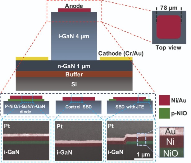
Three variants of the diode were produced: one with a p-NiO layer, to enable study of transport properties; a control; and a Schottky barrier diode (SBD) with a junction termination extension (JTE). Focused ion-beam cross-sectional scanning electron microscopy images of the regions depicted in the blue boxes.

Low-temperature MOCVD re-growth creates Ga2O3 MESFETs with record-breaking currents and on-off ratios
A COLLABORATION between engineers at the University of Utah and The Pennsylvania State University claims to have produced the first fully MOCVD-grown β-Ga2O3 MESFETs with ohmic contacts.
Spokesman for the team, Sriram Krishnamoorthy from the University of Utah, told Compound Semiconductor that a major bottleneck for re-growing ohmic contact is the need for high temperatures, to ensure high-quality material. These high temperatures threaten to degrade the channel. “We came up with a solution and demonstrated high-quality β-Ga2O3 growth using MOCVD at a temperature of 600 °C, which is more than 200 °C lower than the conventional growth temperatures for MOCVD Ga2O3 growth.”
As well as reducing the thermal budget, the lower growth temperature opens up avenues for hetero and hybrid integration with other semiconductor materials that require lower processing temperatures.
Growth of β-Ga2O3 at lower temperatures also enabled controllable doping over four orders of magnitude, and doping profiles ten times sharper than before. “This could help in the development of high-efficiency Ga2O3-based lateral RF devices through delta doping and modulation doping schemes,” argued Krishnamoorthy.
The team produced their devices using a Agnitron Agilis MOCVD reactor, which is specifically designed for high-quality growth of β-Ga2O3 material on wafers with sizes up to 2 inch. Efforts began by taking iron-doped semi-insulating β-Ga2O3 substrates produced by NCT, Japan, cleaning their surface by dipping them in a dilute HF solution for 30 minutes, and then loading this material into an MOCVD chamber and depositing a 500 nm-thick β-Ga2O3 channel at 810 °C. Device mesas were defined by a hard mask and dry etching, before a selective area MOCVD regrowth process provided low ohmic resistance source and drain contacts.
Formation of these contacts began by adding a 500 nm-thick sacrificial layer of SiO2 by plasma-enhanced CVD. The source and drain regions were defined using a nickel layer patterned by photolithography and lift-off. Reactive ion etching selectively removed the SiO2, plus 10-20 nm of Ga2O3.
Dipping the sample in aqua regia solution removed the nickel mask, before the growth of silicon-doped Ga2O3 at 600 °C. The next steps involved removing the polycrystalline Ga2O3 outside the contact region by dissolving the sacrificial SiO2 in HF solution, and using photolithography and patterning to add metallic contacts to the regrown contacts. Adding a metal stack for the Schottky gate completed fabrication.
According to the team, electrical measurements on their MESFETs revealed a record sheet resistance of 73 W/square for silicon-doped β-Ga2O3 regrown layers, and a record-low specific-contact-resistance of 8.3 x 10⁻⁷ W cm2 for the metal/ b-Ga2O3 contacts. The on-current hit 130 mA m-1. “This is the highest [value] for a depletion mode β-Ga2O3 MESFET with an on-off ratio of over 1010, simultaneously in a large gate length device,” said Krishnamoorthy.
He explained that β-Ga2O3 lateral FETs suffer from an off-state leakage through the epilayer/substrate, due to residual silicon impurities. It is speculated that this problem originates from the wafer polishing process. “We have demonstrated an efficient way to suppress off-state leakage using pre-growth wafer cleaning, but have preserved the high-mobility of carriers in the MOCVD-grown channels.”
One goal is to now develop β-Ga2O3 scaled devices using MOCVD-grown channels that would leverage the high mobility of carriers for high-frequency applications. “We would also like to work on electric-field management techniques to further enhance the breakdown performance of MOCVD-grown β-Ga2O for high-power applications,” added Krishnamoorthy.
Reference
A. Bhattacharyya et al. Appl. Phys. Express 14 076502 (2021)
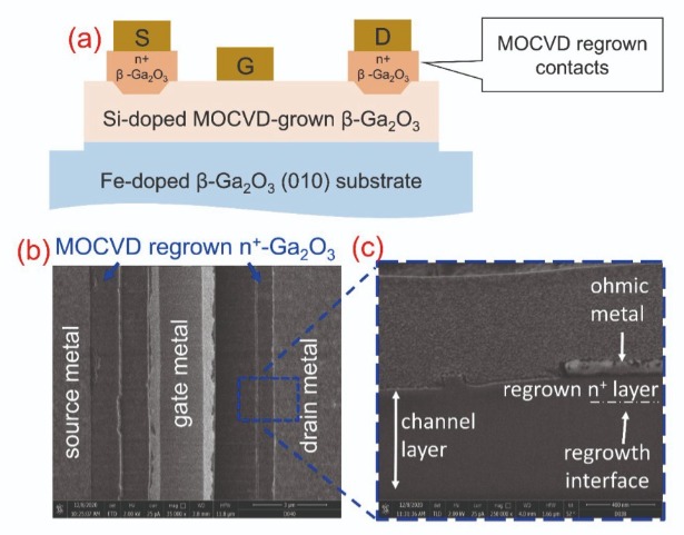
(a) Fully MOCVD grown MESFETs with regrown ohmic contacts. (b) Top view, scanning electron microscopy image of the MESFET, showing the re-grown access regions. (c) Cross-sectional scanning electron microscopy image of the contact region.
