


There’s no doubt that a successful device doesn’t have to be perfect. Take the LED: despite numerous defects, it nets billions of dollars every year, thanks to its deployment in backlights and light bulbs. And then there’s the device of the moment, the SiC MOSFET. Spurred on by soaring sales of electric vehicles, its revenue is climbing fast, despite a resistance that is an order of magnitude higher than it ought to be.The failure of the SiC MOSFET to deliver its true potential stems from a weakness at the interface between SiC and its native oxide. In this form of MOSFET, the semiconductor-oxide interface is far from ideal – it is riddled with traps that hold back channel mobility to just a few percent of the bulk value.
Formation of the oxide in today’s commercial SiC MOSFETs is based on a process that goes back 20 years. The drawbacks of this process are well known, but despite much effort, for the majority of the intervening years no substantial progress has been made in developing a better alternative. Some approaches initially offered much promise, but weaknesses surfaced when devices were subjected to greater scrutiny, such as a threshold-voltage instability and a short oxide lifetime.
Now, progress is finally being made, thanks to the work of a team at Kyoto University, Japan. These engineers, led by Tsunenobu Kimoto, have come up with not just one, but two related technologies to produce a high-quality semiconductor-oxide interface in the SiC MOSFET.
Key to the team’s success has been efforts into fathoming the imperfections at the conventional interface between SiC and its native oxide. Scrutinising samples revealed that while oxidation removes the majority of carbon atoms, some remain near the interface, causing defect formation.
As these defects can be up to 5 nm or so below the surface, the processes developed by Kimoto and his co-workers begin by etching the samples with hydrogen gas. After this, either silicon is deposited and converted to SiO2 by low-temperature oxidation; or SiO2 is deposited. In both cases, nitridation follows, either with nitrogen gas or NO, to passivate some of the defects at the interface.
Results are encouraging, trimming the defect density at the interface and doubling the mobility in the channel, realised at a high gate voltage.
The team’s success has not gone unnoticed. Some chipmakers have already started to transfer a superior process to their fabs. Once they start to churn out better MOSFETs, the performance gap between these devices and those based on silicon will grow even wider, helping to spur further sales. While a device doesn’t have to be perfect to net significant revenue, improving its performance is sure to lend a helping hand.
The recently launched Photonic Integration Technology Center in The Netherlands is set to take the nation’s thriving industry to global markets, reports REBECCA POOL
AS THE PHOTONIC INTEGRATED CIRCUIT (PIC) market gathers momentum, industry players are eyeing The Netherlands with growing interest. In only the last year, two Dutch photonic chip companies have raised more than Ä60 million in investment funds to kick-start photonic chip manufacturing.
In June 2020, independent PIC foundry, Smart Photonics received Ä35 million to expand its wafer manufacturing capacity at the High Tech Campus in Eindhoven. And in March, this year, PIC manufacturer Effect Photonics also won $37 million – around Ä30 million – to develop single-chip coherent optics and scale production.
In addition, in late 2019, PhotonFirst – previously called Technobis – scooped an undisclosed sum to ramp production of its integrated photonic sensors. And recently, Surfix won Ä8.5 million to accelerate development of its integrated photonic biosensing platform.
But the industry buzz doesn’t stop here. Only weeks ago, integrated photonics industry accelerator, PhotonDelta, Eindhoven University of Technology, also known as TU Eindhoven, the University of Twente and research institute TNO, joined forces to launch the Photonic Integration Technology Center (PITC).
As Sylwester Latkowski, PITC scientific director and TU Eindhoven researcher, tells Compound Semiconductor: “We have Smart Photonics, Effect Photonics and PhotonFirst all of which have PICs at the heart of their business and products.”
“More and more customers are approaching these companies, and as fantastic and leading edge are their products, scaling up manufacture isn’t always simple,” he adds. “We’ve seen a need to mature certain aspects of the PIC technologies and supply chain, and will work with businesses to get the next generation products production-ready.”
Europe and beyond
As well as these key Dutch businesses, PITC is also working with testing company, Salland Engineering, PIC design house, Bright Photonics, VTEC Lasers & Sensors and more.

Testing times at PITC: photonic IC on an evaluation kit.
However, Latkowski is keen to emphasise the centre’s international outlook, pointing to partnerships with France-based optical spectrum analyzer and automated optical test equipment supplier, APEX Technologies, German photonics assembly and testing company, ficonTEC, and potential US-based collaborations in the future.
The PITC scientific director also likens the newly-launched PITC to the Belgium-based R&D hub, Imec, emphasising the value that such an organisation can bring to a supply chain. “Such an overarching centre can perfectly co-exist alongside established institutes, companies, large industry and universities,” he says.
PITC was conceived by Erik Van Geest from PhotonDelta, TNO’s Jan-Laurens van der Steen, Pieter Telleman, University of Twente and of course, Latkowski. As such, the centre is home to a broad photonics-related expertise. Latkowski and colleagues at TU Eindhoven, including Kevin Williams, have spent years working on active-passive monolithic InP integration, creating lasers, amplifiers, quantum well modulators, detectors and more on a chip.
Meanwhile, Twente University provides expertise in SiN-based technologies, with spin-out LioniX International designing and fabricating PICs, and delivering SiN waveguides and modules to market. Still, as Latkowski emphasizes: “We also work with silicon photonics, and as an organisation, PITC is technology-agnostic.”
At the same time, TNO brings industry experience in maturing technologies. And PhotonDelta, a public-private partnership of government agencies and integrated photonics modules players, has contributed significant funds, alongside other organisations.
Indeed, PhotonDelta members include researchers, chip designers, foundries and software developers, that develop single and hybrid InP and SiN waveguide technologies. For example, Bright Photonics, Effect Photonics, Lionix International, PhotonFirst, Surfix, SmartPhotonics and VTEC are amongst the numerous industry partners from The Netherlands, with other partnering organisations including the European Photonics Industry Consortium and the MESA+ Institute of Nanotechnology.
From the outset, PITC will focus on increasing its partners’ Technology Readiness and Manufacturability Readiness Levels. Latkowski points to how the centre could help a company such as VTEC Lasers & Sensors, which develops pluggable modules for telecoms suppliers, to reduce its design-in window and have products ready on demand with the necessary specification.
“Customers like VTEC have mature products but have to hit certain deadlines when manufacturing at volume,” he says. “The telecoms industry doesn’t wait for anyone, but we can help them meet the necessary time-frames.”
PITC is going to focus on several key programmes, including metrology, InP, SiN and hybridization. As well as leading PITC scientific activities, Latkowski also chairs the photonic test technical working group at IPSR-I – Integrated Photonics System Roadmap-International – that created the reference document to shape the future of the PIC. Given this, he is particularly passionate about metrology. “Years ago, PIC roadmapping activities from MIT indicated that test, assembly and packaging are the dominant cost drivers for a PIC-based module... and today’s PICs are much more complicated,” he says.
“While packaging and assembly is more of a challenge, we have companies that offer this but when it comes to testing, no-one really is keen to do this, and it isn’t trivial,” he adds.

Industry grade fully automated die tester being developed together with Ficontec in PIXAPP and InPulse pilot lines.
“There’s a lot to be done,” he says. “We’re proposing to work with multiple parts of the supply chain, including OEMs, fabs, and equipment and software vendors, on this as there are no comprehensive test tools yet.”
In a similar vein, Latkowski asserts that hybridization is key. “I’m strongly pushing this [PITC programme line],” he says. “The PIC module is typically a hybrid and includes some combination of InP, SiN, silicon and electronics, not just photonics.”
Tech-development aside, Latkowski and PITC colleagues will also be developing a future workforce for the photonics industry. Latkowski reckons that today, the pool of engineers and researchers with photonics expertise is somewhat limited. However, he will be working with partners at the Fontys University of Applied Sciences, home to more than 44,000 students based in and around Eindhoven.
“Existing candidates typically hold a PhD [relevant to photonics] but this may not always be what is needed to fill a vacancy,” he says. “We will shape teaching and internship programmes for the future talent that industry needs – this could be electronic-photonic test engineers and photonic product designers.”
“Importantly, every PITC launch partner has already expressed an interest in supporting and taking part in these programmes,” he adds.
Along the way, the centre leaders intend to stay abreast of the latest industry technology developments. Pointing to polymer optics developments, largely driven by Michael Lebby, chief executive of Lightwave Logic, Latkowski says: “We have research activities in materials such as this and are watching how these evolve.”
“If these are seen to be attractive to module suppliers, we will be able to help here, and will monitor technologies such as this that may be needed for the next generation of photonics products,” he adds.

Sylwester Latkowski, PITC scientific director, has much experience in developing photonic circuits, having spent many years as a researcher at the TU Eindhoven.
Hybrid bonding provides attainable scaling for packaging of compound semiconductor devices in copper or gold
BY JOHN GHEKIERE FROM CLASSONE TECHNOLOGY
FABRICATING semiconductor devices begins by growing epiwafers, with efforts directed at ensuring high-quality crystalline material with minimal imperfections. Once a device is completed, it often has to be integrated into its CMOS brain in order to carry out its impressive tasks. Commonly this integration is accomplished by employing advanced packaging techniques, many of which include some form of pillar formation and bonding. However, continued input/output (I/O) scaling is taking conventional packaging approaches and putting them out of reach for many manufacturers. Hybrid bonding offers abundant opportunity for I/O density scaling.
Increasing in popularity, heterogeneous direct bonding, also known as hybrid bonding, is a technology that involves directly bonding dielectric and interconnect features, either between two wafers, or between a chip and wafer. Such a concept is not new, having been studied and developed over the course of more than a decade, and already deployed in the manufacture of some CMOS image sensor devices. Yet, until recently hybrid bonding has not gained widespread traction as a viable approach for packaging integration. But that is changing.
The exponentially increasing technical difficulties associated with the scaling more well-established approaches, primarily based on pillars, has driven interest in hybrid bonding, along with a hike in its funding. The challenges of scaling that are facing leading-edge pillar applications are so great that they are putting enabling input/output density scaling out of the reach for most device manufacturers.

This limitation is a major blow for compound semiconductor device manufacturers operating in this highly competitive marketplace. As the majority of dollars spent on development are largely committed to true device technology, there is little funding left to try and advance an already profoundly advanced packaging flow. Adding to the woes of the compound semiconductor industry are the relatively small R&D budgets compared with those of the manufacturers of silicon-based devices. Foundries are an option, but as compound semiconductor devices are still largely produced on wafers with a diameter of 150 mm or less, finding a foundry operating at these wafer diameters and yet capable of such advanced packaging integration is becoming impossible.
Fortunately, hybrid bonding offers a genuine alternative. This approach is clearly important, justifying expenditure on development that should offer a great return. While some investment optimisation is valuable, there is the promises of multiple generations of incremental innovation, an attractive proposition compared with the diminishing returns that characterise further pillar development.

Direct bonding of gold pads for emerging devices.
Can such coplanarity be achieved? At present, yes, and great achievements are continuing in this regard. But each new scaling requires development of new plating chemistries and equipment modifications, alongside a level of novelty in innovation that tends to result in new patents and exclusive IP. All of which means more cost. Can it be done? Yes – and it is being done. However, given the growing difficulties, progress that is demanded is inaccessible to all but a few manufacturers.
There are also challenges to conventional packaging that go beyond plating and mechanical integrity. Consider lithography. The photoresists used in pillar/bump packaging integration are just one of the many marvels produced in the semiconductor industry. They have to be compatible with a multitude of plating electrolytes with values for pH ranging from just 1 or 2 to as high as 9 or 10; a genuine compatibility challenge for resist formulation. There is a trade-off when using a highly robust resist material. It creates challenges for removal, solved using processing steps that are chemically and mechanically aggressive. Again, does it work? Yes, so far. However, it serves to further narrow an already narrow process window that arises because the plated features, composed of multiple metals (think adhesion), are incredibly small, free-standing structures. There are also practical considerations associated with the sheer precision of the feature dimensions of a photoresist operating at these sizes. Progress is being made, but these advances are coming from fewer and fewer manufacturers.
Hybrid heaven
Switching from the use of pillars to hybrid bonding greatly simplifies many of the issues that are associated with plating, mechanical integrity and lithography. For starters, hybrid bonding employs plating capabilities that have already been established for far smaller feature sizes and a narrower pitch. Take copper metallization, the most common implementation of hybrid bonding: CMOS interconnects have already driven the development of feature fill plating to dimensions below 100 nm, which is more than three orders of magnitude smaller than that associated with pillars. What’s more, this drove the filling of much higher aspect ratio features than those required for hybrid bond applications. When focusing on plating, we can see that the advances necessary for four, five or even six additional generations are already largely established and feasible. The CopperMax reactor from ClassOne Technology represents an advanced plating cell designed to deliver such extensibility in copper fill for hybrid bonding applications.
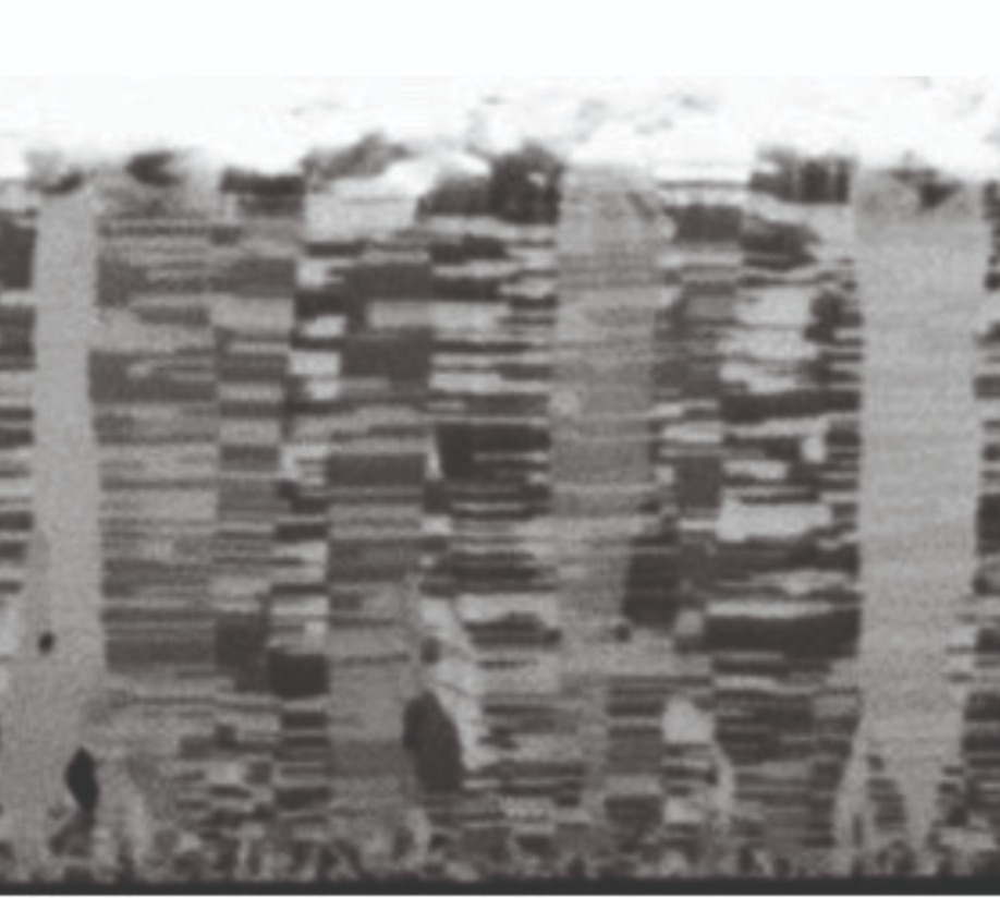
Novafab nano-twin copper, optimal for direct bonding.
To illustrate this point, let’s consider copper plating. For many of today’s manufacturers of devices designed around the pillar/bump process, the extremely advanced 20 μm pitch is unattainable. But this length scale is easy to realise with copper damascene plating. This form of plating has been used for advanced logic interconnects. Although copper plating has recently been displaced by PVD reflow, and in some cases cobalt, at the most advanced nodes, copper plating was the process of record through to the 10 nm node where metal 1 via dimensions reached the scale of around 30 nm or less.

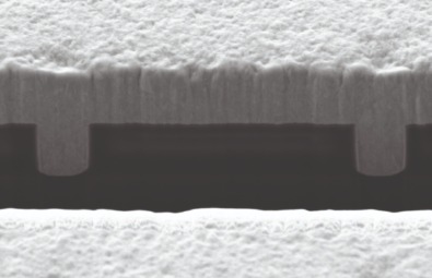
Left: Sub-micron feature filled with gold. Void-free. The aspect ratio is 1.5:1. Right: A magnified image, showing two sub-micron features filled with gold.
When evaluating different options for unit materials, it is essential to consider not only the plating step, but the processes that surround it – and thus consider the pros and cons compared with those associated with pillar integration. Embedded pad plating, often known as feature fill, does require an advanced chemical mechanical polishing (CMP), which precisely planarizes metal and dielectric. Existing copper CMP routinely planarizes feature densities to a level several orders of magnitude higher than that needed for today’s state of the art packaging.
This is not to say that advanced copper CMP is simple, but rather that the necessary development was already driven by advanced interconnect integration and thus already exists. Specific to direct hybrid bonding, the CMP must accommodate the difference in the coefficient of thermal expansion between the dielectric and metal. Complete and reliable bonding demands that the metal bond pads be slightly recessed but precisely so, typically to within 5 nm of specified recess. Thus after the bonding step that unifies the dielectric, the ensuing bonding step for the metal results in an expansion of the two interfacing pads which grow into each other and ultimately form a monolithic interconnect. Again, not trivial, but not a new requirement either.
Copper versus gold
For hybrid bonding, the post-CMP cleaning becomes truly critical. When using copper, there is an established process of record for engineers to draw on. Cleaning chemistries for device metallization have been established that realise excellent particle removal, low residual surface contamination of metal ions and effectively zero metal etching on the exposed features. This is a unit process step that is already established though requires very tight process control.
Our team has shown that by combining proper chemistry formulation with key parameter controls, in our specific case MadDermid Enthone’s MicroFab Au660 sulfite gold electrolyte and our GoldPro reactor, employing specific plating waveform and electrolyte flow profile, an effective and scalable feature fill with gold is readily available today. Working with a key manufacturing partner in an emerging technology, we have developed and demonstrated a gold feature fill of a pad feature with a 1.5:1 aspect ratio. This is a far tighter pitch than that for a pillar/bump involving a 10 μm-wide copper pillar, which is considered to be state of the art for that technology.
The development of gold CMP technology is not as mature as copper CMP, and is subject to a similarly tight process window with regard to metal recess. Of particular challenge is the fact that gold CMP chemistries tend to be considerably more aggressive than those for copper. If aggressive slurries are employed, there are challenges to face in forming a sufficiently smooth dielectric surface while
controlling the recess of the gold features. As with copper, a hybrid bond sequence begins by direct bonding the dielectric surface, followed by bonding of the metal.

Gold plated in multiple crystal orientation using MicroFab Au660 gold sulphite chemistry, supporting optimization for direct bonding
When it comes to optimizing the grain structure for the most efficient bonding, copper metallization has again received more attention than gold. That said, gold has already been shown to be platable in distinctly different orientations, suggesting that there is ample room for near-term optimization.
At some point even gold’s forgiveness to conformal plating and its avoidance of seam lines will give way to the realities of a higher aspect ratio for which conventional gold electrolytes will not suffice. However, since the feature is equivalent to a pad, its current-carrying capacity is defined in the horizontal, not vertical. In other words, the bond pad does not need to be tall to work, so it is unlikely that there will ever be a need to produce a pad with a feature of an excessive aspect ratio. Development may drive towards a ratio of 2:1, with deployment requiring a fill step that more directly resembles true bottom-up plating. Such efforts are already well underway, with significant progress achieved by MacDermid Alpha.
One practical constraint to further development of a more bottom-up gold chemistry technology is the ability to accurately analyse such chemistry. The difficulty stems from being unable to draw on all the conventional electrochemical analysis methods. For copper plating chemistries, which depend on forward and reverse plating – that is, plating and stripping – a rotating disc electrode is used. Gold cannot be readily stripped in a similar way. Fortunately, these challenges could soon disappear, as progress is being made, including novel development by Ancosys GmbH.
Many may wonder why it makes any sense to use gold, rather than copper, given the far higher costs – gold currently commands around $1800 an ounce, compared with just $5 for copper. There are, in fact, two reasons for this move: one is technical, while the other based on the market. Ultimately, chosing gold over copper will impose some trade-offs. Gold CMP, as mentioned, will provide tougher challenges than copper CMP. However, gold potentially opens the process window for steps such as the highly critical post-CMP clean step.
With gold, as with copper, post-CMP cleaning is critical to successful hybrid bonding. With copper, there is the threat of oxidation and the criticality of queue times between steps. It is possible to avoid this and realise a high yield – this is the case in the manufacture of CMOS image sensors – but as scaling continues, requirements around precision recess of the pads are to become more stringent, and there will be an increase in sensitivity to small variation. With gold, as there are no oxidation issues, there is a far wider choice of chemistries for post-CMP cleaning as well as intra-step queue times. Additionally, there is far less concern over: the presence of dissolved oxygen in the chemistry; the exposure to air in a moist environment; and other, related complications.
It is also worth noting that that most compound semiconductor do not move wafers through the fab with overhead transport in a hermetically sealed container. This implication is that there is the threat of environmental variation, which is incredibly costly to address. With gold, the chances are that this is far less of an issue. While you may have to work on your CMP step, you don’t have to rebuild your fab!
From a market perspective, there is obviously a higher cost associated with adding a single layer of gold on the surface. However, the contribution to overall production costs is relatively small. And weighing against this additional expenditure is the wider process window that promises to speed integration with a high yield, crucial to unlocking the door to capturing market share. This can make all the difference between enjoying success in an emerging market and missing out on an opportunity.
Within the semiconductor industry, as technologies advance, they often go out of reach of all but the largest manufacturers. When this happens, new approaches emerge that enable continued innovation, leading to countless technological marvels that enthral consumers. This unfolding of events is behind the development and uptake of hybrid bonding. Whether using conventional copper metallization or gold metallization, this is a process that fabs can adopt, thanks to the availability of commercial tools, such as those we have produced.
- The author would like to thank Dr Robert Rhoades, recognized CMP expert, for his contributions to this article.
A new era beckons, with better devices that draw on the strengths of the entire palette of compound semiconductors
BY RICHARD STEVENSON
Materials tend to be renowned for a particular asset. GaN is widely credited for handling very high power densities, InSb is known for its ability to allow carriers to zip around at high speeds, and HgCdTe is recognise for its capability to detect emission far into the infrared. Yet, for all these materials and more, alongside their strength comes at least one weakness.
Due to this, selecting any material involves compromise, with decisions weighing up what will enable the best overall device performance.
There is clearly much appeal in avoiding this limitation by selecting the optimal combination, rather than picking the best material. But that is far easier said than done, given that there are several tough challenges to overcome when uniting different families of compound semiconductor materials.
While these challenges may initially seem insurmountable, progress is being made, thanks to the toil of many researchers. Due to many different materials and technologies involved in these breakthroughs, it is hard to keep track of all the progress that’s being made. However, thanks to the extensive coverage on this topic at this year’s CS Mantech, held on 25-27 May, all the delegates attending this online meeting could gain a good grasp of the many advances being made to combine markedly different semiconducting materials, and how this success will impact the next generation of devices.
Setting the scene for how far we’ve come already and what the future may hold, Mark Rosker, the director of DARPA’s Microsystems Technology Office, opened the conference by outlining the three different eras for compound semiconductor devices. He views the first wave as that involving the production of devices on native substrates, such as GaAs-based MMICs; and the second as the growth of devices on foreign substrates – examples include GaN-on-SiC HEMTs, as well as antimonide-based structures, grown on GaAs and InP substrates, that form low-power, high-frequency electronic circuits. Rosker argued that a third wave is now starting to emerge, where devices feature abrupt junctions and high-performance materials with dissimilar lattice constants. “The fundamental technology that is being developed may be thought of as junction engineering,” explained Rosker. “Optimisation is happening at the level of the junction, in order to improve the overall device performance.”
To illustrate what a third-wave device might look like, Rosker highlighted a novel HBT pioneered by a collaboration led by researchers at the University of Wisconsin-Madison and Michigan State University. Using transfer of an AlGaAs/GaAs membrane grown on a native substrate, this team constructed a HBT with a diamond substrate, a p-type diamond collector, an Al2O3 intermediary layer and AlGaAs layers that provided the emitter and base junctions (see Figure 1). By employing a grafting technique, the engineers overcame a 37 percent lattice mismatch between the GaAs-based layers and diamond. It’s a breakthrough that unlocks the door to combining some of the traditional merits of a HBT with the excellent heat extraction of diamond, as well as its higher bandgap that boosts the transistor’s breakdown voltage.
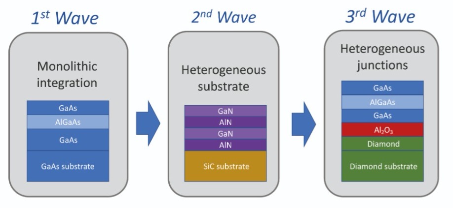
Figure 1. Mark Rosker, director of DARPA’s Microsystems Technology Office, suggests that the compound semiconductor industry will soon enter a third wave of material technology. This era will see devices built from disparate materials.
He also discussed ultra-wide bandgap materials, which he expects to make a significant impact in the next generation of devices. Merits of these materials, such as AlN, Ga2O3, diamond and BN, include a bandgap roughly twice that of GaN and an electric breakdown field that is higher by a factor of about four. However, there are weaknesses with these materials, with some difficult to p-dope and others lacking a substrate.
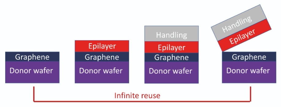
Figure 2. The approach pursued by Jeehwan Kim’s team at MIT enables substrate reuse by inserting a layer of graphene between the substrate (donor wafer) and an epilayer.
To help drive the third wave forward, DARPA has just started a heterogeneous heterostructures programme. In the first phase, the goal is to develop new processes for forming low-defect-density heterogenous heterojunctions.
The second part of the programme is focused on designing novel heterogenous heterostructures, underpinned by accurate physics-based modelling and simulation.
Releasable epilayers
A key process for producing the third wave of compound semiconductor devices is the growth of an epilayer, prior to its transfer to another material. Developing a very promising technology for accomplishing this is a group at MIT led by Jeehwan Kim, who provided an overview of a very broad portfolio of work on this topic to those attending this year’s CS Mantech.

Figure 3. Jeehwan Kim’s team at MIT have used a technique referred to as remote epitaxy to grow a variety of thin films that are separated from the substrate. Apects of this work have been published in the following journals: Nature 544 340 (2017), Nature Materials 17 999 (2018), Nature Materials 18 550 (2019), Nature Electronics 2 439 (2019), Nature Nanotechnology 15 272 (2020), Nature 578 75 (2020)
Two of the most common options for releasing an epilayer are chemical and optical lift-off. The former is not ideal, as chemical treatment may degrade the quality of the substrate, hindering its re-use. “You have to polish your wafer after the release process,” explained Kim, pointing out that etching takes time, and is generally limited to III-V materials. The common alternative, optical lift-off, which involves directing laser emission through the back of transparent substrates to melt away material, also causes damage and takes considerable time – but it is quicker than chemical lift-off.
The novel approach pursued by Kim and his colleagues is to transfer graphene to a donor wafer, before adding an epilayer, applying a handle substrate, and then pulling apart this structure (see Figure 2). Thanks to the weak forces at the interface with graphene, there is a precise release of the epilayers from this carbon structure. Merits of this technique include: a fast release, due to the weak interaction; its application to any material; no need for any post-release treatment; and substrate re-use.
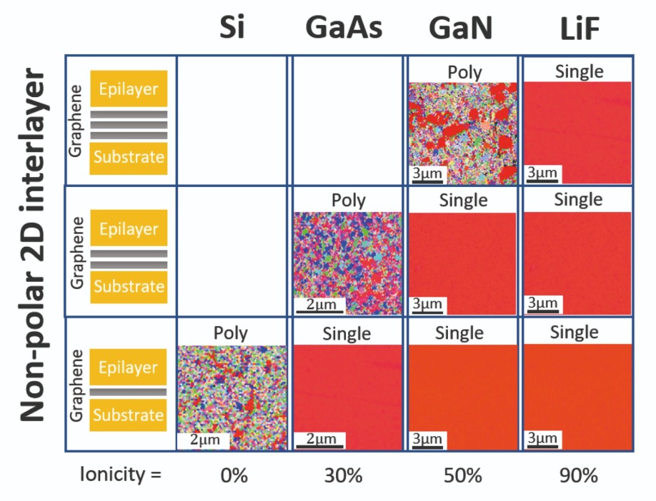
Figure 4. For remote epitaxy, the penetration of the ionic field through graphene is key. For silicon, it’s so weak that subsequent growth produces polycrystalline material. With GaAs, the field is stronger, allowing crystalline growth through a single layer of graphene; and with GaN, the ionic field strength is so high that crystalline material can be formed with a double layer of graphene. More details on this work can be found in Nature Materials 17 999 (2018).
The penetration of the ionic field through the graphene varies with material. With silicon it is weak, causing the growth of polycrystalline material. For GaAs it is a little stronger, so to produce crystalline films by remote epitaxy, graphene must be only a single layer thick; but for GaN, thanks to a relatively strong ionic field, remote epitaxy can yield crystalline films even when using two layers of graphene (see Figure 4).
Kim and co-workers have also investigated heteroepitaxy, growing InGaP that has a lattice-mismatch to GaAs. Due to what Kim describes as spontaneous relaxation on graphene, there is a substantial reduction in dislocation density in the ternary compared with conventional epitaxy.

Figure 5. Working under vacuum, the bombardment of wafers with a fast atom beam (FAB) removes the native oxide, creating a surface for bonding.
While championing all of this opportunity, Kim is open about the challenges, which include compromises in epilayer quality associated with pinholes in graphene, possibly caused by the peeling process. He pointed out that it is important to use the right process to add the graphene layer. For producing compound semiconductor films, a wet process is unsuitable – there are imperfections in the morphology of graphene on its host substrate, such as a lack of perfect flatness, that impair the epilayer. A dry process is better, beginning with the formation of a layer of graphene on SiC.
One of the latest pieces of work by Kim’s team is to use its technology to form an artificial heterostructure containing blue, red and green LEDs. This stack of LEDs, which have lateral dimensions of several microns, is a promising candidate for making displays based on microLEDs.
Bonding wafers
A more established approach for bringing dissimilar compound semiconductor materials together is direct-wafer bonding. A variant of this, known as surface-activated bonding, has much appeal because it does not require any wet processing, with wafers bonded together at room temperature.
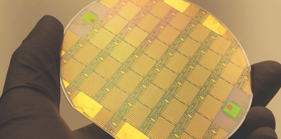
Akash, the pioneer of GaN-on-diamond, is producing 100 mm wafers in volume.
At this year’s CS Mantech, Naoteru Shigekawa, who is a group leader at Osaka City University and an expert in this form of wafer bonding, outlined the criteria for optimising this process, before illustrating its capability with examples of novel devices. While his facility is limited to bonding wafers up to 2 inches in diameter, he is quick to point out that there are commercial tools available, suited to high-throughput bonding of 300 mm wafers.
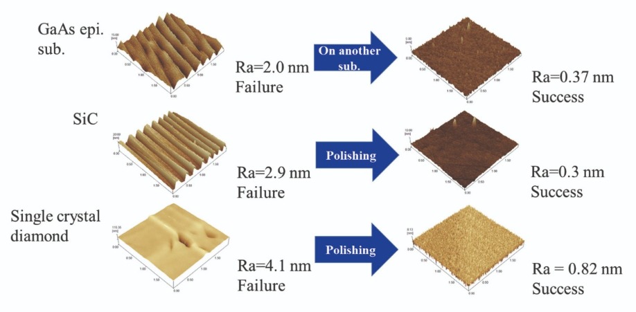
Figure 6. The flatness of the wafers governs the bonding yield. Polishing reduces roughness, and increases the chances of a high-quality bond.
Care is needed when applying this form of bonding, because surface activation leads to dry etching, which can increase surface roughness and impair yield. Another downside of etching is that it introduces mid-gap states. “We assume that such mid-gap states have a negative impact on electrical properties of bonding interfaces,” stated Shigekawa, who added that one solution is post-bonding annealing, which can lead to the recovery of interface characteristics.
Illustrating this point, Shigekawa showed transmission electron microscopy of bonded silicon and GaAs wafers. Prior to annealing, there is an amorphous-like transition layer at the interface. Annealing at 300 °C causes this layer to shrink, and at 400 °C it disappears, thanks to recrystallisation.
Shigekawa and colleagues have also used electrical measurements to assess how annealing adjusts interfacial properties. Investigations of junctions formed by bonding two n-type silicon wafers together, and also by bonding two p-type silicon wafers together, showed that annealing at 1000 °C for 10 minutes drives down the density of interface states from around 1013 cm-2 eV-1 to one-fifth of this value.
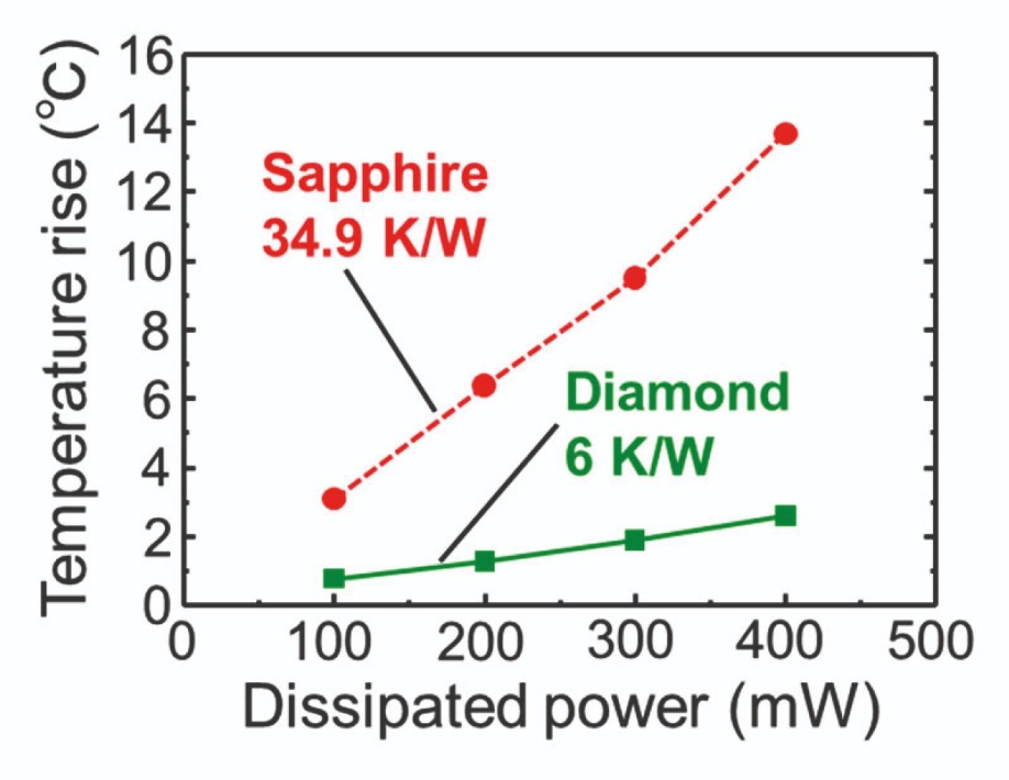
Figure 7. Compared to sapphire, diamond has a tremendously high thermal conductivity that drives down thermal resistance at this junction.
Using a thermal imager, Shigekawa and co-workers have measured the thermal resistance of their junctions. To provide a benchmark, they used a bonded GaAs-sapphire junction, which had a thermal resistance of 35 K/W (see Figure 7). In comparison, the GaAs-diamond junction has a resistance of just 6 K/W. This vastly superior value allows devices to be driven harder without overheating, or the adoption of simpler approaches to thermal management.
The researchers have also considered junctions formed by bonding GaN to diamond. Micro-Raman measurements on these structures, undertaken by Martin Kuball’s team at the University of Bristol, revealed that the stress within these structures is similar to that of GaN-on-silicon.
Diamond dissipation
At Akash Systems of San Francisco, CA, much effort has been devoted to developing GaN-on-diamond transistors, power amplifiers and radios for satellite communication. In this environment, the only mechanism for dissipating heat is radiation. With GaN-on-diamond, heat is drawn out of the channel of the HEMT far faster than with GaN-on-SiC, permitting a higher substrate temperature – and ultimately better heat extraction via radiation.

Table 1. engineers at Akash have many reasons for adopting a glass frit process when producing their GaN-on-diamond devices.
Those attending CS Mantech gained insights into the development of Akash’s GaN-on-diamond technology in a presentation by the company’s Vice President of Materials, Daniel Francis. He explained that many of the technical team are former founders and employees of Group4 Labs, which pioneered the technology. Progress in GaN-on-diamond continued after the acquisition by Element Six, and also after the launch of Akash, which bought-out the IP and introduced a production process on 100 mm wafers.
At Akash, engineers form devices by taking unprocessed GaN-on-silicon epiwafers, bonding a carrier to the epi-side, removing the substrate, growing a layer of diamond in its place, and then removing the temporary carrier. As the diamond that’s deposited forms a rather rough layer, this has to be polished.
Options for attaching the carrier to the epiwafer include diffusion bonding and plasma-activated bonding. But at Akash they prefer glass frit bonding – also known as glass soldering – for several reasons (see Table 1). The primary attributes of frit bonding are that it can be applied to a full wafer, it maintains its strength at the high temperatures subsequently employed for diamond growth, and it accommodates bow, warp and defects in the GaN.
Francis explained that by melting glass, they can cater for surface roughness and bow. “Because you make the glass thick enough, you can accommodate some level of roughness for defects that are five microns, without too much trouble.”
Working in partnership with Kuball’s team at Bristol University, the team at Akash have quantified the improvements in heat extraction that come from removing transition layers. These transition layers are hampered by their ternary nature, and also by the numerous defects (see Figure 8). Thermal conductivity is typically 15 W m-1 K-1, a value about ten times lower than that for GaN. To avoid this issue, Akash removes these transition layers, before adding diamond, which has a thermal conductivity of 1600 W m-1 K-1.
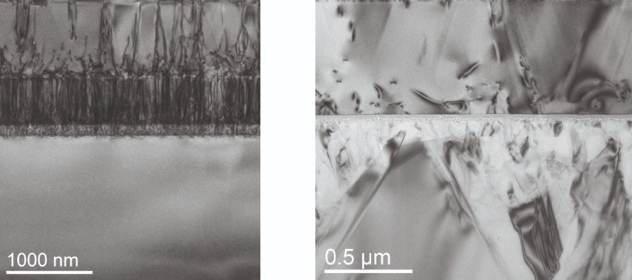
Figure 8. Akash uses GaN-on-silicon HEMTs as the starting point for the production of its GAN-on-diamond devices. Transmission electron microscopy images of GaN-on-silicon, showing a very high defect density in the transition layers (left), and GaN-on-diamond (right).
As the deposited diamond forms grain that are tens of microns in size, polishing processes are needed to ensure a smooth surface. A first step reduces peak-to-valley variation from 30 μm to 5 μm, before a second step takes the surface roughness down to 0.5 μm . Applying both of these steps trims the total thickness of the diamond, which falls from around 200 μm to 105 μm.
Francis and co-workers have compared the performance of GaN-on-SiC HEMTs with those based on GaN-on-diamond. Measurements on the former, devices with a 150 nm gate length that operate at a frequency of 20 GHz and an efficiency of 25 percent, have a base plate temperature of 25 °C when the channel temperature is 200 °C. For the GaN-on-diamond variant, because the team is yet to perfect the 150 nm process, a gate length of 250 nm is employed. The larger gate drags down efficiency to 20 percent. However, encouragingly, the base plate temperature can be as high as 100 °C for a 200 °C channel temperature, allowing the device to operate up in space without the need for active cooling.
This promising result, like those of the devices described by Rosker – and those made at MIT and Osaka City University – provides a glimpse into the future of what will be possible. When devices draw on disparate materials, many doors could open, helping to elevate the importance of our industry to an entirely new level.
Forming a gate oxide without oxidation smashes through a barrier that has held back the SiC MOSFET for 20 years
BY TSUNENOBU KIMOTO AND KEITA TACHIKI FROM KYOTO UNIVERSITY
GOVERNMENTS FROM ALL AROUND WORLD are now preparing for this year’s UN Climate Change Conference, widely referred to as COP26. At this gathering, which is due to take place in early November in the UK, all nations in attendance will be asked to offer a commitment to cutting their carbon footprint.
The level of ambition they can promise will be governed by their plans for installing renewable forms of energy. But another factor that they ought to consider is how efficient they are in using the energy they generate, and whether they can make gains on this front. In almost all kinds of electric and electronic system, the efficiency of power conversion, such as AC/DC and DC/AC conversion, ranges from 85 percent and 95 percent. That implies that with current technology, about 10 percent of electric power is wasted, in the form of heat. That’s a significant proportion: just imagine how many gigawatts of electric power is wasted in countless systems by power conversion, or how many coal-fired power stations could be mothballed by making gains in efficiency.
Most of this power loss is attributed to Joule heating inside power semiconductor devices, which are almost exclusively made from silicon. Power devices made from this semiconducting material have been playing key roles in electrical products and infrastructure for many decades, but this technology is now highly mature, offering little opportunity for further improvement.
However, significant gains are possible by switching to wide bandgap semiconductors, such as SiC, GaN, and Ga2O3. Interest in all three has been rocketing in recent years.
One striking property shared by all these wide bandgap semiconductors is a very high critical electric field strength – it is more than ten times that for silicon. Differentiating the three from one from another are some unique features: SiC is renowned for its wide range of doping control, GaN is blessed with a AlGaN/GaN heterostructure that creates a high-mobility channel, and Ga2O3 has the merit of melt growth of bulk crystals.
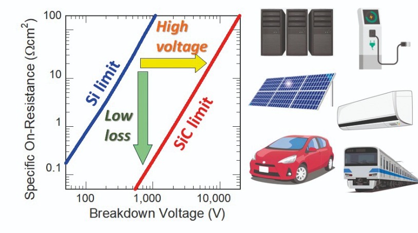
Figure 1. (left) Unipolar limits of silicon and SiC power devices, showing the trade-off between the on-resistance and breakdown voltage. (right) Typical application areas for SiC power devices (MOSFETs and Schottky barrier diodes).
As chipmakers draw on all these attributes, sales of SiC power devices are on the rise. SiC Schottky barrier diodes and power MOSFETs specified at voltages from 600 V and 1700 V hit the market in 2001 and 2010, respectively, and sales have been ramping since 2015. Driving increases in shipments is the adoption of SiC power devices in servers and workstations, photovoltaic inverters, air-conditioners, fast chargers, railcars, and the electric vehicles of Tesla and Honda. In all these applications SiC provides substantial energy savings (see Figure 1). Sales of SiC devices are tipped to continue on this impressive trajectory, due to the tremendous expansion in the manufacture of electric vehicles, as well as huge investments in SiC material and devices underway in the US, Europe, Japan, and China.
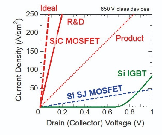
Figure 2. The relationship between on-state current density and voltage for the 650 V-class SiC MOSFET, silicon super-junction (SJ) MOSFET and silicon insulated gate bipolar transistor (IGBT). For the SiC MOSFET, values are provided for the latest products, R&D device, and the ideal device.
The weaknesses of the SiC power MOSFET are highlighted by considering contributions to this device’s on-resistance (see Figure 3). In any class of power MOSFET, on-resistance is a combination of several factors, including drift-layer resistance, channel resistance, substrate resistance, and contact resistance. For the 600 V SiC power MOSFET, drift-layer resistance is so low that other contributions to resistance cannot be ignored. Compared to an equivalent silicon device, the drift-layer resistance of the SiC MOSFET is almost 300 times lower, while its channel resistance is about 30 times higher, due to poor channel mobility. This hike in channel resistance is incredibly detrimental, obliterating much of the benefit of a SiC power MOSFET over its silicon rival. For 600 V and 1200 V SiC MOSFETs, channel resistance accounts for about 70 percent and 50 percent of the total on-resistance, respectively.
A decades-old problem
An obvious question to ask is this: Why is the channel resistance of the SiC MOSFET so high? The reason is that at the interface between SiO2 and SiC there is an extremely high density of interface states, also known as traps. While silicon enjoys a density of interface states below 1010 cm-2 eV-1, for SiC this exceeds 1012 cm-2 eV-1. This high value has been holding back the performance of SiC devices since 1990. It is to blame for a channel mobility of no more than 40 cm2 V-1 s-1, despite a bulk electron mobility of around 1000 cm2 V-1 s-1. In fact, in SiC power MOSFETs where the p-body is relatively heavily doped, the channel mobility is even lower – typically, it’s 15–25 cm2 V-1 s-1, so just a few percent of the value for bulk mobility.
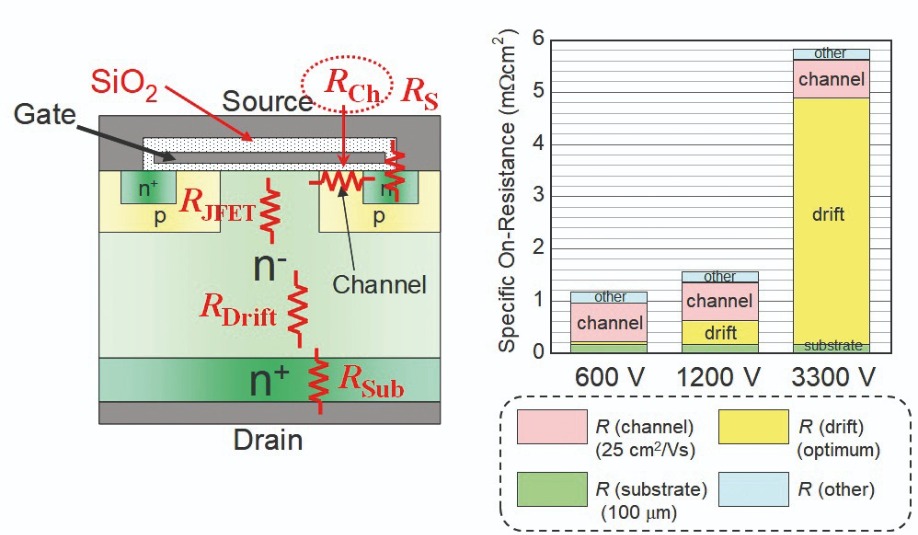
Figure 3. (left) Schematic cross-section of a vertical power MOSFET and its major resistance components. (right) Major contributors to the on-resistance of 600 V, 1200 V, and 3300 V SiC power MOSFETs. The on-resistances of 600 V and 1200 V SiC MOSFETs are severely limited by the channel resistance.
Since the start of this century there have been numerous investigations and unique trials all over the world to try and improve the performance of the SiC MOSFET. Highlights from the last 20 years are sodium-enhanced oxidation developed at Philips, and annealing in a POCl3 ambient, pioneered by engineers at NAIST. Both techniques resulted in high channel mobilities, typically 90-160 cm2 V-1 s-1, but the approaches are unsuitable, introducing a threshold-voltage instability and a short oxide lifetime at a high electric field.
Oxidation-free oxide formation
Our team at Kyoto University, Japan, has devoted many years to basic studies of the SiC MOS structure, and to also developing a novel technology for improving the MOSFET. Given that an interface state density over 1012 cm-2 eV-1 is somewhat abnormal, this suggests that something must be wrong with the SiO2/SiC system. To uncover the cause, we have asked ourselves this simple question: What happens with carbon atoms in SiC when SiC is thermally oxidized? Almost all carbon atoms are removed during oxidation of SiC to form CO molecules. But not all – some remain near the interface, and are the main cause of defect formation.
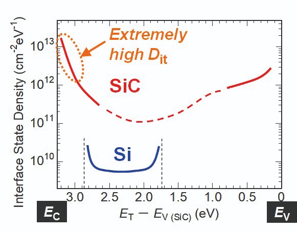
Figure 4.Energy distributions of the interface state density for SiC and silicon MOS structures. The extremely high defect density near the conduction band edge (Ec) in SiC is the main cause for the low mobility of n-channel MOSFETs.
Offering further insight into the oxidation process are a number of first-principles calculations on the SiO2/SiC interface. These theoretical investigations show that some C-C defects have low formation energies and can create electrically active levels near the conduction band edge of SiC.
After considering all these experimental findings and theoretical studies, we conceived the idea that it is crucial to avoid oxidation of SiC as much as possible when forming the gate oxide during MOSFET fabrication, because a high density of defects is inevitably generated by SiC oxidation. While the SiC community is happy to continue to use thermal oxidation of SiC to form SiO2, our view is that much could be gained by taking the time to develop another approach to producing high-performance SiC MOSFETs. Our solution, which we will now detail, is to use a three-step process for forming a high-quality SiC MOS interface (this is summarised in Figures 5 and 6).
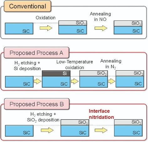
Figure 5. Flows for the conventional oxide formation process and two original processes (Process A and Process B) developed at Kyoto University. In the original processes, the oxide is formed by three steps; H2 etching, oxide formation without SiC oxidation, and interface nitridation.
Note that at no point do we employ sacrificial oxidation of SiC, which is thermal oxidation followed by oxide removal. Those that do use sacrificial oxidation, either prior to MOSFET fabrication or after epitaxial growth, are in danger of creating very defective regions on the surface of the SiC wafers.
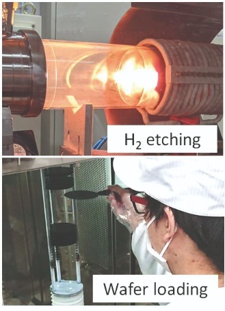
Figure 6. High-temperature hydrogen etching and wafer loading for interface nitridation to form high-quality SiO2/SiC structures.
A handful of groups have also tried to deposit silicon, before converting this to SiO2 by thermal oxidation. This is not successful: the temperature for conversion from silicon to SiO2 is too high, and oxidation of the SiC surface results, driving the generation of a high density of defects.
During our studies, we have looked in detail at the impact of all three steps of our process. We have found out that all of them are mandatory for realising a very low interface state density near the conduction band edge.
Depositing SiO2
In this remainder of this article, we detail the SiO2 deposition process (Process B), which has the merit of technological simplicity. We compare this approach with conventional thermal oxidation and nitridation annealing, in either N2 or NO (see Table 1).
Measurements of the energy distributions of the interface state density for these four different processes underscore the promise of our original processes (see Figure 7, which demonstrates the superiority of process B, for both H2-CVD-NO and H2-CVD-N2 processes). With Process B, the defect density at an energy 0.2 eV below the conduction band edge is about three-to-five times lower than it is for the conventional process used for manufacturing SiC power MOSFETs, based on oxidation and nitridation with NO. When the MOS is produced with the conventional process, the interface state density exhibits a rapid increase toward the band edge; with our original process energy distributions of the interface state density are rather flat, indicating a different nature of interface defects.
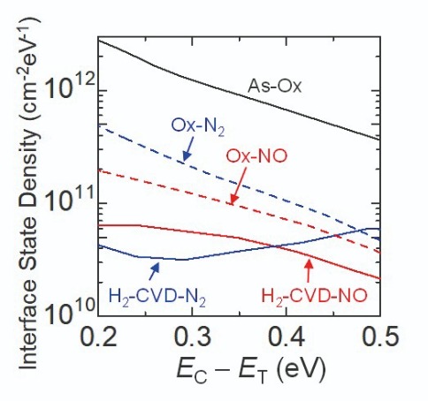
Figure 7. Energy distributions of the interface state density for SiC MOS structures with oxides formed by five different processes: as-oxidized (As-Ox); conventional oxidation and subsequent nitridation (Ox-NO and Ox-N2); and the two novel technologies developed at Kyoto University (H2-CVD-NO and H2-CVD-N2). The new processes yield a very low interface state density of typically just 5 x 1010 cm-2eV-1 near the conduction band edge.

Table 1. Four different processes for gate oxide formation. H2-CVD-NO and H2-CVD-N2 are pioneered by Kyoto University, while Ox-NO and Ox-N2 are conventional.
Development of the SiC power MOSFET has witnessed several false dawns. Processes showing initial promise by delivering low defect densities or high channel mobilities have fallen at the next hurdle, due to either a poor dielectric breakdown characteristic of the oxide or a large threshold voltage instability induced by the gate bias.
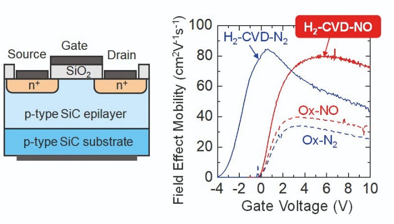
Figure 8. (left) Schematic cross-section of a fabricated n-channel SiC MOSFET. (right) Mobility versus gate voltage for SiC MOSFETs with gate oxides formed with four different processes. The H2-CVD-NO MOSFET exhibits more than twice the mobility of the conventional MOSFET at a high gate voltage and normally-off operation.
One of our next goals is to apply our technology to non-basal planes. It is well known that SiC MOSFETs reach a higher level of performance when MOS channels are formed on non-basal planes ((1100) or (1120) face). In these devices, known as trench MOSFETs, channel mobilities of over 100 cm2 V-1 s-1 have been attained with the conventional process. Switching to our process should yield even higher values. Several SiC device manufacturers have shown much interest in this possibility, got in contact with us, and technology transfer has started.
A higher mobility is a major asset for a SiC power MOSFET. It delivers a substantial reduction in the specific on-resistance in 600 V to 1200 V devices, assuming a doubling or tripling of channel mobility. The smarter move by chipmakers, however, is to trim chip size while maintaining on-resistance. Halving the chip size would double the number of MOSFET die obtained from one wafer, and also drive production yield towards 100 percent, thanks to reductions in the probability of meeting a device-killing defect or a pattern failure. All these factors will help to reduce the cost of SiC power MOSFETs, and in turn accelerate the shipment of these devices.
While we have made much progress, one fundamental question remains: what is the origin of interface defects in SiC MOS structures? As we are now able to fabricate SiC MOS structures with a very low defect density, we can expect that physical and chemical analyses of the high-quality interface, as well as poor-quality samples, should provide useful insights into the cause of defects.
In addition to looking into this matter, we plan to further improve our original processes. We have realized that variations in the annealing conditions after oxide formation in the proposed processes have a striking impact on interface quality, which is not the case with conventional technology. This is further evidence that the development of the SiC MOS has just entered an exciting new era, after decades of stagnation.
The authors would like to acknowledge T. Kobayashi and M. Kaneko from Kyoto University for their contribution to this study.
K. Tachiki et al. Appl. Phys. Express 14 031001 (2021)
K. Tachiki et al. Appl. Phys. Express 13 121002 (2020)
T. Kobayashi et al. Appl. Phys. Express 13 091003 (2020)
T. Kimoto et al. Appl. Phys. Express 13 120101 (2020)
T. Kobayashi et al. J. Appl. Phys. 126 145302 (2019)
G. Chung et al. IEEE Electron Device Lett. 22 176 (2001)
By emulating photonic neurons, circuits built from memristor lasers can form computers that mimic the brain
BY BASSEM TOSSOUN FROM HEWLETT PACKARD LABS
IN 1936, ENGLISH mathematician and computer scientist Alan Turning wrote a paper entitled, On Computable Numbers. In this work he proposed a computing system, named the Universal Turing Machine, that is design to solve specific mathematical problems programmed into it. The underlying principle behind Turing’s design is that instructions, stored on a tape, are executed to compute and solve complex mathematical problems. In 1941 Turing’s design became a reality, when he led a team that built an actual computer used to decode encrypted messages from Nazi Germany. This Turing Machine played a major role in supporting Britain and its allies in the Second World War; it is thought to have shortened the conflict by two-to-four years.
A few years after the war had ended, a brilliant Hungarian mathematician by the name of John von Neumann built on Turing’s work, outlining the modern-day computer architecture in the monumental text, First Draft of a Report on the EDVAC. The computer structural design that he championed has taken his name, being commonly known as the von Neumann architecture. At its heart is a central processing unit: it swaps data stored within memory; computes on the data using an arithmetic logic unit; and then sends this back to the memory, to be stored as memory registers. The revolutionary work of von Neumann’s jumpstarted the computing revolution, laying down the foundational structure for nearly all of today’s computers.
Another milestone in computer development came in 1959, when two engineers working at Bell Labs – Mohamed Atalla and Dawon Kahng – invented the MOSFET, one of the most fundamental building blocks in modern electronics. This class of transistor is integral to the computing revolution because it makes it practically viable to integrate electronics into densely packed integrated circuits on silicon. Note that Atalla also played a key role in developing the compound semiconductor industry. In 1966 he co-founded the Hewlett Packard (HP) Labs. This has been a hub of innovation in computing, and also in semiconductor electronic and photonic devices, including LEDs, Schottky diodes and power transistors, made from the likes of GaAs and InAs.

A schematic diagram of a TiO2/TiO2-x memristor discovered by HP Labs.
The marvellous memristor
Just a little over a decade ago, a team of researchers at HP Labs, led by Stanley Williams, made a monumental discovery: the first experimental demonstration of a device known as a memristor. This class of memory device completes the quartet of fundamental components, the other three being the resistor, the capacitor and the inductor. Williams and co-workers fabricated this device by sandwiching two thin layers of oxide materials between a pair of platinum wires. By ramping up the voltage supplied to this simple structure, the researchers caused oxygen atoms to ionize and migrate, effectively changing the resistance of the material. Thanks to this, the device is able to store memory within itself as resistance.

A cross-section schematic diagram and transmission electron microscope (TEM) image of the memristor laser.
The invention of the memristor spawned much interest in university research groups and government and industrial research labs, and has led to the generation of myriad patents and publications. Highlights include the development of memristor cross-bar arrays, which emulate artificial neurons and synapses in a neural network for low-energy, high-density computing and memory storage. However, despite research progressing at breakneck speed, the memristor is yet to deliver the bang it’s expected to make in industry. There are various challenges related to production, such as difficulties in producing a high volume of memristors with a high yield, uniform performance from device to device, repeatability and long retention times.
In the meantime, Hewlett Packard Labs has been developing devices based on silicon photonics, a revolutionary technology that helps to circumvent the von Neumann bottleneck. This technology, which involves the integration of photonics on robust, cost-effective silicon, has the potential to bring photonics closer to where data is electronically stored and generated by CMOS electronics.
Silicon photonics offers an alternative to traditional electrical interconnects made from copper or aluminium – they suffer from physical limitations, such as crosstalk, as well as signal propagation delay and attenuation at high data-transmission rates. Moving to the photonic domain of optical fibres and waveguides addresses much of this, while speeding data delivery. Compared with electrical interconnects, which can only carry one channel of data at a time, waveguides accommodate multiple wavelengths. At the other end of the waveguide, data that has been encoded at each wavelength is converted into electrical signals, which are processed and stored. The great attraction of silicon photonics is that it offers a platform for producing low-cost, high-bandwidth, energy-efficient optical interconnects that facilitate the transfer of vast amounts of data from chip-to-chip and even on chip within a supercomputer.

The current-voltage characteristic of the memristor integrated within the memristor laser. A hysteresis loop, the fingerprint of a memristor, was measured.
high-bandwidth, energy-efficient optical interconnects for future high-performance computers and data centres. And within Hewlett Packard Labs, the Large-Scale Integrated Photonics group, of which I am a part, has devoted much time to research on this technology. Our group has demonstrated an extensive portfolio of devices and components based on silicon photonics, including high-speed modulators, photodetectors and lasers.
Adding a laser
A trademark device developed within our group is the silicon microring resonator. It consists of a ring waveguide with a carefully chosen diameter, etched onto silicon and designed to filter out light of a specific wavelength.
By bonding compound semiconductor lasers directly to the silicon microring resonators, our team has fabricated hybrid silicon microring lasers. These compact devices are ideal for digital data transmission within a coherent optical communications system.
One of us at HPE, research scientist Di Liang, trailblazed a new device by following in the footsteps of Mohamed Atalla’s invention of the MOSFET. Fifty years on, Liang took the MOS capacitor that revolutionized the world of electronics and integrated it with a laser. The result is the world’s first III-V-on-silicon MOS microring laser, which has the MOS capacitor integrated into the cavity of a laser diode to fine tune the output wavelength of the light generated.

John von Neumann, inventor of the EDVAC, one of the first built computers in history.
Within this microring laser, the area of the capacitor overlaps the optical waveguide. This leads to changes in the accumulation of charges on each side of the capacitor and within the waveguide, and gives rise to a phenomena called the plasma dispersion effect. It is an effect that is related to the density of free carriers in a material, and how this changes the material’s real and imaginary refractive index.
One of the impacts of plasma dispersion is a shift in both the wavelength of light resonating inside the microring, and the output wavelength of the laser. Using this laser, Liang and co-workers demonstrated data transmission at 15 Gbit/s, at an energy rate of just 1.2 pJ/bit. These numbers underscore the capability of the III-V-on-silicon MOS microring laser for providing an energy- and cost-efficient light source for high-speed interconnects within supercomputers.
More recently, I have spearheaded a new effort within the group, taking the microring laser we have developed and combining it with another revolutionary device discovered at HPE Labs, the memristor. Motivation for this effort is the wonder of whether the integration of a memristor with a microring laser could create a device that stores data within the laser.
To test out this idea, our team began by investigating whether the MOS capacitor within this hybrid device could produce a hysteresis curve in its current-voltage characteristics. Our results were very encouraging, finding that this device indeed acts as a memristor. This was a great surprise, since we had been making these devices in the lab for years, and were unaware of this behaviour. Only now did we appreciate their significance as it lead to the world’s first memristor laser – that is, the first tuneable laser with non-volatile optical memory.
We found that when we apply a high enough electric field across the memristor, the MOS capacitor no longer behaves as a capacitor, but rather as a resistor. The change in characteristics comes from an electroforming process inside the oxide material, with a high electric field pushing oxygen atoms out of their original location and driving them in a certain direction. In their wake is a conductive path for current to flow. What has ultimately happened is a change in the conductivity of the oxide material.

Memristor laser output power as a function of wavelength at its original state, and when the memristor is switched on and off.
When our device operates in its low resistance state, conductive filaments are formed, creating localized paths for current to flow throughout the oxide material. These filaments cause the resistance of the oxide to fall by at least two orders of magnitude, driving a hike in current density by a similar factor. When this happens, Joule heating occurs through the conductive filaments within the memristor. This heating dominates the plasma dispersion effect, and leads to a shift in the refractive index that produces a redshift in the laser wavelength.

Measured laser output power as a function of wavelength after setting the memristor on and resetting it back off.
To verify this modus operandi, we have used a cleaved fibre to measure our device, and to also couple light from the memristor laser into a grating coupler and then on to an optical spectrum analyser. Recording the optical spectrum at 0 V after the device is turned on and off revealed that there is an abrupt change in the optical wavelength after setting the memristor on, but no change in the optical wavelength after resetting the memristor back off. As the switch in states occurs in roughly 75 ns, our device has the potential to provide high-speed data storage.
One of merits of this device is that it is already compatible with our group’s silicon photonics platform. This allows the formation of memristors without any additional cost, material, or design complexity. By realising close integration of memory and photonics on the same chip, we are enabling computing on the edge. For instance, our group is currently fabricating a photonic memory circuit to produce an optically accessible memory chip with ultrafast read times. This circuit offers great versatility – it can be used on the front-end of a device to not only communicate data to the cloud at high-speeds, but also store and process data within the same device. Having the data stored and processed closer to the device interface reduces the overhead latency in going back to the cloud to retrieve data. What’s more, this approach can tackle increases in power consumption in a computing system that come from the slow process associated with optical-to-electrical conversion between photonic integrated circuits and memory chips. By keeping some memory on the same chip as the photonics, we save a great deal of energy.
Mimicking the brain
We are also designing a circuit that uses memristor lasers to emulate photonic neurons. The plan is to use our optoelectronic platform to construct a neuromorphic computer, which is a computing systems inspired by the human brain, essentially the most efficient computer in existence. A human brain consumes less than 20 W of power to process an exaflop – that is one quintillion floating point operations per second. Along with our peers, we have a lot to learn about the operation of the human brain and how we can adapt our modern computer architectures to mimic them.
Applications for neuromorphic computing include machine learning and image recognition. For instance, if a specific program has been already trained within a neuromorphic circuit to complete a certain kind of task, this program can be used without needing to recompute an instruction set from scratch each time it is executed. This is similar to exercising neural pathways in the brain for certain tasks, such as playing a guitar. Each time a proficient guitarist picks up this instrument, they don’t have to learn how to play it from scratch. Instead, they draw on muscle memory. Being able to do so provides large savings in time and energy when performing certain tasks for specific applications.
Studies have shown that the brain is a massive organ, with an interconnected network of neurons communicating with each other asynchronously and in parallel. Consequently, there is no clock that each neuron needs to sync with, and one neuron can communicate with multiple neurons at the same time.
This is a different working arrangement from the traditional von Neumann computer, which executes instructions and computes data sequentially at a specific clock frequency. Our hope is that by integrating photonics side-by-side with memristor-based neuromorphic electronic circuits, data can distributed within a neural network in a massively parallelized way using wavelength-division multiplexing communication links.
By adopting this architecture, neurons, represented by memristors, will communicate with multiple other neurons at the same time, using an array of memristor lasers. Within this configuration, data will be routed through an integrated optical waveguide, like an axon (also known as a nerve fibre) that carries signals at high speed and low energy.
To form neural pathways, we will add synaptic weights of neurons together, before storing the computed results on memristor lasers. When the weight of a neuron adds up to a threshold, an action potential will occur, triggering the memristor laser to send out a spiking signal, in the form of a switch in the output lasing wavelength.
By developing this technology, our team, and colleagues of ours at Hewlett Packard Labs, have equipped ourselves with the IP and know-how to integrate storage, compute, and high-speed optical interconnects on the same chip.
This milestone provides us with the essential tools for rearchitecting the computer and enhancing the brute power of future supercomputers. While it is yet to be fully mapped out exactly how exactly this technology will be applied, there is sure to be exciting shifts and advancements in computing when this technology develops a few years from now.
Surging sales of wearable devices will drive a new era for the IC, with planar FETs replaced with vertical gate-all-around transistors
BY KATSUHIRO TOMIOKA FROM HOKKAIDO UNIVERSITY
WHEN COMMERCIALIZATION of the IC began back in the 1960s microprocessors would feature a dozen or so transistors, each with dimensions of tens of microns. In the intervening years we’ve come an awfully long way. Progressing at rates described by Moore’s Law and Dennard Scaling, we have been on an exponential trajectory. While its not been easy at times, requiring the likes of the introduction of a high-k gate oxide, metal gates, strained silicon and multi-gate architectures to keep up the pace, continued advances have ensured that the world’s leading fabs are now churning out ICs with 50 billion FETs. The big question is this: given the exceptional miniaturization of the FET, how will researchers extend LSI from now on?
While these researchers ponder this, they must consider how the pandemic has changed the way we use electronic devices, and how electronics are developed. We now live in a world where there are fewer physical spaces and cyber spaces are on the rise. This has meant that working remotely is now the norm in many sectors, and socialising on-line is commonplace. There is also more interest in wearable augmented-reality devices. The likes of smart glasses, earphones, wrist bands and rings, previously thought of as gadgets of the distant future, are now the technologies we want to soon inhabit our world.
Getting there requires addressing concerns over wearable devices. Compared to smartphones and other forms of portable electronics, they have limited functionality. It also challenging to make them small enough, so that they are not cumbersome. Success on both fronts demands a new generation of high-performance LSIs to serve in a post-5G era.
Our team at Hokkaido University, Japan, is tackling this challenge by developing a number of promising technologies. We have considered performance per unit volume, finding that when the system performance is represented by memory bytes, this plummets with the miniaturization of the device size (see Table 1). Due to this trend, we are convinced that wearable devices of the post-5G era need to contain a high-performance computing system.
What will the transistor technology look like in such a system? Consequences of miniaturisation indicate that it can’t be based on planar integration, the mainstream architecture since the 1960s. We can also rule out the stacking of LSI chips – the so-called 3D integration or chiplets – due to serious thermal management problems. So a new integration schemes is needed, delivering much denser devices in a smaller footprint than modern LSI. This approach demands alternative switches, used to create small, high-performance architectures with ultra-low thermal dissipation.
Four ways forward
We are investigating four different approaches for producing modern FETs that could fulfil these requirements: an alternative FET structure, different channel materials, a new switching mechanism and a refined integration scheme (all are outlined in Figure 1).
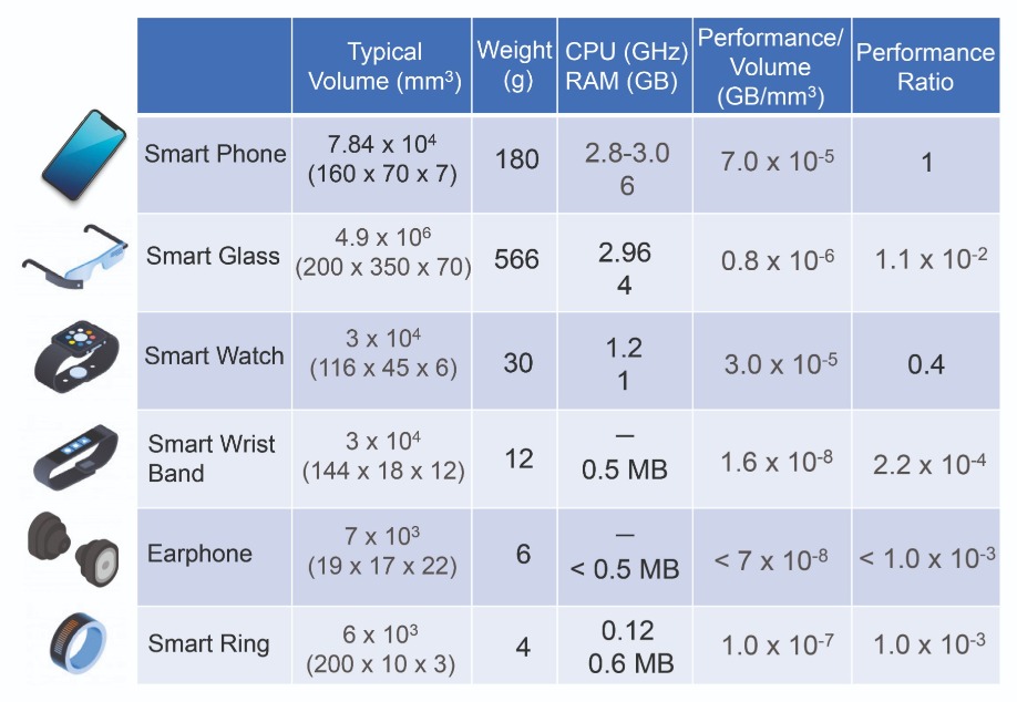
Table 1. Comparison of conventional wearable devices. The device performance and functionality refers to values of RAM memory. Performance per volume rapidly decreases. The performance ratio is the fraction of the performance per volume compared with that of a smartphone.
An option for decreasing the off-state leakage current is to shift to a gate-all-around architecture. With this design, the gate metal wraps all around the channel to provide the best electrostatic control of the gate.
When it comes to replacing the channel material, there are several strong candidates for taking the place of silicon. Contenders include III-Vs, germanium, and two-dimensional transition-metal dichalcogenides. All promise to provide a high on-state current under low bias, thanks to their high carrier mobility and low electron/hole effective mass. However, the latter is actually a mixed blessing, as the small effective mass also results in a high tunnelling leakage current. So, when these alternatives to silicon are deployed in a multi-gate architecture, efforts must be directed at driving down the leakage current.
Another issue that can arise when using higher mobility materials is that there is an inherent mobility mismatch between the n- and p-channels – this is a problem in CMOS architectures. It may not seem a big issue, given that designers of LSI can adjust the device area to ensure current matching between n-channel and p-channel FETs. However, this is not possible when there is an extreme mobility difference, such as that found in some III-V/germanium materials. In these cases, more success might result from expanding the device area out of the plane, since faster channels are restricted to the vertical gate-all-around architecture.
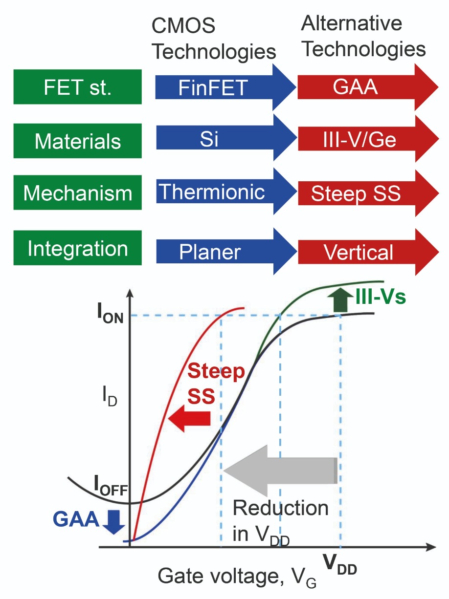
Figure 1. There are alternative technologies for conventional CMOS; FET structures, channel materials, switching mechanisms, and integration schemes. Included is an illustration of switching curves by introducing alternative technologies.
Fortunately, there is a way to overcome this limitation. What’s needed is to switch to a device that operates on non-thermionic processes, as they are not governed by the Boltzmann distribution of carriers. Operation of such devices may be based on quantum tunnelling, impact ionization, negative-capacitance, or mechanical vibrations. With any of these switching mechanisms the sub-threshold slope can be far steeper than 60 mV/decade.
A history lesson
Back in the late 1980s, Japanese engineer Fujio Masouka and his co-workers, working at Toshiba, invented the first vertical gate-all-around FET. Masouka, incidentally also the inventor of NAND flash memory, referred to this device as the surrounding-gate transistor. Whatever its name, it is a device that that will change the integration paradigm. Right now, all electronics devices used in our daily lives are based on the electronics of the 1960s. While deviating from this is certainly challenging, it has to happen, with a shift to the designs shown in Table 1. It is a change that is certainly feasible, since flash memory already uses a type of vertical gate-all-around architecture.
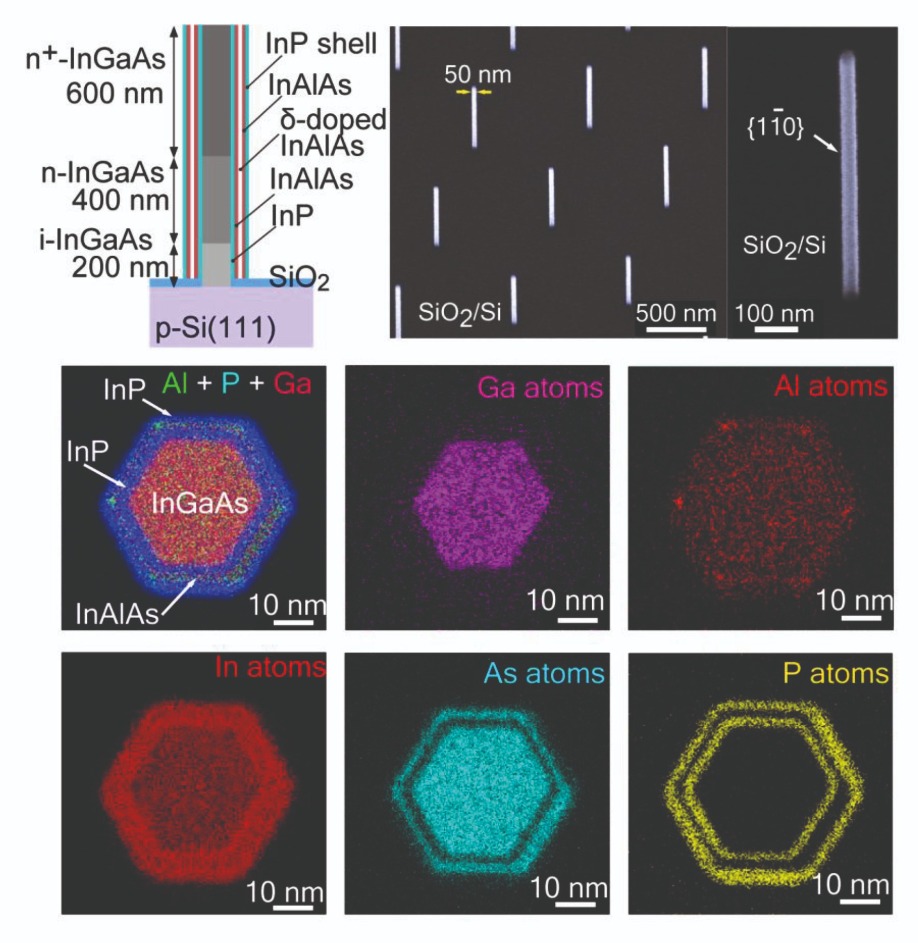
Figure 2. (top left) The structure of vertical III-V nanowires on silicon, formed by direct growth. (middle and bottom) Energy-dispersive X-ray microscopy elemental mapping of nanowires composed of an InGaAs/InP/InAlAs/InP core-multishell structure.
For TFETs, the steepness of the sub-threshold slope strongly depends on the bias condition. Apply a high internal electrical field to the tunnel junction and the addition of a smaller bias realises a steep sub-threshold slope. Thus, by taking care of the series resistance in the TFET, a steep sub-threshold slope may be realised. Alternatively, this can be engineered by combining a moderate tunnel junction with materials with precisely controlled doping and gate stacking technology. The latter approach is the one we have pursued.
One of the challenges with the TFET is ensuring a high enough on-current. As its value is determined by the tunnelling probability, this current depends on junction material characteristics, such as energy gap, effective mass and screening tunnelling length.
We have targeted a high on-current and a low sub-threshold slope when developing our devices. The design that we have trailblazed is a vertical gate-all-around TFET with a vertical InGaAs nanowire/silicon heterojunction and modulation-doped, core-multishell nanowire heterostructure. Selective-area growth is used to form this transistor.
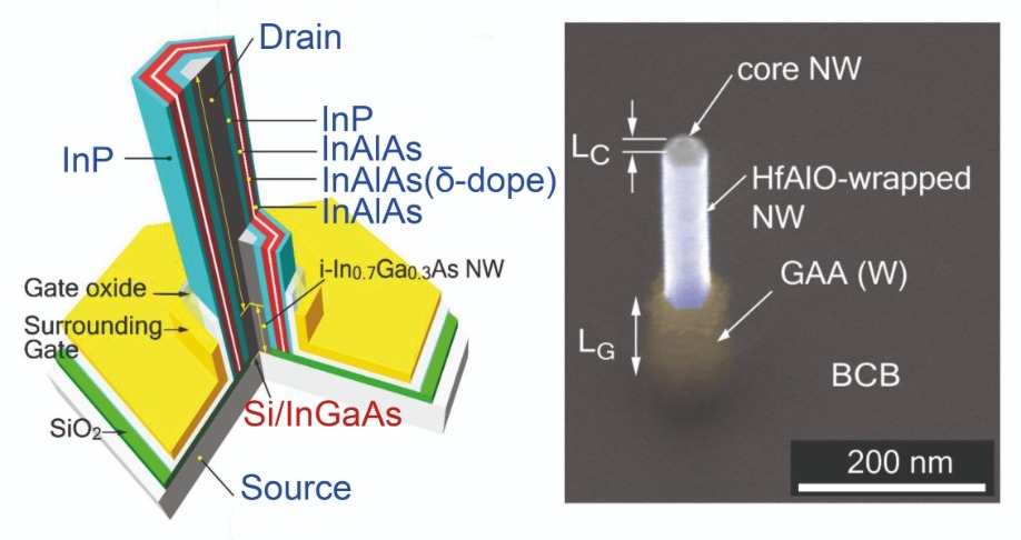
Figure 3. The vertical gate-all-around TFET structure has a core-multishell and a modulation-doping structure. A scanning-electron microscopy image shows the representative device structure formed using a 3D device process.
A representative growth by our team results in vertically integrated nanowires on silicon, based on InGaAs/InP/InAlAs/d-doped InAlAs/InAlAs/InP core-multishell layers (see Figure 2). Within these structures, there is a core In0.8Ga0.2As nanowire-channel with a: 200 nm-long, nearly intrinsic a zinc-pulsed doped layer; a 400 nm-long part with a silicon-doped layer; and a 600 nm-long part, heavily doped with tin. We use this axial junction to adjust the series resistance in the nanowire-channel, and to induce a large internal electric field under low bias. The thicknesses of the InP, InAlAs, d-doped InAlAs, InAlAs, and InP capping layers are about 2.5 nm, 1.0 nm, 1.0 nm, 1.0 nm and 3.0 nm, respectively. Those values indicate that in these heterostructures fine 3D nanostructures can be precisely controlled on the atomic layer scale by selective-area growth. Critical to device performance is the inclusion of the inner InP shell layer, which facilitates the combination of a two-dimensional electron gas and quantum tunnelling.
The structure of our vertical gate-all-around TFET has been fabricated with a 3D device process flow, using a low-k polymer resin, known as BCB (see Figure 3). Wrapping around the sidewalls of the nanowire-channel are a gate oxide, HfAlO composite oxide and tungsten gate metal, all added by atomic layer deposition. We have imaged this structure with scanning electron microscopy, after the reactive-ion process, and can see the core InGaAs nanowire on top of the nanowire channel.
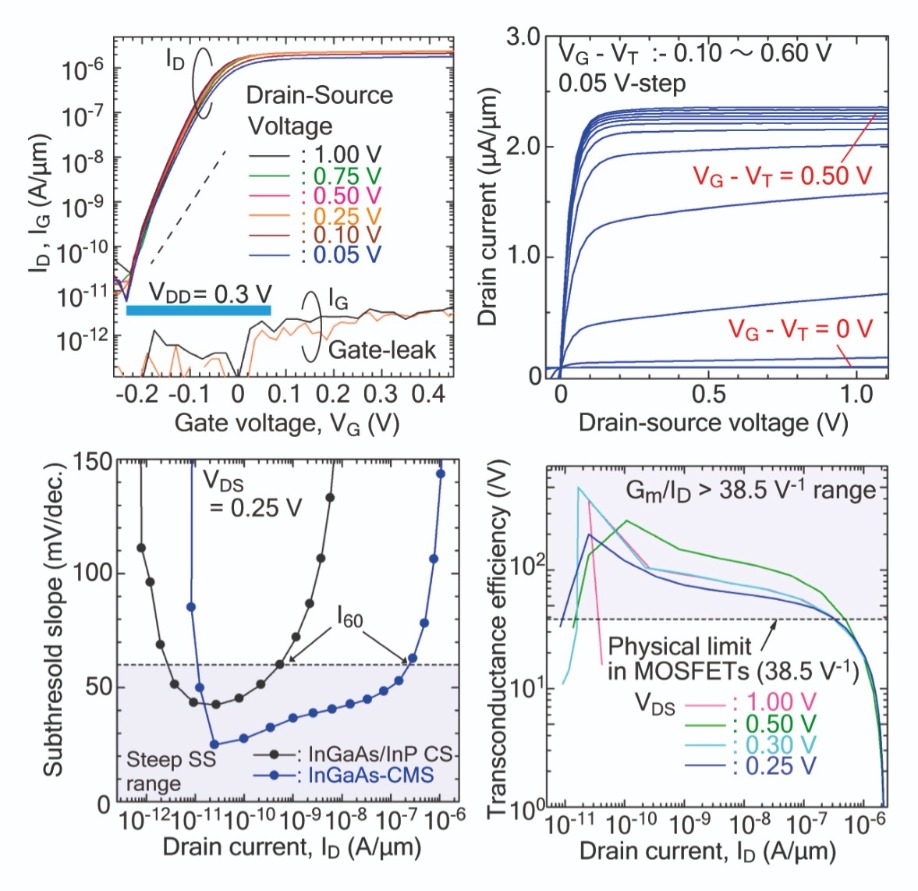
Figure 4 (left). Device performance of the vertical gate-all-around TFET. ID-VG curve shows a steep sub-threshold slope (the minimum sub-threshold slope is 21 mV/dec.) and high ION. The blue bar in this graph is VDD = ~0.30 V. The ID-VD curve exhibits unique output properties. The sub-threshold slope vs ID indicates a steep sub-threshold slope region in the range of about four decades, and a high I60. Transconductance efficiency is much higher than the physical limitation of conventional MOSFETs.
Delivering the promises
To assess the performance of our transistors, we have used a standard setup – a Keysight B1500A or 4156C, with a SMU cable – in a shielded box. Values reported for the current are normalized by the outer perimeter of the core nanowire, which is around 100 nm.
Measurements on our TFETs reveal a steep sub-threshold slope, with a minimum value of just
21 mV/decade (see Figure 4). The gate voltage window for the digital switch is 0.3 V, which is about one third of that of a modern FET. The current region where there is a steep sub-threshold slope extends over around four decades, while the average value for this key characteristic is 40 mV/decade.
The currents produced by our devices are very encouraging. At a 0.5 V supply voltage, the on-current reaches 2.4 mA/μm – that’s a hundred times higher than that for a InGaAs/InP core-shell nanowire/silicon-based vertical gate-all-around TFET. With that design, the core-shell nanowire induces strain inside the core InGaAs nanowire, leading to a slight increase in on-current. Our core-multishell nanowire has the same strain effect, but a far larger current enhancement, thanks to the two-dimensional electron gas in the nanowire channel. The current at a sub-threshold slope of 60 mV/decade is 0.24 mA/μm, which is a thousand times higher than that of the core-shell nanowire/silicon-based vertical gate-all-around TFET.
Plotting the output properties of our devices reveals a unique curve, with a saturation region at a drain-source voltage of around 0.10 V. Insertion of an intrinsically doped InGaAs nanowire segment leads to an absence of the negative-differential resistance, sometimes observed in TFETs, when our device is operated under a negative drain-source voltage (that is a forward bias against p-silicon/i-InGaAs nanowire/n-InGaAs nanowire). A Kane model’s plot shows that the dominant transport mechanism is based on tunnelling.
Another strength of our TFETs is their exceptional transconductance efficiency, which is defined as the transconductance, divided by the drive current. This metric is a measure of the efficiency of the current drive in the ICs. For our devices, its value exceeds the physical limitation of the MOSFET, which is restricted to no more than 38.5 /V. For conventional FETs, this efficiency is virtually zero in the low-current region, while our vertical gate-all-around TFET exceeds this limitation over a wide current range. Transconductance efficiency peaks at around 520 /V at a drain source voltage of 0.25 V.
Note that it is not important that the maximum efficiency is high. Instead, what matters is that this efficiency exceeds the limits of the silicon FET over a wide range of low-current levels. When vertical gate-all-around TFETs are configured with a sufficiently high level of parallelism, there is no longer the need to pursue planar integration of the silicon FETs to try and improve performance as volume decreases (the requirement discussed in Table 1). The vertical gate-all-around TFET is also far better at thermal dissipation.
One other attribute of our TFETs is that, without a change in configuration, they can show p-channel behaviour with a steep sub-threshold swing. We need to look into this device mechanism in more detail, but preliminary investigations show that inverting the ground terminal results in a p-channel switch. The encouraging implication is that by simply aligning the vertical nanowires, a CMOS architecture can be constructed by forming interconnections for the ground terminals.
We have developed the integration of devices based on vertical III-V nanowires on silicon step by step; we began with nanowire HEMTs, nearly a decade ago, and now we have moved on to TFETs with a vertical gate-all-around architecture. We view these technologies as a continuation of Masuoka’s invention that will lead to the next true 3D integration scheme, taking us away from today’s planar integration devices, which have their roots in the 1960s. The vertical III-V architectures that we are pioneering accommodates co-integration and hybrid integration schemes. We are standing on the edge of a technology that will open up a new era, lasting for possibly the next 60 years.
XK. Tomioka et al. Nature 488 189 (2012)
K. Tomioka et al IEEE IEDM Tech. Dig. 429 (2020)
Monolithic integration of III-V devices delivers high-quality detection in the infrared
BY CENK IBRAHIM OZDEMIR AND DRIES VAN THOURHOUT FROM IMEC AND GHENT UNIVERSITY, AND YANNICK DE KONINCK, DIDIT YUDISTIRA, MARINA BARYSHNIKOVA, NADEZDA KUZNETSOVA BERNARDETTE KUNERT, MARIANNA PANTOUVAKI AND JORIS VAN CAMPENHOUT FROM IMEC
IN TODAY’S hyper-connected world silicon photonics has emerged as a key technology for delivering massive data transfer. Several foundries are now offering silicon photonics platforms for the manufacture of electro-optical transceivers with terabit-per-second capacity. These transceivers can serve the growing needs of data communication in hyperscale data centres, as well as in emerging high-performance computing and AI compute clusters.
Silicon photonics is well suited to these tasks, thanks to its high refractive index and transparency at telecom wavelengths, and its capability to carry light efficiently within sub-micron waveguides. These attributes enable photonic ICs (PICs) with a high integration density to offer a scaling path to multi-Tbit/s optical modules for datacom applications, and to provide a pathway for dense optical-phased arrays for future LiDAR systems.
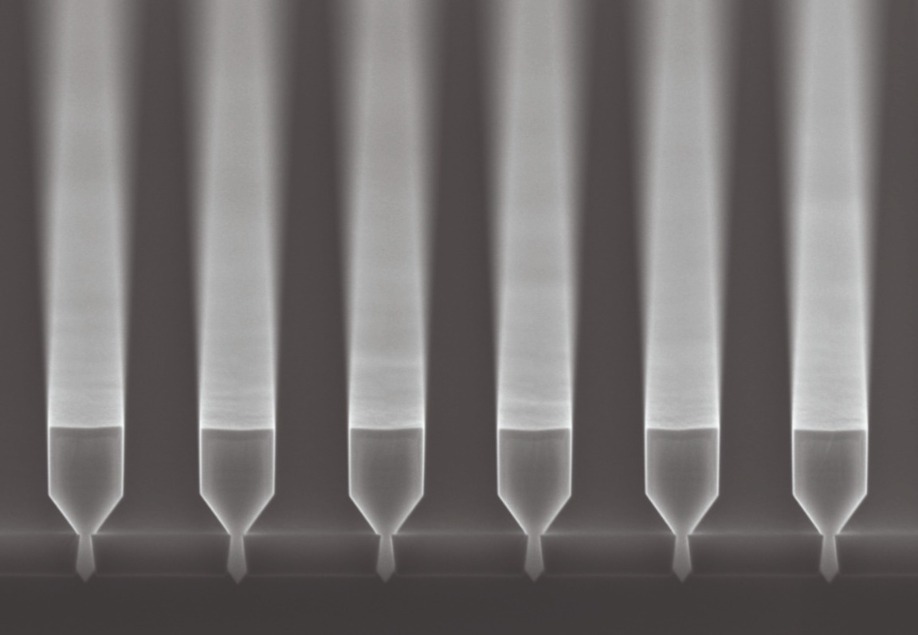
Figure 1. Tilted scanning electron microscopy (SEM) image of III-V nano-ridges grown on silicon.
All that functionality in today’s silicon PICs is partially provided by the monolithic integration of other materials. One of them is germanium, which enables waveguide photodetectors with excellent responsivities out to 1550 nm and acceptable dark currents for high-speed data receivers. However, with germanium, light amplification is still missing from the PIC engineer’s toolbox, as well as photodetection at longer wavelengths – these are valued attributes for a variety of emerging optical sensing applications.
A well-trodden path to overcoming this limitation is to integrate III-Vs onto a silicon photonics platform. Right now, two of the most popular approaches to hybrid III-V integration are flip-chip assembly and die-to-wafer bonding. Both are suitable for serving low to medium wafer volumes. However, in the longer run, arguably monolithic hetero-epitaxial growth of III-Vs directly on silicon offers a more promising pathway to the lowest cost, scalability, and the highest throughput.
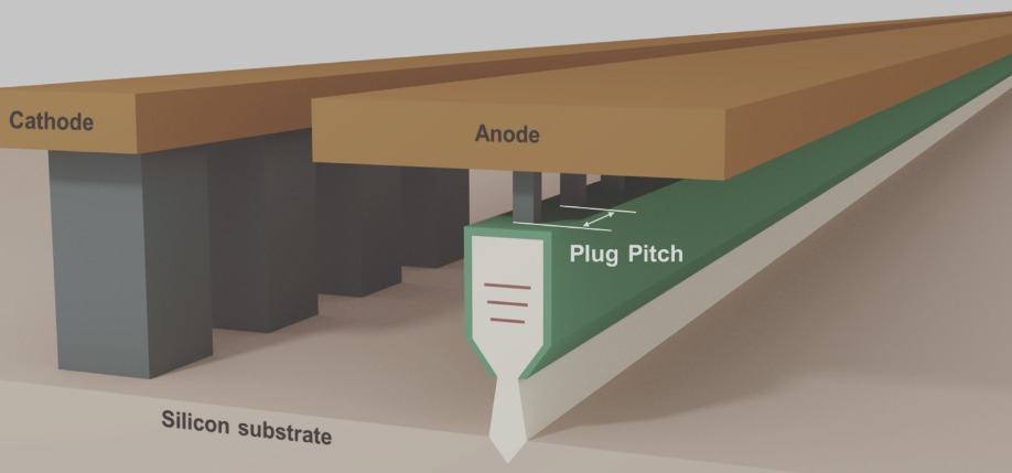
Figure 2. 3D figure of nano-ridge waveguide photodetector devices produced at imec.
Shifting to nano-ridges
At imec, a globally renowned microelectronic research centre based in Belgium, our team is pioneering a unique approach to tackling this issue. With our way forward, which we refer to as nano-ridge engineering, our process for forming devices begins with the selective-area growth of III-Vs in narrow trenches that are patterned on a 300 mm silicon substrate. The high aspect ratio of these narrow trenches traps dislocation defects. After filling the trench, growth of the III-V continues, forming a nano-ridge with an increased volume, an engineered nano-ridge shape, and a very low defect density. By avoiding the need for a thick III-V buffer, this approach results in III-V nano-ridges that are close to the underlying silicon.
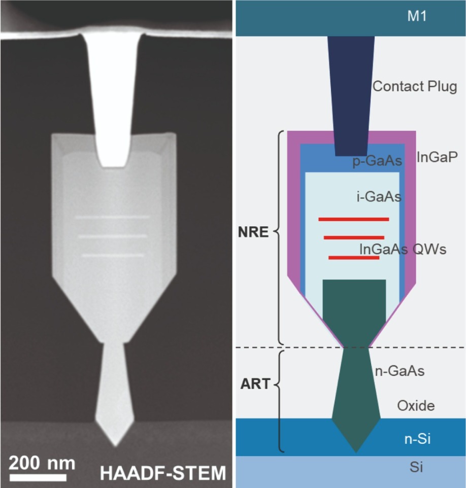
Figure 3. (Right) High-angle annular dark-field scanning transmission electron microscopy (HAADF-STEM) cross-sectional image of GaAs nano-ridge with three InGaAs quantum wells. (Far right) Description of the nano-ridge cross-section. For more details, see C. I. Ozdemir et al. Dec. 2020, pp. 1–4, doi: 10.1109/ECOC48923.2020.9333310
We control the profile of our nano-ridges by adjusting the growth parameters for MOCVD. We have learnt how to engineer a rectangular-shaped nano-ridge with a flat (001) surface, an architecture that provides a great platform for photonics as every ridge provides a waveguide for light and a foundation for making III-V devices.
In addition to controlling the shape of the nano-ridge, our engineering technology enables us to introduce different dopants and III-Vs. We can form diode junctions, introduce quantum wells, alternate between different combinations of III-Vs, and passivate our waveguides.
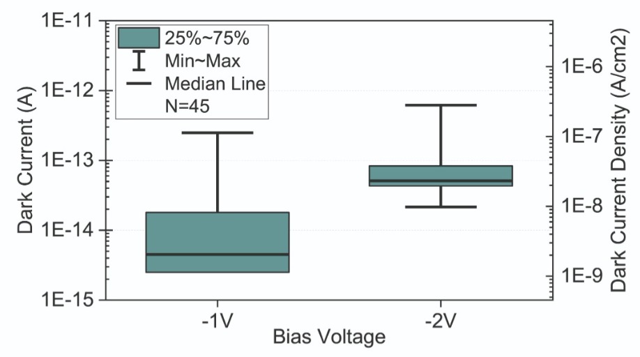
Figure 4. Dark current distribution at different bias voltages. For more details, see C. I. Ozdemir et al. Dec. 2020, pp. 1–4, doi: 10.1109/ECOC48923.2020.9333310
We have used nano-ridge engineering to produce a wide variety of devices. Before our latest work on photodetectors, we developed HBTs. This class of transistor exploits the excellent mobility of the III-Vs for high-frequency RF applications, such as 5G and its potential successors. The attractions of producing HBTs on silicon with nano-ridge engineering include greater flexibility of designs, lower cost and a smaller footprint.
Nano-ridge photodetectors
Recently, we have expanded the range of devices that can be produced on our nano-ridges to include high-quality photodetectors. A key requirement when designing these devices is to make sure that the bandgap of the absorbing material is low enough to capture the light of the desired wavelength. If the device is to have a small footprint, it is also critical that the absorption coefficient of the material is sufficiently high. There are also other potential requirements: if there is a need for a low-noise, highly sensitive detector, the absorbing material must have a low defect density; and if high-speed operation is a must, then the absorbing material needs to have high mobilities for electron and holes, as this enables carriers to be collected quickly. For the last few decades, conventional InGaAs photodetectors fulfilling all of these requirements have been produced in large quantities.
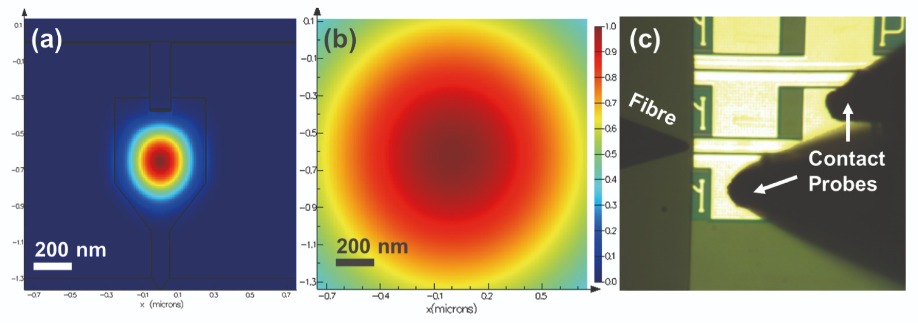
Figure 5. (a-b) Modal cross-sections of a nano-ridge waveguide and a 2.0 µm focused beam, using a linear colour scale. (c) Top view of measurement setup with cleaved facet and lensed fibre. For more details, see C. I. Ozdemir et al. Dec. 2020, pp. 1–4, doi: 10.1109/ECOC48923.2020.9333310
In our latest study, we have evaluated the potential of using a nano-ridge to monolithically integrate high-quality III-V photodetectors on a silicon platform. Using structures for demonstrating optically pumped lasers as the foundation for our recent work, we have developed the expertise to introduce p-i-n doping and create a diode junction, and to add metal contacts to our devices.
We grow our InGaAs/GaAs photodetectors in imec’s 300 mm CMOS line, using MOCVD to add III-Vs to n-doped silicon wafers. By growing these III-Vs in trenches 300 nm deep and 80 nm to 100 nm wide, we have an aspect ratio of more than 3.5, which is high enough to ensure efficient defect trapping. All the threading and misfit dislocation defects initiated at the interface between GaAs and silicon are effectively confined inside the trenches.
During the growth of GaAs, dopants are introduced to define the p-i-n diode, using doping concentrations of about 1.0 x 1019 cm-3 for n-type and p-type GaAs. Absorption of the incident light takes place in three 10 nm-thick In0.20Ga0.80As quantum wells embedded in the i-GaAs layer, shown in Figure 3. To passivate the surface, we cap the rectangularly shaped nano-ridge waveguide with an InGaP layer. After oxide filling, local etching of the InGaP layer and the addition of tungsten contact plugs creates an electrical contact to the top p-GaAs layer. Also, tungsten plugs down to n-doped silicon substrate are formed to contact the n-GaAs end of the device. Standard CMOS copper metallization processing complete device fabrication.
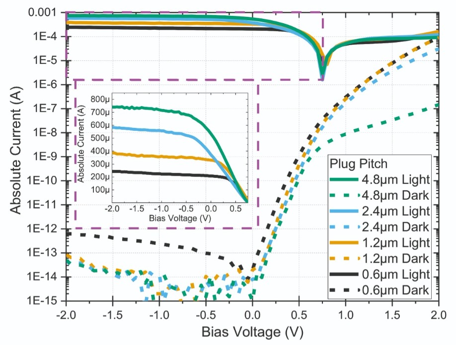
Figure 6. Dark and light measurements of current-voltage (I-V) characteristics of devices with different p-contact plug pitches, (inset) light I-V zoom in at linear scale. For more details, see C. I. Ozdemir et al. Dec. 2020, pp. 1–4, doi: 10.1109/ECOC48923.2020.9333310
In our latest iteration, we cleaved one end of our nano-ridge waveguides to provide optical access from the chip edge to the cleaved optical facet. Cleaving one side of the InGaAs/GaAs nano-ridges yielded 500 μm-long devices.
Before directing light at our photodetectors, we measured their dark current performance under reverse bias. These measurements, carried out under dark conditions – as the name implies – provide an insight into device and material quality. Using typical reverse biases of -1 V and -2 V, we observed very low median dark currents (see Figure 4). For example, at -2 V, we recorded a value of just 0.05 pA, corresponding to a 1.98 x 10⁻⁸ A cm-2 dark current density, calculated by considering the width and the length of our devices. This figure breaks new ground for the dark current of photodetectors monolithically integrated on silicon. Note, however, that the devices we are comparing with operate at higher wavelengths, prone to higher dark currents. That is not to say that our low dark current is not encouraging – it provides a strong indication of good material quality, an essential ingredient for successful monolithic integration.
For our electro-optical measurements, we coupled light into the waveguide through the cleaved facet, using a lensed fibre to provide a beam size of 2.0 μm (see Figure 5). Employing a 1020 nm light source prevented absorption in GaAs, while ensuring absorption in the InGaAs quantum wells.
Due to the small size of our nano-ridge devices, they have a guided mode that is almost five times smaller than the impinging beam. Consequently, coupling losses are inevitable. We evaluated their extent with optical simulation software, which revealed a coupling efficiency of 21 percent. Determining this figure is crucial to estimating of the internal responsivity and quantum efficiency of our devices.
Responsivity is defined as the generated photocurrent, measured in amperes, for each watt of input light power. The maximum theoretical responsivity depends on the wavelength of the incident source, and for 1020 nm it is 0.82 A/W. Our nano-ridge waveguide photodetectors are not far from that upper limit, realising a median internal responsivity of 0.65 A/W at -1 V, recorded for devices with the highest contact plug pitch of 4.8 μm. This equates to an internal quantum efficiency of 79 percent, a high value that shows that even with a comparably small volume, InGaAs quantum wells are successful at absorbing light, while the p-i-n diode is effective at collecting the generated carriers and producing a strong photocurrent.
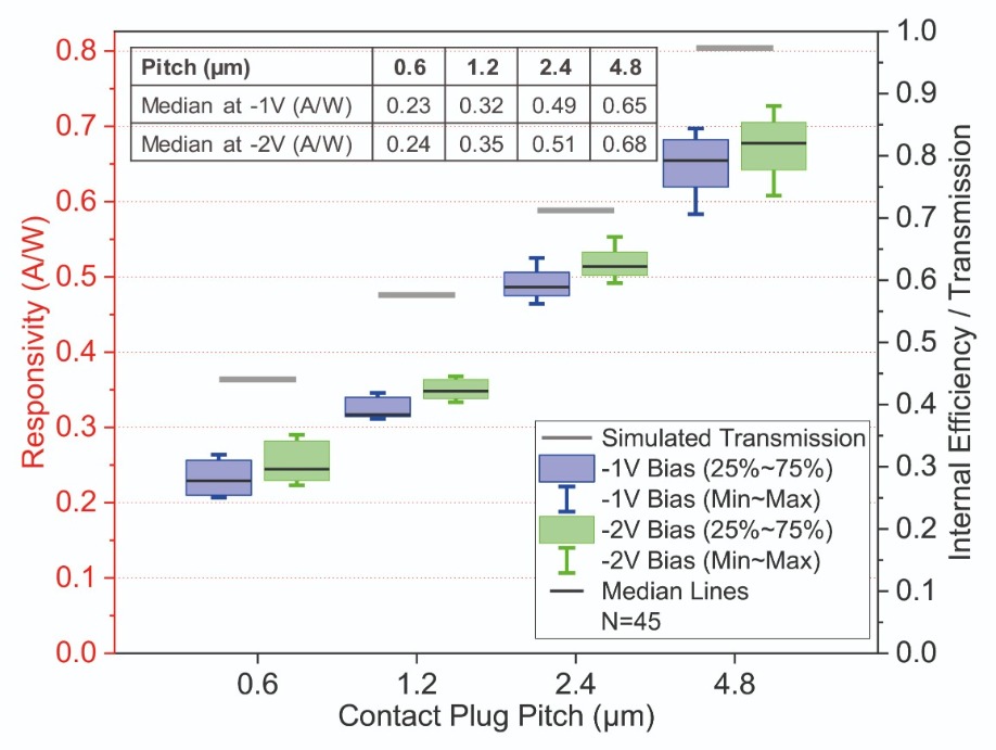
Figure 7. Responsivity distributions for different biases and p-contact plug pitches. Simulated transmission values for different p-contact plug pitches, scaled to right vertical axis. (Inset) Table of median responsivity values. For more details, see C. I. Ozdemir et al. Dec. 2020, pp. 1–4, doi: 10.1109/ECOC48923.2020.9333310
Our successes to date highlight the great potential of our nano-ridge technology for enabling scalable monolithic integration of high-quality III-V optical devices on a silicon platform. With this approach, we have already enjoyed record-breaking performances. The strength of our architecture is that we have a range of building blocks for III-V devices on silicon. Highlighted here are our InGaAs/GaAs waveguides, operating as photodetectors, and InGaAs quantum wells, which are used as active absorbing media but have previously provided optically pumped lasing.
We continue to advance the capability of our technology. Very recently, we have expanded to ternary InGaAs nano-ridges, opening a pathway to integrating devices that function at longer wavelengths. This is yet another step towards the fabrication of optical integrated circuits featuring monolithic integration of III-V devices, formed via nano-ridge engineering on a silicon photonics platform.
The authors are grateful to the fab, metrology and support teams of imec for their dedication in this work. This work was funded by the imec’s industry-affiliation Optical I/O R&D Program
B. Kunert et al. “Gaining an edge with nano-ridges” Compound Semiconductor July 2018, https://www.publishing.ninja/V4/ page/5900/304/6/1
Y. Shi et al. Optica 4 1468 (2017)
Y. Shi et al. Opt. Express 27 37781 (2019)
A. Vais et al. Dec. IEDM 2019, pp. 9.1.1-9.1.4, doi: 10.1109/IEDM19573.2019.8993539
C. I. Ozdemir et al. ECOC Dec. 2020, pp. 1–4, (2020) doi: 10.1109/ECOC48923.2020.9333310
B. Kunert et al. Cryst. Growth Des. 21 1657 (2021)
C. I. Ozdemir et al. J. Lightwave Technol., 2021, (preprint) doi: 10.1109/JLT.2021.3084324
Equipping a normally-off GaN HEMT with a p-FET bridge yields a large, stable threshold voltage
BY MENGYUAN HUA FROM SOUTHERN UNIVERSITY OF SCIENCE AND TECHNOLOGY
GaN IS STARTING to revolutionise power systems by providing higher efficiencies and miniaturization. Its wide bandgap and high saturation velocity enable it to excel in Baliga’s figures-of-merit, and in turn allow power devices made from this material to block high voltages, switch at high frequencies, operate under high temperatures and provide low conduction and switching losses.
Attracted by all these attributes, interest in the deployment of GaN HEMTs is rocketing in many power applications that benefit from higher efficiencies, including electric grids, vehicle electrification, satellites, unmanned autonomous vehicles, photovoltaic systems, and power supplies for data centres.
Today’s GaN HEMTs are not the finished article. One of their biggest roadblocks to fulfilling their potential concerns normally-off operation. To ensure fail-safe operation, end-users want GaN HEMTs to operate in enhancement mode, known for short as E-mode. Chipmakers have responded by launching E-mode GaN HEMTs that tend to realise normally-off operation through the adoption of a p-GaN gate. This design is compromised by a relatively small threshold voltage – it is less than 2 volts (this is for a current on-off ratio of 105). One unfortunate consequence is an increased likelihood of false turn-on during high-speed turn-off transitions, when the gate ring caused by parasitic inductance threatens to exceed the threshold voltage.
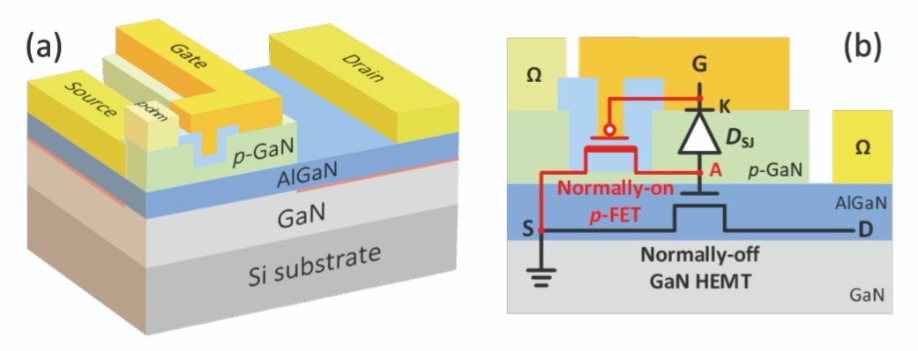
Figure 1. (a) A p-FET-bridge HEMT provides normally-off operation. (b) The equivalent circuit of the p-FET-bridge HEMT. The p-FET and HEMT are drawn on the same cross-section for simplicity, while in the actual device the 2DEG channel under the p-FET is depleted and the p-ohmic connects with the source are outside the p-FET area.
The most common approach to overcoming the challenges associated with low threshold voltage is to use a bipolar gate-drive power supply. Providing a negative gate voltage avoids a false turn-on; but the price that is paid is complexity of gate-drive circuit design. This alternative approach is also hampered by the negative gate voltage, which threatens to accelerate device degradation by attracting the flow of holes to the gate side. The holes are generated by impact ionization in the high electric field region.
In addition to all these issues, there is another associated with a negative gate voltage: an increase in reverse-conduction loss. When GaN HEMTs handle inductive loads, during deadtime these transistors are subjected to a reverse-conduction state that provides a freewheeling current path. This condition is realized by turning on the drain-side channel with a drain-to-gate bias that exceeds the threshold voltage. An unwanted consequence is that the negative gate voltage increases the reverse turn-on voltage of the GaN HEMT and exacerbates loss from reverse-conduction.
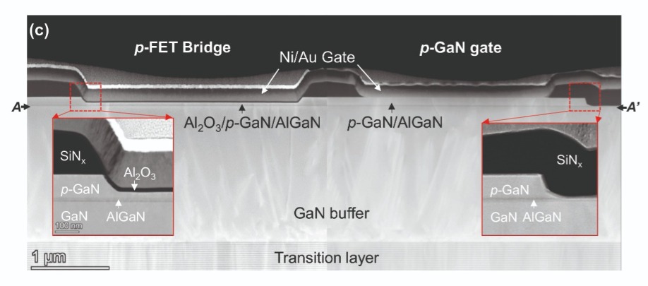
Figure 2. Cross-sectional transmission electron microscopy images of the recessed gate structure in the p-FET bridge and the Schottky-type p-GaN gate stack.
Our breakthrough stems from the introduction of a novel, elegant architecture for E-mode GaN HEMTs (see Figure 1). This design allows us to freely adjust the threshold voltage over a wide range without suffering from drawbacks, such as subthreshold swing degradation and threshold voltage instability. In addition to these very attractive attributes, our transistor inherently enables the decoupling of forward and reverse turn-on voltages.
The pivotal enabler behind our success is the normally-on GaN p-FET that connects the source and the gate. We refer to this architecture as the ‘p-FET bridge’. Outside the p-FET bridge area, our device has the same design as the conventional Schottky-type p-GaN gate HEMT − the gate metal and p-GaN layer form a Schottky junction diode on the top of a normally-off AlGaN/GaN HEMT. In the p-FET-bridge area of our HEMTs, a p-channel is added, connecting the anode of the Schottky junction diode with the source.
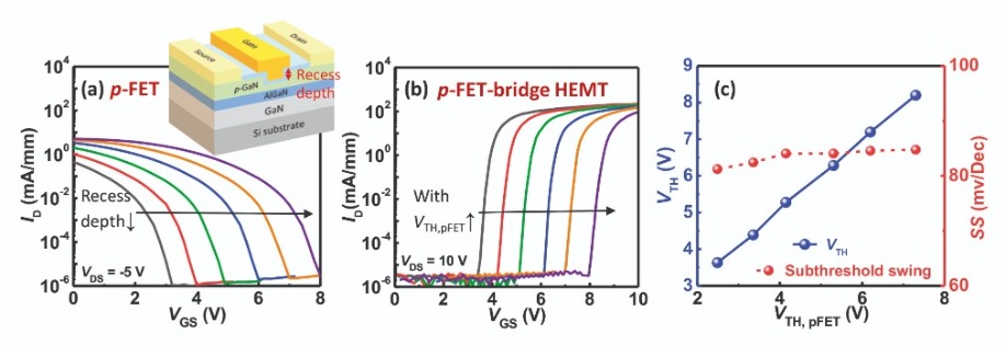
Figure 3. (a) Transfer characteristics of the gate-recessed p-FET with recess depths from 65 nm to 85 nm. The recess depth is estimated with atomic force microscopy after p-FET gate recess etching. (b) Transfer characteristics of p-FET-bridge HEMTs adopting p-FETs with a different threshold voltage (VTH,pFET). (c) Dependence of VTH and subthreshold swing (SS) of the p-FET-bridge HEMTs on VTH,pFET.
An additional advantage of our architecture is its enhanced threshold voltage stability. When the device switches from a large gate or drain voltage back to a smaller one, the emitted holes from the floating p-GaN layer quickly flow back through the p-channel from the source side. This flow of charge helps ensure a stable threshold voltage.
Our technology is relatively easy to pursue, thanks to a readily available p-GaN layer on commercial platforms. With this approach, no complications come from the epi-structure. Another factor in our favour is that although the GaN-based p-FET is not mature enough to consider, that’s not a show-stopper, because we only need a normally-on p-FET. With that particular device it is much easier to achieve a high drain current than it is with an E-mode p-FET.
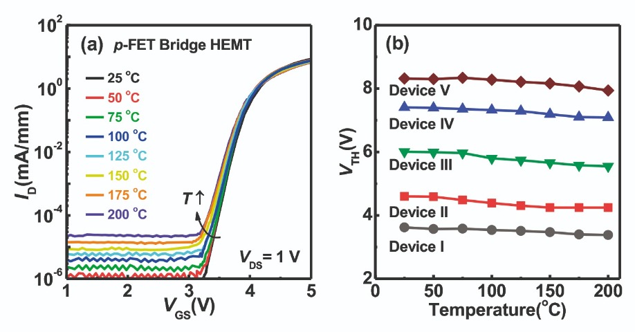
Figure 4. (a) Transfer characteristics of p-FET-bridge HEMTs measured at various temperatures from 25 °C to 200 °C. (b) Temperature-dependence of VTH measured on p-FET-bridge HEMTs with different VTH.
Concept demonstration
To produce our devices, we begin with 6-inch GaN-on-silicon wafers designed for E-mode p-GaN gate HEMTs. These epiwafers have a 4.2 μm-thick high-resistivity GaN buffer, a 420 nm GaN channel, a 15 nm-thick Al0.15Ga0.85N barrier, and a 100 nm p-GaN cap that is doped with magnesium to a level of 4 x 1019 cm-3. From this heterostructure we form HEMTs with a 3 μm gate length and a 15 μm gate-to-drain spacing. The later ensures a blocking voltage of more than 600 V.
Device fabrication begins by removing the p-GaN outside the gate region, accomplished with an inductively coupled plasma etcher that employs a combination of chlorine and boron trichloride gases. During this etch, we protect the p-GaN with an e-beam evaporated chromium layer. This is a better choice than a dielectric film − such as a SiNx, SiO2 or Al2O3 layer that can be deposited by PECVD or ALD − because chromium prevents plasma damage on the p-GaN surface and hydrogen incorporation in p-GaN. Ultimately, this ensures good p-type ohmic contacts.
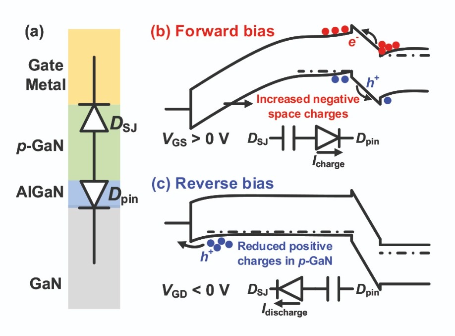
Figure 5. (a) Equivalent circuit of the Schottky-type p-GaN gate stack. The band diagram along the gate stack under (b) forward bias and (c) reverse bias.
After device fabrication, we use an implanter to provide planar isolation. Our final steps are to remove the Al2O3 layer outside the p-FET gate region and add gate electrodes and probing pads, comprised of 20 nm-thick nickel and 100 nm-thick gold (see Figure 2 for a scanning transmission electron microscope cross-sectional image of this fabricated device). To benchmark our devices, we have also fabricated individual p-FETs and conventional p-GaN gate HEMTs from the same epi-wafer.
Freely adjustable threshold voltages…
By adjusting the turn-on voltage of our p-FET, we freely modulate the threshold voltage of our p-FET-bridge HEMTs over a wide range (see Figure 3).
Electrical measurements on a range of our devices reveal the impact of the depth of recess etch on normally-on operation (see Figure 3 (a)). Varying this depth from 65 nm to 85 nm shifts the threshold voltage from 2.4 V to 7.3 V, with a shallower recess depth providing a more positive threshold voltage.
The forward saturation current for our p-FETs is 5.4 mA/mm, but far higher values may be possible by employing more elaborate techniques. In our bridged devices, the p-FETs are always operated in the reverse-conduction region, with a gate bias higher than 0 V. One merit of this is that it avoids a large shift in the threshold voltage induced by a negative gate bias in the on-state. Consequently, the p-FET has a more stable threshold voltage in the –-FET-bridge devices.
By adjusting the turn-on voltage, we can alter the threshold voltage from 3.6 V to 8.2 V in a linear manner. Encouragingly, the subthreshold swing shows negligible degradation when making large adjustments to the threshold voltage. Under the same gate over-drive bias – that is, the difference between the gate voltage and the threshold voltage – the on-resistance is similar for p-GaN gate HEMTs with and without a p-FET bridge. Although the 2DEG channel is depleted under the p-FET bridge, it may be possible to maintain a low total on-resistance thanks to the common access region outside the bridge area.
We have also evaluated the thermal stability of the threshold voltage. To do this, we measured the transfer characteristics of several p-FET-bridge HEMTs, each with a different value for the threshold voltage. All of the tested HEMTs have a small variation in threshold voltage up to 200 °C – it is less than 0.4 V (see Figure 4).
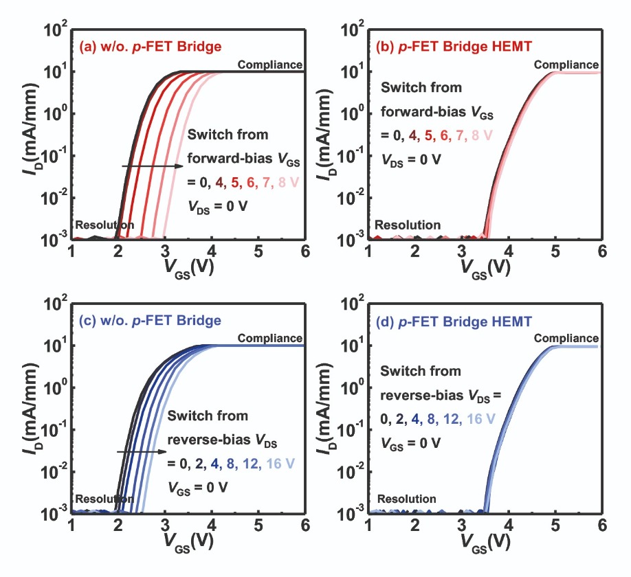
Figure 6. Transfer characteristics of (a) (c) the conventional Schottky-type p-GaN gate HEMTs, and (b) (d) p-FET-bridge HEMTs measured immediately after a 1 second hold under forward- (red curves) and reverse-bias (blue curves).
Under reverse conduction, the p-GaN gate is always shorted to the source via the p-FET channel, ensuring that the HEMT behaves like a gate-injection transistor in this specific operation condition. Due to this, the reverse turn-on voltage is determined by the threshold voltage of the normally-off gate-injection transistor. Operation in this manner ensures that the reverse conduction capability of the 2DEG channel is fully utilized with no area sacrificed. By utilizing this property, it is possible to realise p-GaN gate HEMTs with lower on-resistance, higher threshold voltages, and lower reverse turn-on voltages by introducing the p-FET bridge.
… and enhanced stability
With conventional p-GaN gate HEMTs, there is the threat of a shift in threshold voltage during switching. In these devices the Schottky-type p-GaN gate can be regarded as one Schottky junction diode and one p-i-n diode, connected in series. Under forward bias with high gate bias, the p-i-n diode is forward biased, driving hole injection from the p-GaN to the channel and charging up the Schottky junction capacitor (see Figure 5 (a)). This leads to an increase in the negative space charge in the p-GaN layer.
When these conventional devices operate under reverse bias with a high drain bias, holes are emitted through the Schottky diode, discharging the p-i-n capacitor (see Figure 5 (b)). Thus, there are fewer holes in the p-GaN. Switching the gate and drain voltages back to a lower level results in hole deficiency, due to the Schottky barrier blocking speedy replenishment of holes into the p-GaN layer. Eventually, positive threshold voltage shifts are observed (see Figure 6).
A significant advantage of our design is that the floating p-GaN layer is shorted with the source. This ensures a stable threshold voltage, with holes immediately flowing back to p-GaN after switching from a high-stress voltage to a lower level.
In short, our HEMT design excels in delivering a stable threshold voltage that is adjustable over a wide range. This is an important breakthrough, taking this device a step further to providing widespread high-efficiency energy conversion.
M. Hua et al. ‘E-mode p-FET-bridge HEMT for Higher VTH and Enhanced Stability’, in 2020 IEEE International Electron Devices Meeting (IEDM), December 12-18, 2020
J. Chen et al. “Decoupling of Forward and Reverse Turn-on Threshold Voltages in Schottky-Type p-GaN Gate HEMTs,” in IEEE Electron Device Letters, doi: 10.1109/LED.2021.3077081

Photoluminescence spectra obtained at cryogenic temperatures unveil p-doping levels in GaN
OPTIMISATION of the GaN MOSFET has been held back by difficulties in measuring the low levels of p-type doping employed in this power transistor. But this problem persists no longer, thanks to the work of a Japanese team from Oita University and Mirise Technologies. By using low-temperature photoluminescence measurements to unveil magnesium-based p-type doping levels over a very wide range, these researchers have trailblazed an alternative approach that is simple, non-destructive and non-contact.
While the cost of a low-temperature photoluminescence set-up is not insubstantial – the bill for a cryostat, spectrometer, detector and laser totals about $200,000 – it comes in at less than the alternatives, according to team spokesman Masato Omori from Oita University. He points out that conventional electrical measurement equipment, such as that based on the Hall effect, has a price tag of around $300,000, and says that it can cost more than $1 million to purchase device process equipment, used to form electrodes, etch material and dice wafers.
“In addition, wafers can be used directly in devices after the photoluminescence measurement,” argues Omori, “while wafers for electrical measurements are disposable and therefore wasteful.”
Another important consideration is that the process for forming an ohmic electrode with a low-concentration of p-type GaN – that is, less than 1 x 1018 cm-3 – is yet to be established. “The development of such technology requires a great deal of cost and time,” remarks Omori.
The technique that he and his co-workers have pioneered follows in the footsteps of Michio Tajima, who worked at the Japan Aerospace Exploration Agency in 1970s. During his time there, Tajima developed a method for quantifying the dopant concentration in silicon, based on considering the ratio of the intensity of the impurity-bound exciton line to the free exciton line. It is this ratio that Omori and co-workers are using to determine the magnesium acceptor concentration in GaN samples.
To establish this technique, the team produced five samples, containing 2 μm-thick GaN layers with a range of magnesium doping levels from 5 x 1016 cm-3 to 1 x 1018 cm-3. After capping these epilayers with 100 nm of SiO2, they annealed the samples for 5 minutes under nitrogen gas at 1050 °C to activate the dopants. Prior to photoluminescence measurements, the samples were etched to remove the SiO2 cap and the magnesium segregated layer near the surface.
Photoluminescence measurements at 40K produced several peaks, including those associated with the neutral magnesium acceptor-bound exciton and the free exciton (see Figure 1). The ratio of the intensity of these two peaks has a power-law dependence with the magnesium concentration, measured by secondary-ion mass spectrometry (see Figure 2).
The power law established by the team could also be used to determine p-doping levels in LEDs, laser diodes and HEMTs. “However, these devices have high impurity concentrations that are relatively easy to measure electrically, so my technique may not be as beneficial,” says Omori.
According to him, one of the team’s next goals is to create calibration curves for other impurities, such as silicon donors. “Also, since the ion implantation technique has not yet been established for GaN, I am considering applying my technique to its development.”
Reference
M. Omori et al. Appl. Phys. Express 14 051002 (2021)
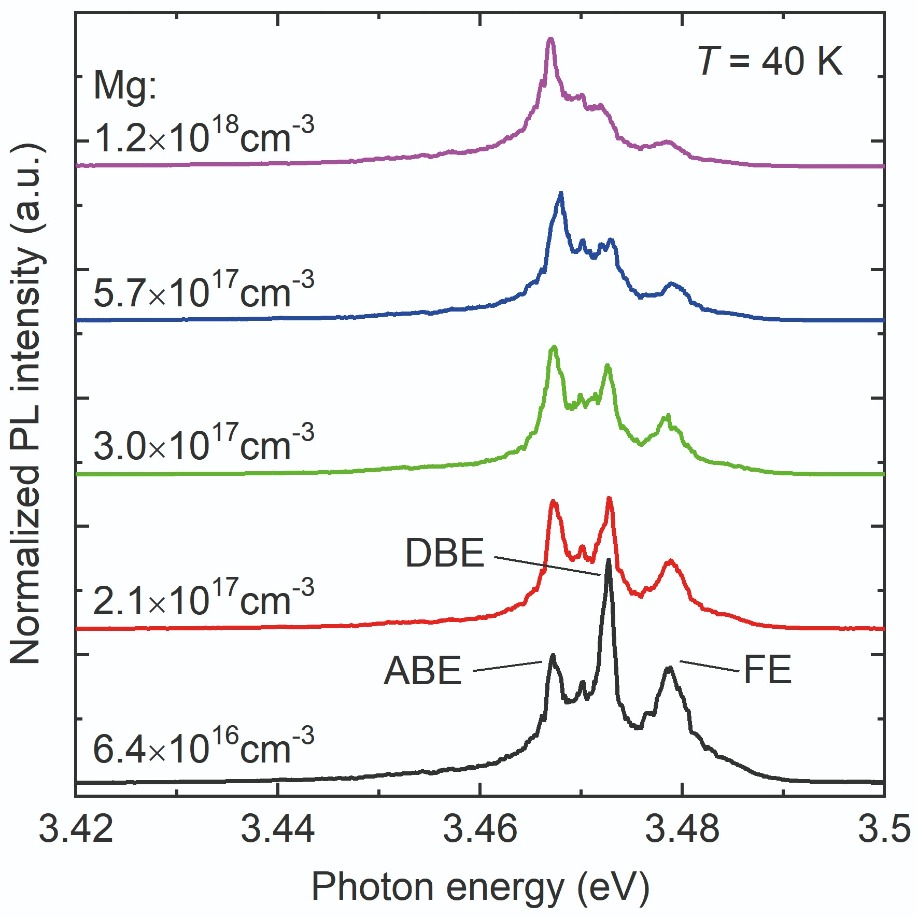
Figure 1. Photoluminescence measurements at 40K produced peaks associated with the neutral magnesium acceptor bound exciton (ABE), the free exciton (FE), and the neutral donor bound exciton (DBE).
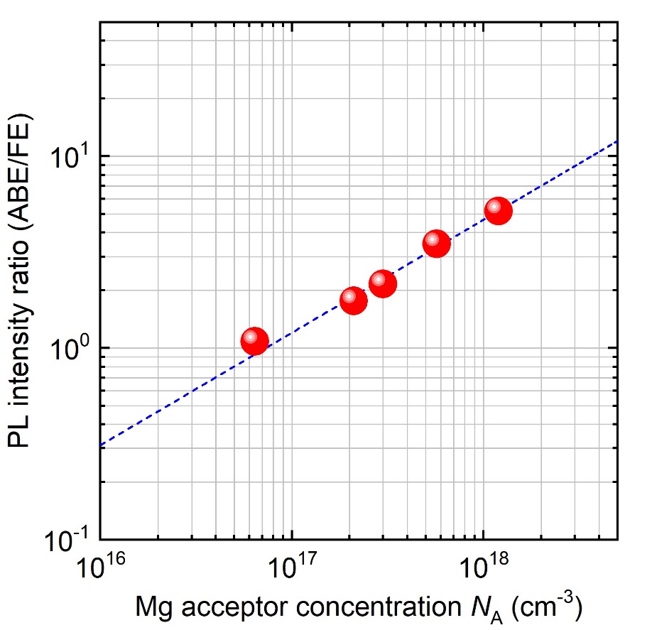
Figure 2. Thanks to a power law, magnesium doping levels can be extracted for photoluminescence measurements, by determining the ratio of the intensity of the peak for the neutral magnesium acceptor bound exciton to that of the free exciton.

Ammonia-free growth of crystalline AlN results from high-temperature microwave plasma CVD
ENGINEERS at Beijing University of Technology and Suzhou Institute of Nano-Tech and Nano-Bionics claim to have made substantial progress in growing AlN epilayers with a novel deposition technology.
According to the team, traditional approaches for depositing epilayers, namely MOCVD and MBE, struggle to reach the temperatures of 1400 °C of more that are ideal for the growth of crystalline AlN. Such high temperatures are preferred because they ensure sufficient mobility of aluminium adatoms.
By turning to microwave plasma CVD, the team from China has produced high-quality AlN films at elevated temperatures.
Microwave plasma CVD, which is primarily used for growing diamond, involves heating a substrate by a high-temperature plasma containing growth sources, with heat transferred by conduction and radiation.
One merit of microwave plasma CVD is that, unlike MOCVD and mainstream MBE, it does not use ammonia for the nitrogen source. Ammonia has many drawbacks: it is toxic and corrosive; it is harmful to the environment and the equipment chamber; and it undergoes pre-reactions with precursors, hampering material quality.
The Chinese collaboration is following in the footsteps of research in the 1990s on the growth of AlN by microwave plasma CVD. However, those efforts were restricted to temperatures of around 500 °C, a limitation that impacted material quality.
To grow AlN epilayers, the team began by loading 6H-SiC substrates into their home-built microwave plasma CVD system. A 5.6 kW source, emitting at 2.45 GHz, generated microwaves that travelled through the waveguide, entered the reaction chamber and concentrated in the upper regions of the molybdenum tray. These microwaves heated the substrate and activated the plasma of carrier gas and precursors.
Trimethylaluminium and nitrogen provided the group III and V sources, with the latter also acting as a carrier gas. Using flow rates for trimethylaluminium, nitrogen and hydrogen of 38.6 mmol min-1, 330 sccm and 165 sccm, respectively, the engineers deposited AlN films at a range of temperatures from 1200 °C to 1500 °C. Even higher growth temperatures could be realised by turning to a higher chamber pressure and a more powerful source of microwaves.
An hour’s growth at temperatures of 1300 °C, 1350 °C, 1400 °C and 1450 °C produced AlN films with thicknesses of 540 nm, 520 nm, 510 nm and 490 nm, respectively. No growth occurred at 1200 °C, because at this temperature the activity of nitrogen gas is insufficient to decompose and react with the group III source; and at 1500 °C, excessive etching by hydrogen gas prevented deposition of an AlN film.
According to high-resolution X-ray diffraction spectra, higher growth temperatures led to better material quality. For an AlN epilayer grown at 1450 °C, values for the full-width at half-maximum in the (0002) and (1012) directions were 142 arcsec and 350 arcsec, respectively.
The team attributed the superior crystal quality at higher growth temperatures to increased adatom mobility and greater etching by the hydrogen plasma. The etching is more prevalent in poorer quality domains, which are more amorphous and have a greater proportion of polycrystalline content.
Insights provided by X-ray photoelectron spectroscopy enabled an assessment of the stoichiometry of the epilayers. The ratio of aluminium-to-nitrogen is 1:0.95 in the AlN film grown at 1300 °C, and equal in that formed at 1450 °C. This finding supports the conclusion from X-ray diffraction measurements that higher growth temperatures ensure better material quality.
Higher growth temperatures also produce smoother films, according to atomic force microscopy. Epilayers grown at 1300 °C have a root-mean-square surface roughness of 3.6 nm, compared with 0.6 nm and 0.8 nm for AlN layers grown at 1400 °C and 1450 °C, respectively.
Reference
Y. Zhang et al. Appl. Phys. Express 14 055503 (2021)
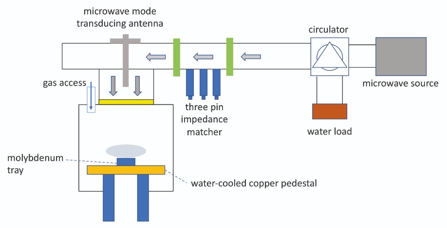
Using nitrogen and trimethylaluminum sources, microwave plasma CVD produces high-quality AlN films.

Growth of diamond layers, realized through high-density seeding of diamond nanoparticles, combats the low thermal conductivity of gallium oxide
FOR Ga2O3, substantial strengths go hand-in-hand with significant flaws. Thanks to an ultra-wide bandgap, this oxide can withstand very high electric fields, giving it the potential to outperform devices made from SiC and GaN. And unlike those two rivals, Ga2O3 enjoys melt growth of bulk material. However, it is plagued with a lack of p-doping, and a pitiful thermal conductivity of typically just 11-27 W m-1 K-1.
Helping to address the latter issue is a US collaboration that has recently broken new ground by depositing a high thermal conductivity layer, in this case diamond, directly onto a Ga2O3 layer.
Team spokesman, Srabanti Chowdhury from Stanford University, emphasised the importance of this breakthrough by telling Compound Semiconductor that improving heat extraction is crucial for the progress of Ga2O3 power and RF devices. “However, this thermal management must be cost-effective for both applications, and particularly so for power electronics.”
Cost-constraints hamper the use of large-area single-crystal diamond wafers, which are pricey and limited in size and availability. It is also worth noting that this form of diamond does not give the best results. The thermal boundary resistance for structures constructed by placing small pieces of single-crystal diamond, typically just 3 mm by 3 mm in size, onto Ga2O3, is around 60 m2 K GW-1. A similar figure is found when transferring exfoliated Ga2O3 onto single-crystal diamond, but for the structures produced by the US team, featuring polycrystalline diamond, the thermal boundary resistance is only about 30 m2 K GW-1.
“Our measured diamond-gallium oxide thermal boundary resistance is comparable to those reported for CVD-grown diamond on GaN with about the same silicon nitride dielectric interlayer, which is a very promising result,” enthuses Chowdhury.
The team from Stanford University, The Pennsylvania State University, Georgia Institute of Technology and the University of California, Davies, had to develop a novel process for growing diamond layers. That’s because the direct growth of a diamond layer, by microwave plasma CVD, leads to decomposition of the substrate.
To overcome this issue, the researchers investigated three different approaches to realizing high-density seeding: ultrasonication in a nanoparticle solution, drop-seeding, and polymer-assisted seeding.
Ultrasonication seeding failed to realise a continuous layer of diamond. Diamond nanoparticles tended to agglomerate, resulting in a β-Ga2O3 surface unprotected from the plasma. Substrate decomposition followed.
Drop-seeding enabled the deposition of a diamond layer, but it suffered from non-uniformity, due to a very thick seeding layer. And due to differences in thermal expansion coefficient, the diamond delaminated once its thickness exceeded about 200 nm.
Polymer-assisted seeding produced the best results. The reserachers developed a self-assembly approach, using the polymer to prepare a negative electrostatic surface, before adding nanoparticles with a positive zeta potential. This populated the surface with nanoparticles at a density exceeding 1012 cm-2. However, due to the high decomposition rate of β-Ga2O3 in a hydrogen plasma, hydrogen ions threatened to pass through the nanoparticles and inflict damage on the surface of the oxide. To prevent this, the team inserted a thin layer of SiO2 between the β-Ga2O3 and the diamond nanoparticles. This led to the growth of diamond layers.
Measurements on a sample with a 19 nm-thick layer of SiO2 and a 267 nm-thick layer of diamond revealed a thermal conductivity of 110 W m-1 K-1.
Efforts will now be directed at lowering the thermal boundary resistance and increase the thickness of the polycrystalline diamond, without degrading the properties of Ga2O3.
Reference
M. Malakoutian et al. Appl. Phys. Express 14 055502 (2021)
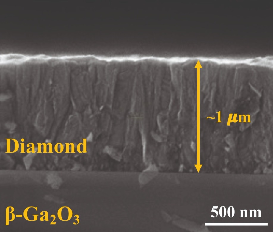
Growth of a diamond layer on Ga2O3 realised by adding a thin layer of SiO2 and polymer-assisted seeding of diamond nanoparticles.

According to Precedence Research in a report from January 8, 2021, the global electric vehicle market is expected to grow by more than 40% by 2027. What it says, among other things, is that the supply chain for chips and modules powering these vehicles needs to evolve immediately. One of the obvious shifts will be moving away from traditional devices made from silicon and toward devices made from compound semiconductor materials such as silicon carbide (SiC). At higher voltages needed for EV’s, the performance properties of SiC far outpace those of silicon, but the supply chain for SiC is not nearly as mature. The global EV market needs SiC to catch up…and quickly.
Integrated Device Manufacturers (IDMs), already well-versed in silicon, needed a pathway to produce SiC devices and modules for rapidly accelerating EV demand. But SiC is more complex because it comes from a crystal that is extremely difficult to grow, and that presented a bottleneck. It is against this backdrop that GTAT (www.gtat.com) began forging a business model in 2017 to become a ‘pure-play’ producer of wafering-ready SiC. The Company’s focus on growing SiC bulk crystal and staying away from wafering and device-making is an important distinction. “We have a core competency, and that’s crystal growth,” says GTAT President and CEO Greg Knight. “There are tremendously talented companies around the world that know how to make wafers and devices, but what they don’t necessarily have is a way to grow the SiC crystal. They need the material, and lots of it.”
GTAT’s heritage as a producer of crystal growth equipment means that it can ‘scale up’ capacity very rapidly. The knowhow needed to design and build crystal-growth furnaces is the essence of GTAT’s DNA. “We are able to bring SiC capacity to market faster than anyone,” said Knight. Indeed, the Company has hit milestones extraordinarily rapidly. “We made our CrystX® silicon carbide n-type material available to customers in 2018, less than a year after opening our facility,” said Knight. A year after that GTAT achieved ISO 9001:2015 certification and signed the first of several long-term supply agreements with key customers for 150mm diameter boules.
Fundamentally, SiC is not a defect-free material and is challenging to make at the high quality levels customers demand. That is why most of the companies invested in making SiC wafers and devices do not have the experience to also make the crystal material itself. The equipment used to make silicon cannot be used for SiC, and the capex (and time) required to develop in-house SiC growth is significant. “We understood this early-on,” said Knight. “We knew that SiC was going to become the base material for semiconductors used in growing applications such as EV.”

Specifically, Etch Pit Density (EPD) and Basal Plane Dislocations (BPD) are critical quality metrics for SiC. GTAT has made significant progress driving down BPD’s to less than 1,000 per cm2 and is set to reduce this by another 50% in the near term. Much of GTAT’s focus has been on reducing defects through continuous improvement. “This is what our customers demand, and we deliver,” said Knight.
“We have a longstanding heritage in building the equipment we now use ourselves, and we couple that with a high level of process excellence.” GTAT’s inherently stable production process enables all its high-quality material to be made to this standard, which is available under a single product grade.
While continuous improvement is a function of GTAT’s increased cycles of learning and optimization, R&D efforts allow the company to push forward on 200mm diameter SiC as well as semi-insulating (SI) SiC for RF applications. Both product launches are expected in late 2021 or early 2022. To support existing 150mm demand while forging ahead with 200mm and SI, GTAT is currently growing production capacity by 60% on top of what exists today. With multiple supply agreements in place, the ability to ramp up quickly puts GTAT in a perfect position. “Rapidly growing markets like EV require a very nimble supply chain, and we’re able to respond,” said Knight. This round of expansion will be completed by early Q3 2021, with more expected as partners continue to scale their demand.

Introduction of 200mm diameter. SiC will occur later in 2021
The 78% increase in wafer surface area means a corresponding increase in the number of devices, which helps lower cost. “Higher quality and bigger-diameter boules are parallel efforts for us,” said Knight. “We are moving very rapidly in response to a very dynamic and fast-growing set of markets.”

GTAT will be expanding its production capacity by 60 percent in 2021.
From EV’s to 5G, the global push to ‘electrify everything’ is resulting in a need for circuits and devices that have performance capabilities that extend well beyond those afforded by silicon. While SiC is seen as a front-running material to meet this challenge, demand for it far exceeds supply. This is because most producers of silicon cannot add SiC to their portfolios without investing in an entirely new process and undergoing a very steep learning curve. This is where a ‘pure-play’ SiC producer such as GTAT becomes valuable on a global scale. As GTAT boosts the ‘non-captive’ global supply of high-yield, high-quality SiC, devices made from SiC become more affordable. This means higher performance and lower system-level costs. In practical terms, EVs can enjoy better range thanks to increased use of more electrically efficient SiC. Also, the affordability index for EVs will increase over time as SiC becomes more prevalent.

GT Advanced Technologies is a manufacturer of high-performance crystal materials including silicon carbide (SiC) and sapphire. GTAT’s corporate headquarters in Hudson, New Hampshire also serves as the Company’s primary manufacturing facility for its CrystX silicon carbide. This material is fundamental to the production of semiconductors used in electric vehicles and other power electronics applications.
Directly contact:
Christopher Van Veen
chris.vanveen@gtat.com for more information, or visit us at:https://gtat.com/products/silicon-carbide

