


SOME SOLUTIONS only get you so far. Initially, they show promise, providing ground-breaking results. But then they stutter, hit a wall, and never make enough progress to enable a commercial product.
This is what happened at Nichia a decade or so ago, when developing a GaN VCSEL. In 2008 it broke new ground when producing the first ever GaN VCSEL operating at room temperature, and kicked on for the next few years, improving output power. But there were concerns over reliability and reproducibility, with progress appearing to grind to a halt. Nichia did not announce any results for nearly a decade, leaving many to wonder if it had abandoned work on this device for good.
Now we know that’s clearly not the case. At this year’s Photonics West, the company claimed to have produced the world’s most efficient blue and green VCSELs. Now, rather than using a pair of dielectric mirrors for its device, it is combining one of them with another based on the nitrides. This is an approach pioneered by Nicolas Grandjean and co-workers at EPFL, Switzerland, and refined by Tetsuya Takeuchi’s team at Meijo University that has recently worked with engineers at Stanley Electric.
Nichia’s recent success comes at a time of great progress for GaN-based VCSELs. Developers of these devices are making great strides in decreasing the emission wavelength. In this issue you can read about the efforts of a European collaboration, led by researchers at Chalmers University, to realise emission down to a very impressive 310 nm.
The last few months have also witnessed the launch of an alternative to the VCSEL – the photonic crystal surface-emitting laser (PCSEL). Pioneered by Vector Photonics, a Scottish start-up that has drawn on research from the University of Glasgow, the PCSEL is said to combine the best attributes of the edge-emitting laser and the VCSEL. Majoring on its combination of high-speed, low-cost and power, the PCSEL also offers a step change in data rates, and the capability to span a vast spectral range.
Vector Photonics is initially targeting the datacoms markets, arguing that this is the only source capable of meeting the requirements for next-generation, high-data-rate lasers. But plans are also in place to see this device deployed for plastic and metal printing, as well as mobile consumer and sensing applications. Although it is now almost 60 years since the invention of the laser diode, as you’ll continue to see from this magazine’s coverage, device development continues at great pace, leading to improvements in numerous characteristics.

As microLED patent numbers sky-rocket, Eric Virey, senior industry analyst at Yole Développement, discusses what could happen next in an interview with Rebecca Pool
RP: YOLE DÉVELOPPEMENT research indicates that nearly 9000 patents relating to micro-LEDs have been filed by some 480 organisations – where did this all start?
YD: The concept of microLEDs was developed in the early 2000s, with a handful of companies and research organisations showing an interest. But it was LuxVue’s acquisition by Apple in 2014 that really put the microLED on the map. From that moment, the technology started getting the attention of established display makers as well as other OEMs, with patents then starting to get filed. You typically have a six to 18 month delay between patent filing and publication, and so we have seen this huge acceleration in patent activity from around 2017.
RP: Will we continue to see this acceleration in the number of microLED patent applications?
YD: It remains to be seen if the Covid-19 pandemic has temporarily slowed applications but overall I’m expecting the trend to continue. We’ll have to wait and see if exponential growth continues, but it’s definitely going to keep increasing as there is such strong momentum right now. This might be a little bit of a bubble or self-fulfilling prophecy as so many companies see competitors working on microLEDs, and think ‘we need to invest in microLED as well’.
RP: What’s the situation in China on microLED patents?
YD: Geographically, China’s now the largest single driver of microLED intellectual property. Just last year almost 45 percent of new patents originated from China-based companies – this mirrors the overall trend in intellectual property in China. The nation is transitioning from a manufacturing- to innovation-driven economy. And of course, patents are a key tool for that.
RP: How has content of microLED patents changed over time?
YD: Besides LuxVue, which had advanced patents very early on, many followers were filing very generic patents back in 2017. These basically said ‘take your LED, make it very small and assemble it in a matrix’ – you could tell these companies were just planting a seed in the ground and not really trying to solve actual challenges. But this has now changed dramatically and many companies, including big names such as Samsung and LG, are really working on making this happen. Patents are now going into great detail on design and manufacturing – and this is a trend we’re seeing in China. We have seen many ‘junk’ patents from China but if I was a competitor, I wouldn’t dismiss China, as we’re seeing very strong patents coming from here.
RP: What breakthroughs are being patented?
YD: We are seeing disruptive changes in the die architecture. The fact that microLEDs are so small creates many challenges, especially in terms of efficiency. But we’re starting to see unique die structures that are specific to microLEDs and very different from what has been used in traditional LEDs. These patents are coming from everywhere – from start-ups such as PlayNitride, Mikro Mesa, XDC, Aledia and others, but also the traditional LED makers that were latecomers here. I have been surprised that companies such as Samsung, LG, some of the Chinese display makers, and of course Apple whose core expertise hasn’t been in LEDs, are developing very valid and credible microLED chip IP. They’ve really ventured out of their comfort zone to develop LED design expertise.
RP: What can we expect from Facebook?
YD: Facebook hasn’t been an early starter in microLEDs, showing interest in augmented and virtual reality from 2014, when it acquired Oculus. However, Facebook’s Oculus then acquired infiniLED and the IP of mLED. Last year, Facebook also did what I call a ‘pseudo acquisition’ of Plessey, buying exclusivity to the company’s capacities, capabilities and technology for an estimated $150 million. While Facebook made this acquisition to supercharge and speed up its microLEDs efforts, it’s difficult to quantify what’s going on here as the company is very quiet. The social media giant has also set up two microLED labs and purchased equipment for full pilot lines from MOCVD to the finished micro-displays, but I’m not expecting a commercial product from Facebook within the next couple of years.
RP: As the technology approaches mass markets, what are the remaining challenges?
YD: Mass transfer is really the elephant in the room. Imagine you want to make an 8K TV – this means you need to assemble a hundred million microLEDs around the size of a bacterium. And to be cost competitive, you will want to do that within 15 minutes, with a placement accuracy of ±1 micron.

Apple is placing high-quality microLEDs in its flagship stores, such as Apple Central World, which is nestled in the heart of Ratchaprasong, Bangkok’s iconic intersection.
This seems impossible but fortunately there’s a lot of smart people working on this and I’m continually amazed by the levels of creativity that developers reach. We have many potential transfer technologies and I can’t yet see any convergency here, but it seems increasingly likely that many processes will use lasers.
RP: Is manufacturing yield still a big challenge?
YD: Yes, besides mass transfer, this is probably the single largest challenge. Because of the massive numbers of microLEDs needed in a TV, even if you have a 99.99 percent yield – you still have about 10,000 defective pixels. Repairing these is more expensive than manufacturing the entire display, so any company needs a robust yield management and repair strategy to be a success. This is actually an area where I’m not seeing a lot of intellectual property right now, but the problem has to be tackled or microLEDs will not happen.
RP: What about low microLED efficiencies?
YD: We’re definitely seeing progress here, but as efficiencies rise, companies seem less willing to share numbers. There’s definitely been improvements in the microLED structure, which now has an intrinsically higher efficiency, and we’ve also seen progress in manufacturing technologies, including better passivation, for example with atomic layer deposition. And we’re seeing disruptive technologies, such as nanowires, from companies such as Aledia, NS Nanotech, Glo and others.
RP: Is there a particular technology you are watching?
YD: For me, one of the most intriguing and potentially disruptive technologies is Samsung’s ‘QLED’ or quantum nanorod LEDs. [During display manufacture], a self-assembly process is used and patent analysis shows that the technology is maturing. The technology promises to bring the best of OLEDs and microLEDs together and solve some of the most vexing issues for each, delivering rugged nanorod LEDs with a better lifetime and brightness than OLEDs while potentially solving microLED transfer and yield issues with a self-assembly process and built-in redundancy.
RP: Looking forward – what companies do you think have the most potential?
YD: Clearly, Apple is very well positioned as are the big names in displays, including Samsung, LG, BOE and CSOT, all of which have vast numbers of pending patent applications. But it’s interesting to see that at least in terms of patent activities, some of the start-ups can play in the same court as these larger companies.
For example, PlayNitride has been filing a lot of patents recently, Aledia is also accelerating its IP effort and XDC remains strong. Chinese company Konka has many patents pending and Visionox, also from China, looks equally ambitious – the company has announced plans to start mass production by 2023. We are also seeing many gaps in the supply chain getting filled, and while issues such as mass transfer still exist, I am more confident that challenges will be overcome and microLEDs are going to happen.
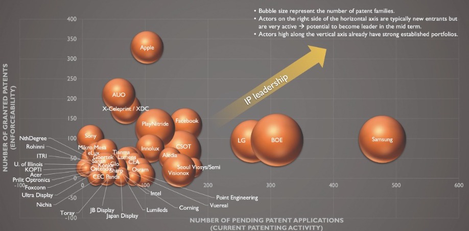
Yole has mapped out the competitive landscape in microLED IP. Source: MicroLED Displays – Intellectual Lanscape and Analysis report, Yole, 2021
The photonic crystal, surface-emitting laser combines a low cost with high speed and plenty of power
BY RICHARD TAYLOR FROM VECTOR PHOTONICS
SEMICONDUCTOR LASERS are revolutionising our
lives. These tiny emitters are now critical components
in data communications; additive manufacturing,
including metal and plastic printing; LiDAR; and
optical sensing – these are the world’s fastest growing
technology markets right now.
Helping to drive deployment in all these sectors is our team at Vector Photonics. Formed last year as a spin-out from one of the world’s leading photonic groups based at the University of Glasgow, we have invented the PCSEL, short for the Photonic Crystal Surface-Emitting Laser. This novel device, employing proprietary technology, is the first major breakthrough in semiconductor lasers since the commercialisation of the VCSEL in the 1990s.
The PCSEL’s greatest asset is that it combines a low cost with high speed and plenty of power. All other laser technologies fall short in this regard, offering no more than two of these three key characteristics.
As well as excelling on all those fronts, the PCSEL provides additional advantages. Like a VCSEL, it emits light from its top surface, making this laser easy to package and incorporate into a PCB or electronic assembly. However, its manufacture is similar to that of an edge-emitting laser, allowing production to draw on existing supply chain capability and capacity. And last but by no means least, the PCSEL spans a vast spectral range, equipping it with the potential to address a wide range of applications.
To drive the adoption of the PCSEL, we are continuing to develop and improve manufacturing techniques
for this class of laser. These efforts will help to broaden the PCSEL’s range of applications. Our initial focus
is on the datacom market, where this new class of laser appears to be the only technology capable
of meeting the requirements for next-generation,
high data rates. However, we are also starting to investigate plastic and metal printing applications, and it will not be long before we will also consider opportunities associated with mobile consumer and sensing applications.
To fully appreciate the merits of our invention, it is crucial to understand the production process of the established rivals, and how they operate.
The edge-emitting laser is capable of high-speeds and plenty of power, but it is expensive to make. In its simplest form – that is, the Fabry-Pérot laser, the original semiconductor laser technology – laser feedback and emission are both in-plane, causing light to exit the end of the laser, with gain reflection coming from facet mirrors. A variant of this design is the distributed feedback laser; it also features in-plane feedback and emission, but this time gain reflection comes from a grating structure.
The VCSEL has a radically different architecture, with mirrors above and below the active region providing out-of-plane gain and emission. Thanks to this, it is much cheaper to test and package this class of laser than an edge emitter.
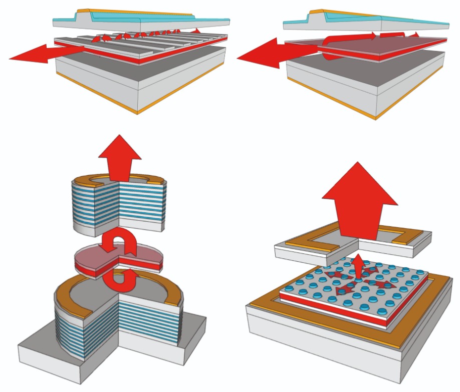
The PCSEL marries the best features of the edge-emitting laser, whether that be a Fabry-Pérot design (top left) or one that features a grating (top right), with the VCSEL (bottom left). Merits of the PCSEL include high powers, high speed and low costs.
Increasing the emission wavelength of the VCSEL is not easy. There is more to it than simply increasing the thickness of every layer within the Bragg stack. At longer wavelengths, the two materials used to form this structure tend to have a smaller difference in refractive index, so more periods are needed to ensure sufficient reflectivity. As well as increasing epitaxial growth times and cost, thicker stacks increase the resistance of the laser, and ultimately limit its output power. With these manufacturing challenges at play, it is not surprising that the VCSEL has a limited range of operational wavelengths. Note that for InP, the material associated with datacoms and telecoms wavelengths, there are no suitable pairs of lattice-matched compounds with a high index contrast.
The PCSEL does not suffer the same fate as it can be made from any direct bandgap semiconductor material system. What’s more, it enjoys the best of both worlds, combining in-plane feedback with out-of-plane surface emission, while benefiting from cheap test and packaging, just like a VCSEL.
An additional strength of the PCSEL over the VCSEL – and also any edge-emitter with a facet coating, such as that employed in a distributed feedback laser – is that it has a two-dimensional grating that is easy to scale. Compared to the VCSEL, the PCSEL also has other virtues: it has low contact resistance, ensuring the highest power output of any laser, size for size; and unlike a VCSEL, it does not contain an oxide aperture, so its production does not require specialist oxidation furnaces. And yet another merit is that its output is single mode, so scales up proportionally with area, due to the two-dimensional design and in-plane feedback.
Targeting datacom and telecom
Due to the absence of the InP VCSEL, the edge-emitting cousin serves this market. It can provide emission at 1310 nm and 1550 nm, the wavelengths offering optimal transmission for datacom and telecom, respectively.
Datacom networks use sources at 1310 nm, a wavelength that provides minimal dispersion in a single-mode fibre-optic cable. Minimising dispersion ensures that when transmitting a pulse of light through a fibre, it arrives at its destination at mostly the same time and relatively intact. This state of affairs is highly valued, because an intrinsically low dispersion during transmission diminishes demand for the coherence of the semiconductor laser. Incidentally, there’s no free lunch – the price to pay is greater attenuation in the cable, restricting the use of 1310 nm lasers to the relatively short distances used on datacoms applications. With the PCSEL, thanks to its high output powers, the transmission distances are not as short as they are for edge-emitting lasers.
Due to the far longer transmission distances for telecom – light might propagate 200 km before reamplification – the lasers that are employed emit at 1550 nm, where loss in the fibre optic cable is at its minimum. The trade-off is greater dispersion, so a laser needs to have a high degree of coherence to ensure good system receiver performance. The good news is that the PCSEL excels in this regard.

Table 1. The small mode volume for the PCSEL allow this class of laser to operate at high data rates than edge-emitting lasers and VCSELs.
Breaking the shackles is the PCSEL, which combines the mode width and length of the VCSEL with the mode height of an edge-emitting laser. Thanks to good mode confinement in all three directions, a PCSEL can be up to two-and-a-half times faster than a VCSEL with an equivalent emission area, and more than three times faster than a high-speed, edge-emitting laser (see Table 1).
Multiple opportunities
Another attribute of the PCSEL architecture is that it allows the fabrication of coherently coupled arrays, opening the door to several other opportunities. To produce this form of light source, laser elements of the array are joined by a coupler region. This links the in-plane light between laser elements, creating coherence. Using lenses, this coherent emission can be focused down to a small spot with a greater power density, an asset for cutting, welding, melting, engraving and drying applications.
As the laser elements of the array are coupled in plane, in an ‘n x n’ array, there is an obvious path to power scaling. The PCSEL realises high brightness, and thanks to its unique geometry, it can deliver kilowatts of coherent power. This is an accomplishment that cannot be replicated with other laser technologies.
Arrays also provide other valuable characteristics. By electronically tuning the phase of the coupler region to create an optical phased array, the beam produced by the laser can be steered, in real time, without moving parts. This attribute makes the PCSEL applicable to rapidly evolving LiDAR applications, which require steering of the beam for imaging. Other applications that could be revolutionised by the PCSEL include 3D printing in metal and plastic. Today these applications are served by systems involving a high degree of mechanisation. Switch to a solid-state solution based on a PSCEL and system size could shrink by a factor of ten while increasing reliability.
With the attributes that will allow it to serve in numerous applications, there is no doubt that the PCSEL is going to revolutionise semiconductor laser technology. Offering a great set of cherished attributes – it has a lower cost, greater speed and a higher, coherent power than all other current semiconductor laser platforms – its future is for the taking.
As SiC substrates sales soar, Cree’s Wolfspeed division is ramping capacity to maintain a vice-like grip on this market. Offering insight into how to scale, the art of crystal growth and massive expansion plans
CEO GREGG LOWE TALKS TO RICHARD STEVENSON
RS: Elon Musk, vying with Jeff Bezos for the moniker of the richest man in the world, has made his fortune through the soaring share price of Tesla, the pioneer of electric vehicles that employ SiC power devices. With the future for Tesla now looking brighter than ever, can we expect sales of SiC substrates to outpace recent predictions?
GL: The adoption of EVs and the drive for more efficiency, whether its electric vehicles or industrial systems, is definitely driving an increased adoption rate for silicon carbide. We’re in the early stage of a transition in semiconductors that happens only once every fifty years. That’s a transition from a silicon substrate to a silicon carbide substrate. The last time the semiconductor industry saw such a dramatic change was when digital designers went from bipolar transistors to CMOS.
RS: Aside from power electronics for electric vehicles, what do you see as the big markets where SiC substrates have a role to play?
GL: We recently announced two sets of products: back in April last year a 650 volt MOSFET product; and more recently, a month or so ago, a 1200 volt product. We are seeing tremendous interest in industrial markets for those types of products, things like solid-state circuit breakers, grid-connected devices, medical instruments. We are seeing adoption and interest in, just as an example, industrial blenders – think of them as mixers for chemical and industrial-type products, where power efficiency is really key. It’s a similar situation in server farms. Power is a tremendous on-going cost, and reducing that cost by using more efficient systems is key.
With the 650 volt MOSFET product that we launched, we had over 7,000 different applications from companies that said “I would be in interested in using this.” Altogether, that was a billion dollars of opportunity. This is standard in the analogue industry, where you see lots of different applications. We are very excited about those markets.
RS: Historically, Cree manufactured its LEDs on silicon carbide, but it has been moving over to sapphire. Does the sale of the LED products business unit, Cree LED, to Smart Global Holdings, signify the end of LED manufacture on silicon carbide substrates?
GL: The transition from a silicon carbide substrate to a sapphire substrate started a couple of years ago. The acquisition of our LED business by Smart Global will certainly continue that transition. Eventually, [Smart Global] will take the LED business and make it largely a sapphire business.
What we are doing is taking the capacity we allocated for LEDs and silicon carbide and converting our capacity to a Wolfspeed business. You will see the transition of LEDs from silicon carbide to sapphire, and with the selling of the business, it will move to an outsourced model as well. We will focus all of our silicon carbide business on the Wolfspeed business – power, and the RF business.
RS: Cree has been involved in high-profile wafer supply agreements, such as those signed with STMicroelectronics and Infineon. Do you see more agreements being signed, or have supply constraints eased?
GL: The demand for silicon carbide continues to outpace supply. We’re on a billion-dollar expansion capacity, both at the wafer fab level and the silicon carbide substrate manufacturing level. Our goal is to increase our manufacturing output by 30 times from the baseline of 2017.
We’ve recently announced the second expansion and extension of our supply agreements. The first expansion and extension was with ST; we’ve announced the second expansion and extension, another $250 million deal.
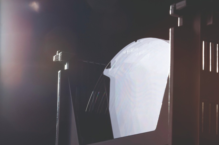
Wolfspeed is ramping substrate production through the installation of new tools.
I think the fact we have a fairly substantial percentage share [of the SiC substrate market], and that we are investing a tremendous amount of capex in expanding our manufacturing footprint, continues to drive customers our way, in terms of them looking for assurance of supply of silicon carbide substrates.
RS: What proportion of Cree’s substrates are used internally?
GL: We don’t split that out exactly, but between our device business and our silicon carbide business, roughly half is devices and roughly half is silicon carbide substrates. Over the coming years we would anticipate that our device business and our silicon carbide substrate business will grow, but the device business will likely grow faster than the substrate business.
RS: Cree is in the midst of an expansion, with a ramp in silicon carbide production in Durham, and construction of a wafer fab in Mohawk Valley. Is the plan to use both sites for the production of silicon carbide substrates?
GL: Currently we’re planning an expansion of our silicon carbide manufacturing capability in Durham, North Carolina. We have a second site basically across the street from our first site.

Tesla is helping to accelerate sales of SiC power devices.
The team working on the New York wafer fab has made tremendous progress, despite starting when Covid was just starting to devastate the U.S. We began the expansion and despite [the pandemic] the team has done a great job of staying on track. It will be the world’s largest silicon carbide wafer fab and the world’s first 200 millimetre-capable silicon carbide wafer fab.
RS: To increase silicon carbide substrate production there needs to be investment in more growth equipment and the introduction of more technicians to run these tools. Crystal growth is viewed by some as a black art, with experience critical. Is that your view, or is it a process that new technicians can master in a few months?
GL: It definitely takes a lot of experience. If you look at our experience in silicon carbide crystal growth, it spans three decades. Some of the folks that are working on the 200 millimetre project worked on quarter-inch silicon carbide crystals.
As we move from 150 to 200, you are talking about a new process to grow the crystals, new machines to grow the crystals – we actually build those machines ourselves – and the methodology to extract crystals with very low defect densities. That’s not easy to do. It remains an area that has tremendous barriers to entry.
Silicon carbide grows at a very, very high temperature, on the order of 2500 Celsius. You don’t start the process and then open it up halfway through to see how it’s going. You have to know what you’re doing before you get the machines ramped up to those kinds of temperatures. Even process monitoring, temperature monitoring, the way you do cooling, all of that is super-important to the quality of the crystal. And a lot of that is stored in the brains and the knowledge of our team. You can’t go down the street and buy a silicon carbide growth machine.
RS: My impression is that SiC substrate quality has increased, and there is less concern related to the various types of defect that can plague this material. When scaling to 200 millimetre silicon carbide, does much effort have to be devoted to ensuring that these imperfections continue to be minimal?
GL: Absolutely. There is a tremendous amount of effort on that. When we got out the first 200 millimetre wafers, we realized we had a lot of work to do on dislocations and defects. But the team has done a tremendous amount of work on that.
You also have stresses that are induced. Typically, in the case of silicon carbide, crystal growth is hard because of the temperature you are working with. But the stresses increase as you increase the diameter, which impacts wafer shape – and that’s a big deal for the ability to use a wafer in a wafer fab.
Even at 150 millimetre, there has been an increase in quality. We’ve certainly be leading the charge on that – there is a need for increased quality at 150 millimetre. The adoption of silicon carbide in high-power markets, including automotive, industrial, grid applications, etc., is driving the increase in die size of silicon carbide chips. The increased size of the chips makes it more important that the defect density is lower, because the probability you have a defect in a bigger chip is higher. So there is improving quality that is tracking very closely the requirement for the improvement, and the demand for the improvement, but based on the size and the amount of power that customers are looking to get out of these chips.
RS: How does Cree ensure consistent, high-quality product? What do you do to monitor the quality of your substrates?
GL: We use a lot of product internally in our wafer fabs and that gives us immediate, very short-cycle-time feedback to our crystal growth team, in terms of improving quality and capability of the device, the substrate, of the epistructure, etc.
We also work very closely with our partners, like ST. They give us feedback as well. Customer feedback is the greatest way to know if you are making improvements. We feel pretty good about the feedback we are getting, in terms of the improvements we have made on the silicon carbide substrates, and then the epi capability as well.
RS: Where is Cree now, in terms of the ratio of its 100 millimetre and 150 millimetre production of SiC?
GL: We have made a pretty significant transition from 100 to 150. It’s in excess of 75 percent of our production. I would anticipate that the 100 millimetre will fade as a percentage of the business as we increase our capability at 150, and transition some of that capability to 200 millimetre.
RS: It seems that for silicon chip production, there is a sweet spot associated with the 300 millimetre wafer. 450 millimetre production is possible, but the benefits don’t seem to warrant the outlay. With GaAs, production has now been at 150 millimetre for more than a decade. With SiC, will 200 millimetre be the optimum?
GL: What I will tell you is that we feel very good about the transition we are making from 100 to 150, and then the introduction of 200 with the Mohawk Valley fab.
I think we’re in a transition to 200 millimetre for the next decade. If there is another wafer diameter beyond that, we’re probably talking about at the earliest, the end of this decade. That does track what normally happens in semiconductors. It’s a relatively high capital-intensive business. Companies build a 200 millimetre fab and then want to run it for at least a decade before they start converting it, so it matches the normal transition of wafer fabs.
RS: What gives Cree an edge over its rivals in the SiC substrate market. Is it the volume of supply, the quality of the product, or the pricing?
GL: I think it starts with a tremendous amount of experience – we have thirty years of experience with this technology. That experience translates into high quality; the high quality gets us access to customers and markets, which drives our scale up; the increase in scale allows us to have more learning cycles; more learning cycles helps us improve our yield and drive our costs down; and as we drive our costs down we’re are able to sign up more customers, which increases our scale, gives us more learning cycles.... you get the point, we’ve created a bit of a flywheel.
The long-term supply agreement customers – which includes, from an announcement perspective, ST, Infineon and ON Semiconductor – allow us to continue to drive costs down.
It has been a really important factor to utilize scale to drive improvements in productivity, yield, quality etc., to drive cost down. We need to get the price differential between silicon to silicon carbide lower and lower and lower. I think we’ve been able to achieve that over the last couple of years.
RS: You’ve recently announced that you’ve changed the name to Wolfspeed Cree. What’s the thinking behind that move?
GL: The company has a tremendous amount of legacy and capability and brand awareness as an LED and lighting company. That’s largely around the brand Cree. Now that we’ve sold the LED business, we really are a compound semiconductor company focused on power and RF chips, and silicon carbide substrates with gallium nitride capability as well.
The Wolfspeed brand has been out there for the last five years. It’s well known and well respected as that part of Cree that is the power and RF semiconductor part. So we felt this was the perfect time, as we close the sale of the LED business to Smart Global, to transition the name of the company to replicate what we’ve really become. The fact that we had the brand out there has given us the opportunity to do this.
We’re not creating a new brand, we are just simply saying that we are focusing on these businesses, no longer LED or lighting. It’s a great opportunity for us to highlight the focus of the company in these areas.
Speakers at Photonics West outlined a variety of options for improving the performance of the deep-UV LED
BY RICHARD STEVENSON
HOW DO YOU VIEW the deep-UV LED? It’s easy to see this source as only a killer of viruses, and in particular Covid-19, now that the pandemic has been dominating our thoughts for more than a year. But the opportunities for this class of LED extend well beyond the purification of air, water and surfaces. This chip can also lie at the heart of systems sensing a range of gases, and provide the light source for non-line-of-sight communication.
For all these applications, the deep-UV LED has its pros and cons. Unlike the more traditional sources of emission in this spectral domain – the excimer lamps, and those based on the likes of mercury, deuterium and xenon – it is not fragile, bulky, or suffering for a short lifetime. But it’s wall-plug efficiency is pitiful, trailing that of its blue cousin by a substantial margin, particularly when emission ducks below 250 nm.
With the deep-UV LED, there are so many barriers to a better performance. However, look at this situation in a more positive light, and you’ll see that there are also so many opportunities to propel the performance to a new level. These options, discussed in detail at this year’s SPIE Photonics West, include: reducing the defect density in the foundation, to prevent the active region from being riddled with a high degree of imperfections; increasing the internal quantum efficiency by improving the architecture of the light-emitting region; and delivering a hike in the proportion of light that exits the chip.
Which foundation?
A compromise is inevitable when selecting the foundation for the deep-UV LED. Bulk AlN minimises the defect density in the heterostructure, but it is pricey and availability limited. Consequently, developers and manufacturers of deep-UV LEDs tend to use a sapphire substrate, and employ growth technologies to drive down the defect densities in the epistructure. Quash defect densities as low as 108 cm-2 and internal quantum efficiency as high as 80-90 percent should be possible, assuming the absence of non-radiative defects.
Over the last few years Michael Kneissl’s group from TU Berlin, Germany, have been working in collaboration within researchers at FBH to increase the material quality in AlN films grown on sapphire. Kneissl, who gave an invited talk at this year’s Photonics West, explained that his group initially focused on growing a thin AlN film on sapphire, etching columns through the nitride and into the substrate, and applying overgrowth that caused AlN to coalesce. However, while this approach formed good films with a thickness of 5.5 μm, it was not ideal. “Patterning is time consuming and costly,” admitted Kneissl.
More recently, his team has turned to a low-cost approach pioneered by Hideto Miyake’s group at Mie University, Japan. This method involves sputtering AlN on sapphire, before annealing the resulting template under nitrogen gas at 1700 °C. “After this three-hour anneal we observe a very significant reduction in threading dislocation density in the AlN layer,” explained Kneissl. These templates have a good morphology, with a threading dislocation density of 7.2 X 108 cm-2 realised in a 350 nm-thick film.
The latest approach by Kneissl and co-workers is to combine both techniques, forming an AlN-on-sapphire foundation by sputtering, annealing and overgrowth. This promises to lead to even lower dislocation densities. Results are encouraging, with samples produced by high-temperature annealing and epitaxial overgrowth providing the highest values for the internal quantum efficiency. Measurements suggest a value of almost 30 percent.
Kneissl said that encapsulated LEDs produced on this template emit at 265 nm, are capable of producing 54 mW at 350 mA, and have a peak external quantum efficiency of 3.7 percent. He believes that far higher values could be realised through the introduction of reflective contacts and a transparent p-side.
Facing together
The trailblazer of the sputtering and annealing approach, Miyake, also spoke at this year’s Photonics West. His team form high-quality templates by sputtering AlN on sapphire and then taking pairs of AlN-on-sapphire epiwafers, placing their growth faces together, and annealing them under nitrogen at 1 atmosphere for between 10 minutes and 10 hours. “Typically we use 3 hours,” added Miyake.
To illustrate the dramatic improvement in crystalline quality wrought by annealing, Miyake presented X-ray diffraction data showing that the elevated temperature delivered a dramatic reduction in the diffraction peak width from 532 arcsec to 49 arcsec.
Efforts to optimise the sputtering conditions have included evaluation of the impact of sputtering pressure, layer thickness and annealing temperature. These experiments showed that when annealing films at 1700 °C for 3 hours, a lower sputtering pressure reduces the chances that cracks form. Reduce the sputtering pressure to just 0.03 Pa and it is possible to produce crack-free films more than 800 nm-thick. When it comes to optimising crystalline quality, the sputtering pressure influences the ideal thickness. For example, when growing at a sputtering pressure of 0.03 Pa, measurements of X-ray diffraction indicate that the ideal AlN thickness is around 700 nm.
It is not easy to select the optimum annealing temperature, as several factors are at play. A study involving a series of 480 nm-thick AlN films, grown at a sputtering pressure of 0.05 Pa and temperatures ranging from 1650 °C to 1775 °C, revealed that higher temperatures had no impact on the width of the X-ray diffraction peak in the (0002) direction. However, for the (10-12) direction, the peak’s full-width at half maximum fell fr om over 170 arcsec to below 125 arcsec. Note, though, that this gain comes at the price of an increase in macroscopic defects. To minimise these imperfections, an alternative to dialling back the annealing temperature is to turn to a thicker film.
The benefits of a thicker film are quantified by plan-view scanning transmission electron microscopy images of a portfolio of sputtered films annealed at 1700 °C. For these samples, capped with an AlN layer between 0.8-2.8 μm thick that’s been added by MOCVD, threading dislocation density falls from 1.1 x 109 cm-2 to 3.6 x 108 cm-2 when the thickness of the sputtered film is increased from 153 nm to 481 nm.
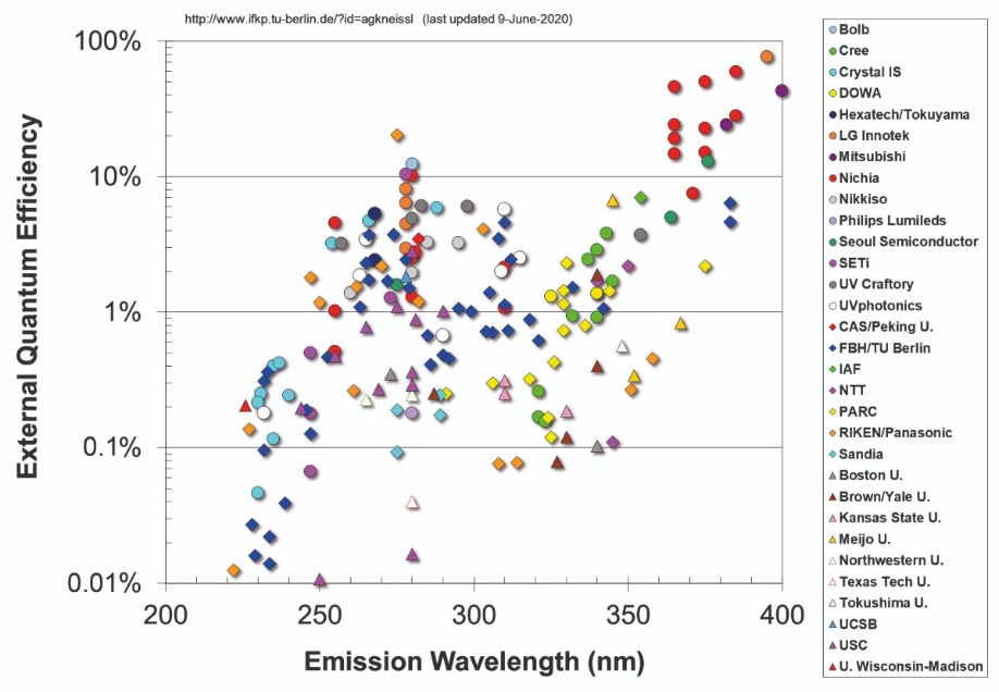
Figure 1. As the wavelength of the UV decreases, there is a tendency for the external quantum efficiency to fall. This plot is provided by Michael Kneissl from TU Berlin. It is an updated version of Figure 2 from the paper M. Kneissl et al. Nature Photonics 13 233 (2019)
The team has also compared the characteristics of AlN films grown directly on sapphire by MOCVD, and those added by MOCVD to AlN-on-sapphire templates formed by sputtering and annealing. The latter leads to a far lower screw and mixed dislocation density – it is 2 x 106 cm-2, rather than 3 x 108 cm-2.
While this lower density may appear a blessing at first glance, it brings its own problems. This is evident when comparing Nomarski microscope images of 1500 nm-thick films of Al0.74Ga0.26N grown by MOCVD on top of both structures. A relatively smooth surface results when this alloy is deposited on MOCVD-grown AlN-on-sapphire, but when it is grown on a template of sputtered and annealed AlN that has a layer of MOCVD grown AlN, the AlGaN is riddled with huge hillocks.
Miyake and co-workers have found that the origin of these hillocks is the spiral growth in the sputtered AlN templates. Due to the low density of screw and mixed-type dislocations, hillocks grow without interruption to a large size. In stark contrast, when there are many more screw and mixed type dislocations – this is the case in the epistructure featuring AlN growth on sapphire by MOCVD – there is interference associated with dislocation-induced spiral growth that creates a flatter surface (as illustrated in Figure 2).

Figure 2. The low density of screw and mixed-type dislocations in high-quality AlN of sapphire templates are behind the large hillocks that form during MOCVD growth. When more screw and mixed-type dislocations are present, they interrupt the formation of hillocks, reducing their size. This graphic has provided by Hideto Miyake from Mie University. More details are given in the following papers: H. Miyake et al. J. Cryst. Growth 456 155 (2016); S. Xiao et al. J. Cryst. Growth 502 41 (2018); K. Uesegi et al. Appl. Phys. Express 12 065501 (2019).
To assess the impact of the offcut angle on the quality of the active region, the team from Mie University carried out a cathodoluminescence study on samples featuring quantum wells. Increasing the off-cut angle to 0.6° led to a more intense, narrower photoluminescence peak. But further increases in off-cut angle were not beneficial, resulting in a lower intensity of emission. “We speculate that this behaviour is owing to surface step bunching, and results in degradation of the multi-quantum wells,” argued Uesugi.
The researchers have considered various options for combatting the hillocks. Increasing the temperature eradicates them, but introduces point defects. A better option is to combine a lower growth rate with a high ammonia partial pressure, a step that suppresses excessive surface migration of gallium atoms. Drawing on all these tricks, the team have produced deep-UV LEDs on sapphire with a 0.6° offcut. MOCVD-grown layers were added in a Taiyo Nippon Sanso reactor, using a growth temperature of 1300 °C for the first AlN layer, before dropping the temperature to 1150 °C to grow the device layers.
On-wafer measurements on circular, un-encapsulated 264 nm devices with 160 μm diameter revealed a maximum external quantum efficiency of 1.73 percent. When driven at 20 mA, output is 1.61 mW. In comparison, the control, made on MOCVD-grown AlN, has a maximum external quantum efficiency of just over 1.4 percent.
Ultrathin wells
It is well known that the internal quantum efficiency of the active region of an LED is governed by the interplay between non-radiative and radiative processes. As the emission wavelength heads deeper into the UV, there is a decrease in the photoluminescence lifetime, which is the reciprocal of the non-radiative lifetime. This implies that non-radiative recombination increases at shorter wavelengths.
Working at Kyoto University, Japan, Mitsuru Funato and co-workers have measured the photoluminescence lifetime of quantum-well samples emitting at a range of wavelengths, formed on both sapphire and bulk AlN. Funato told delegates at Photonics West that despite these two classes of sample having markedly different threading defect densities, lifetimes are similar. This led him to believe that the major non-radiative recombination centres are point defects, rather than threading dislocations.
Many years ago, theorists calculated the formation energy for point defects in GaN and AlN. Based on these works, Funato is suggesting that the weakness in the AlGaN quantum wells is the point defect associated with aluminium. He is advocating the use of gallium-rich AlGaN quantum wells. There is much merit to this approach: the optical anisotropy in AlGaN hampers surface emission, which is strong in GaN, aiding light extraction efficiency.
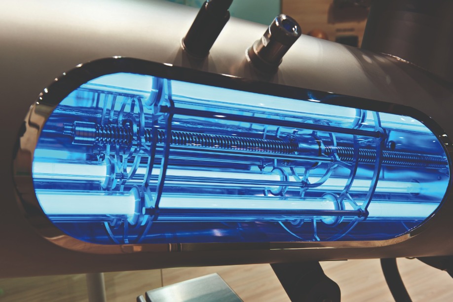
UV lamps are widely used for water purification, but as UV LEDs improve, they will take an increasing share of this market.
Encouraged by this result, the researchers have gone on to grow ultra-thin GaN quantum wells. They are not the first to do this, but previous work has focused on an MBE-based approach. The team from Kyoto use MOCVD, realising very thin GaN quantum wells with a self-limiting process. Funato told the delegates at Photonics West that he thinks that the first monolayer of GaN stabilises on AlN, but when a second monolayer is added, it evaporates. The upshot is that the thickness of the quantum well is limited to a monolayer, thanks to a bond strength for GaN-on-AlN exceeding that for GaN-on-GaN. Evidence for such a thin well has come from a transmission electron microscopy cross-sectional high-resolution image that show a single monolayer of GaN sandwiched between AlN.
Photoluminescence measurements at a range of temperatures up to 300K have produced promising results. Temperature quenching is less suppressed in the GaN quantum well emitting at 300 nm than its thicker AlGaN cousin, implying a higher internal quantum efficiency. A room-temperature value of 5 percent is estimated for the GaN well, compared with 0.1 percent for the AlGaN variant.
Turning to time-resolved photoluminescence at room temperature has provided additional insight into the nature of the wells. The photoluminescence lifetime is 40 ps in the 1.5 nm-thick AlGaN quantum well, while it is 100 ps in the single monolayer GaN well, indicating that the latter is better at supressing non-radiative processes.
Funato and colleagues have also carried out time-resolved photoluminescence at cryogenic temperatures. Armed with these additional measurements, they have deduced radiative and non-radiative lifetimes. In AlGaN both lifetimes are 0 ps, while in GaN the non-radiative lifetime is 105 ps and the radiative lifetime just 2 ns, due to larger electron-hole overlap.
The team has investigated the emission’s polarisation state by exciting the sample head-on with a 193 nm laser and measuring emission in-plane with a CCD. The researchers found that the transverse magnetic polarisation is slightly stronger than the transverse electric form in the AlGaN quantum well, while the transverse electric dominates in the GaN quantum well, aiding light extraction.
To try and reach even higher values of internal quantum efficiency for ultra-thin GaN quantum wells, the team have switched to the semi-polar plane. A two monolayer-thick GaN quantum well formed on r-plane of sapphire and emitting at around 250 nm produced an internal quantum efficiency of 50 percent.
Deep UV dots
Another option for producing a deep-UV active region, outlined in a presentation by Julien Brault from CNRS-CRHEA in France, is to use AlGaN quantum dots. As these nanostructures provide a high level of spatial confinement for electrons and holes, there is the promise of realisation of a high quantum efficiency in samples with a relatively high defect density.
Working with reearchers at the University of Montpellier and Riber, Brault and his colleagues have produced and studied quantum dot samples that are grown by MBE using the Stranski-Krastanov growth mode. One of the primary goals of this research is to determine the growth condition for realising dots with high internal quantum efficiency.
This collaboration forms its dots on sapphire substrates coated with an AlN layer typically 1 μm thick. This template has a dislocation density of the order of 5 x 1010 cm-2. AlGaN dots with an aluminium component of 10-40 percent are grown on Al0.7Ga0.3N, which is also used to clad them. Cross-sectional transmission electron microscopy of these dots, which have a density in the range 3-6 x 1011 cm-2, reveals that the nanostructures are between 1.5 nm and 3 nm high, and have a diameter of around 10 nm.
Brault shared atomic force microscopy images showing that post-growth annealing, at temperatures greater than 800 °C, induces a shift in the shape of the quantum dots from elongated structures to symmetric entities. The change in morphology has no impact on the emission wavelength, implying no change in AlGaN composition. However, there is a tremendous ramp in room-temperature photoluminescence efficiency from 1-3 percent to 10-30 percent, attributed to a significant increase in carrier confinement.
The researchers used time-resolved photoluminescence to investigate the internal quantum efficiency of dots with aluminium components between 10 percent and 40 percent – they span the spectral range 340 nm to 275 nm. The team found that as the wavelength gets shorter, the internal quantum efficiency increases, to around 20 percent in the UVC.
Building on this work, Brault and colleagues gone on to produce LEDs that feature these nanostructures. The devices, sporting a relatively standard structure, have three-to-five quantum dot planes and a p-type GaN contact layer. The latter improves hole concentrations, but increases absorption in the UV range.
The French collaboration has fabricated UVA LEDs with Al0.1Ga0.9N quantum dots, UVB siblings with Al0.2Ga0.8N quantum dots, and expects to reach between 265 nm and 280 nm by increasing the aluminium component to 0.3 to 0.4.
Behaviour of these emitters is quite unlike that of a conventional LED, with performance highly current dependent. When carriers start to flow through the device, initially there is a dramatic decrease in emission wavelength, alongside a reduction in the width of the emission peak. Both trends are believed to stem from fluctuation in the composition and size of the dots, and a screening effect. Further increases in current lead to a second regime, where the emission wavelength stabilises and its peak narrows. It is thought that these characteristics are associated with the injection of carriers into Al0.2Ga0.8N quantum dots. Crank the current up even more and there is an increase in emission wavelength, due to thermal effects, and a reduction in injection efficiency.
These quantum-dot devices have an operating voltage of 10-20 V. External quantum efficiency peaks at just below 0.1 percent, with heating causing this figure to fall.
“The next step will be to fabricate tunnel-junction-based LEDs, where we can expect a strong improvement in the internal efficiency and the extraction efficiency, by avoiding the use of a p-type GaN contact layer,” said Brault.
Extracting emission
One of the biggest weaknesses with a conventional deep-UV LED is its low extraction efficiency. Hideki Hirayama from Riken University, Japan, highlighted this impediment in his talk, before discussing a variety of architectures that can address this issue.
According to Hirayama, for a standard UVC LED, extraction efficiency can be as low as just 4-8 percent, due to a p-GaN contact that absorbs light and internal reflections in the sapphire substrate. He explained that one option for getting more light out of the chip is to add a photonic crystal structure on the n-side of the device, but this only increases the extraction efficiency to 12-15 percent. A far better strategy, he said, is to address the weaknesses of the p-side, by switching to a highly reflective electrode and a transparent contact layer. Combine this with a pillar-based technology on the n-side of the device – claimed to be a better option than a photonic crystal structure for boosting extraction from the n-side – and light extraction efficiency could exceed 70 percent.
Hirayama and co-workers produce their UVC LEDs on sapphire, beginning with the growth of a five-step multilayer buffer, created by ammonia pulse flow growth. This 3.8 μm-thick structure, which has a dislocation density of 5 x 108 cm-2, has provided the foundation for producing a portfolio of UVA-UVC LEDs. Devices emitting at 270 nm produce an output of more than 50 mW. Internal quantum efficiency is estimated to be 54 percent, according to photoluminescence measurements made at a variety of temperatures. The team has devoted several years to developing approaches to increasing the light extraction efficiency of deep-UV LEDs. Back in 2017, these researchers reported results for devices featuring: transparent p-AlGaN layers, a reflective p-type electrode, an AlN buffer on patterned sapphire, and a lens-like resin mold. This powerful combination yielded a world-record light-extraction efficiency of 20.3 percent for a 275 nm LED, according to Hirayama.
While this is impressive, Hirayama is quick to point out that more work is needed, given that the wall-plug efficiency is only around 6 percent. Losses can be attributed to the use of p-AlGaN, which leads to a hike in the operating voltage – it increases from around 5.5 V to 9.1 V. Recently, the team evaluated the benefits of inserting a photonic crystal reflector in the p-side of the LED. Simulations suggest a three-fold enhancement in light-extraction efficiency – this could hit 54 percent, when pairing this novel reflector with p-type AlGaN.
Hirayama and co-workers have produced photonic crystal UV LEDs by nano-imprinting and dry etching. These devices, containing an array of holes with a 160 nm diameter and depth of 338 nm in the p-side, alongside a highly reflective mirror made from the combination of nickel and magnesium, operate with an external quantum efficiency of up to 10 percent.
To reduce the operating voltage, the team has also produced variants with p-type GaN. Introducing the photonic crystal is beneficial, as it doesn’t alter current-voltage characteristics, but enhances light extraction by 70 percent. That’s not as big a gain as promised by simulations, because the photonic crystal is yet to be optimised. The latest generation of UVC devices produce between 30 mW and 50 mW.
Even higher powers are produced by large flip-chip structures. For devices 1.2 mm by 1.2 mm in size and driven at 2 A, output is as high as 140 mW.
The effort by Hirayama and co-workers, and those of other researchers in deep-UV LEDs presenting their successes at this year’s Photonics West, show that the performance gap between this device and its blue cousin is narrowing. The strategies are clear, and as implementation improves, these chips are sure to offer more bang for their buck.
Dielectric mirrors and an AlGaN membrane enable the VCSEL to dive deep within the UV
BY ÅSA HAGLUND FROM CHALMERS UNIVERSITY OF TECHNOLOGY
VCSELs are ubiquitous devices. Best known for providing data communication and facial recognition in smart gadgets, this class of laser, undergoing exponential growth, is also serving in several other applications. It is being deployed to monitor oxygen levels in combustion processes and in anesthetized patients in hospitals; and in the form of large-sized arrays, it is providing a source of heating in industry.
Today, commercial VCSELs only span the red and infrared. If emission were stretched down to the green, blue, and ultraviolet, this would allow this compact, power-efficient, low-cost source to target completely new markets, such as those involving flood lights, projectors, sterilization, and medical diagnosis and treatment.
Responding to the call is our team from Chalmers University of Technology, working in partnership with colleagues at the Institute of Solid State Physics, TU Berlin. Our most significant milestone to date has been the setting of a new benchmark for the world’s shortest wavelength VCSEL at 310 nm, using a new concept for UV emitters. Although our record has just been eclipsed by a partnership between researchers at Xiamen University and Advanced Micro-Fabrication Equipment Inc., their approach has variations in cavity thickness that are far, far larger than suitable for laser fabrication, leading us to believe that our success could still be the catalyst that kick-starts a new era for the VCSEL.
The importance of the UV...
Extending the VCSEL’s emission to the UV will open up many new markets. Some of them require the attributes of a laser – that’s the case for atomic clocks, and tuneable diode laser spectroscopy that provides high-resolution sensing of various gases, including O3, NO2, SO2 and NO. But there are also applications that simply need a source of speckle-free illumination with a more well-directed illumination pattern and a higher brightness than an LED array. These requirements, which could be met by two-dimensional VCSEL arrays, open up opportunities such as: the sterilization of bacteria and virus (including SARS-CoV-2) on surfaces, in liquids and in air; dermatological phototherapy; photolithography; material curing; greenhouse illumination; biosensing; fluorescence imaging; and medical diagnosis, analysis and treatment. Additional applications will also pop up once UV VCSELs are commercialized, just like they did for infrared VCSELs.
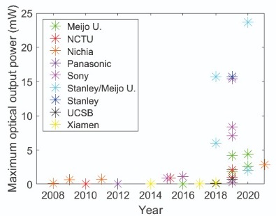
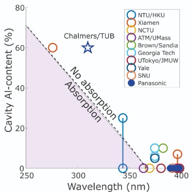
Figure 1. (a) Optical output power for continuous-wave, electrically injected blue VCSELs as a function of year. (b) The aluminium-composition in the cavity vs. lasing wavelength for realized UV VCSELs, where non-filled (filled) markers are optically (electrically) injected. The upper right half of the figure shows the region where UV VCSELs can be realized, i.e. cavities with a high enough aluminium-composition to avoid re-absorption of the intended emission wavelength.
Underpinning this breakthrough has been advances in thermal management, optical confinement, mirror reflectivity, and electrical injection.
It may seem that the development of UV VCSELs can draw on advances made in the blue. After all, both types of VCSEL are made from the III-nitride materials system. However, so far there have only been a handful of demonstrations of UV VCSELs, and they are predominantly optically pumped variants, emitting in the UVA spectral regime of 320 nm to 400 nm (see Figure 1(b)).
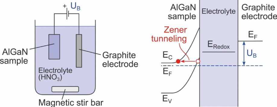
Figure 2. (a) Set-up for electrochemical etching of AlGaN. (b) Band bending and tunnelling when a positive potential is applied to AlGaN during electrochemical etching.
Our novel concept overcomes these restrictions. By allowing the use of high-aluminium compositions in the cavity, our method has enabled us to demonstrate the world’s first UVB-emitting VCSEL. As it also offers great potential for extension into the UVC, it promises a technology for realising VCSELs in the full UV spectrum from UVA to UVC.
...and the challenges
All VCSELs feature an optical gain region, consisting of a few quantum wells sandwiched between a pair of mirrors. For every round trip of the light, the gain path length is incredibly short, so the roundtrip losses must be very low to realise lasing – fail to minimise loss, and this will outweigh optical gain. The key to ensuring lasing is to produce mirrors with a very high reflectivity, typically more than 99 percent is required for well-performing VCSELs.
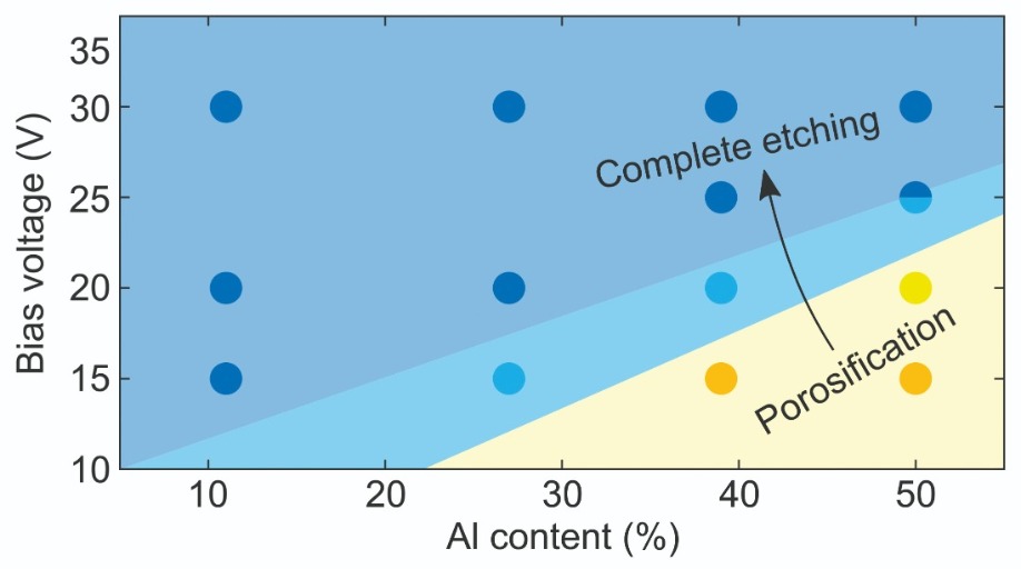
Figure 3. Different morphologies of the electrochemically etched AlGaN as a function of etch voltage and aluminium-composition.
Another challenge for developers of VCSELs is that due to the vertical cavity configuration, light must propagate in the same direction as that for injecting the current into the quantum wells. This condition compromises the location of the low-resistive ohmic contacts. They cannot be placed in the optical path, as they will then cause unacceptably high optical absorption. The common solution is to turn to ring-shaped contacts and rely on horizontal current spreading, preferably within the DBRs.
For infrared VCSELs, it’s not that difficult to address the challenges of high-reflectivity mirrors and current injection. Devices operating in this spectral range are blessed with an AlGaAs materials system that is lattice-matched and easy to dope. Thanks to these virtues, fabs have well-established processes for producing electrically conductive mirrors that provide a high reflectivity over a broadband.
With blue and UV VCSELs, the production process is not so easy. Within the III-nitride materials system there is no obvious choice for a lattice-matched combination of two materials that yield the high-refractive index difference needed to make a suitable DBR. What’s more, it is a challenge to produce highly electrically conductive layers with this material system, due to the high ionization energy of the dopants. Ionization energy increases with bandgap, and is highest for p-doped materials. Further complications come from large bandgap offsets, polarization fields and a strong imbalance between electron and hole mobilities – all hamper electrical injection.
Most of the effort at developing the UV VCSEL has been directed at the UVA, with work focused on developing good enough DBRs for demonstrating lasing in vertical cavities under optical pumping. There have also been many attempts to develop epitaxial DBRs for the shorter wavelengths in the UV, but so far no group has demonstrated a reflectivity above 99 percent in the UVB or UVC domain.

Figure 4. The process flow for a UV VCSEL with two dielectric DBRs. The formation of the laser is enabled by substrate removal through selective lateral etching of a sacrificial AlGaN layer.
Turning to electrochemical etching is one approach that can break the strong bonds in AlGaN and allow the oxidised material to be dissolved in an electrolyte. To carry out this form of etching, the sample must be electrically connected to an electrode and submerged in the electrolyte (see Figure 2). Applying a positive potential to the sample bends the bands, allows for Zener tunnelling, and thus generates holes in the n-doped AlGaN sacrificial layer. These holes accumulate near the semiconductor-electrolyte interface, and since they equate to broken bonds between group III and nitrogen atoms, result in oxidation of the AlGaN. Careful choice of the electrolyte ensures that the oxidized material is unstable, so dissolves.
For compositions richer in aluminium, a higher voltage is required for Zener tunnelling (as indicated in Figure 3 (a)). Another factor influencing electrochemical etching is the doping concentration, because layers with higher doping require a lower applied potential for tunnelling. Working with medium-range potentials, only slightly above what is required to achieve tunnelling, it is possible to realise porosification instead of complete etching of AlGaN. This porosification stems from local variations in the electric field strength, exacerbated at the tip of the etched pores. Porosification or complete etching can be used to create porous or airgap DBRs, where every second layer in the DBR should either have a higher doping concentration and/or a lower aluminium-composition than its surrounding layers.
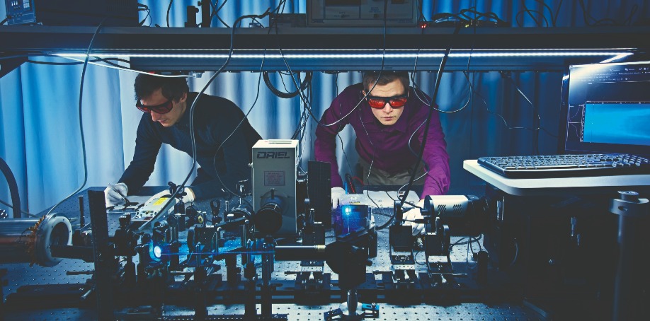
Characterization of UVB VCSELs by Filip Hjort and Joachim Ciers at Chalmers University of Technology.
A team at Yale University has recently reported progress in nanoporous AlGaN DBRs, and another at Georgia Tech recently detailed success with an airgap DBR, both implemented in full UV VCSEL structures. Both groups used a 5 percent aluminium composition in the DBR and targeted UVA emission. This work is in its infancy, and more research is needed to fully explore the benefits of porous and airgap DBRs; prove their homogeneity, mechanical and long-term stability; and propel them into the UVB and UVC by etching layers that are much more rich in aluminium.
We are pursuing an alternative approach to that of nanoporous or airgap DBRs. Our VCSELs feature a dielectric bottom DBR that provides mechanical and long-term stability. This approach has much promise, having already delivered success with blue and long-wavelength infrared VCSELs.
Producing VCSELs with a bottom dielectric DBR has its own challenges, which in most cases is the removal of the substrate (see Figure 4). This step must leave a very smooth surface, to ensure minimal optical scattering losses in the cavity; and it must be incredibly precise, because the exact cavity length determines both the spatial overlap between the standing optical field and the gain/loss regions, and the spectral matching between resonance and gain peak wavelength. In addition, the substrate removal process must not hamper the quality of the device layers.
Ideally, we would draw on techniques explored for substrate removal in AlGaN-based LEDs, such as laser-induced lift-off and chemical mechanical polishing. However, they are unsuitable for VCSELs, leading to either cracking of device layers and rough surfaces, or poor thickness control. All these issues can be avoided with an electrochemical etching approach that is suitable for AlGaN-layers with up to 50 percent aluminium-composition. This technique has been crucial to our demonstration of the world’s first UVB VCSEL.
Plummeting the depths
Our partners at TU Berlin have grown our VCSEL cavity, including the quantum wells and the sacrificial layer needed for substrate removal, by MOCVD. Their starting point was an Al0.55Ga0.45N pseudosubstrate provided by FBH. The sacrificial layer that we use is actually a highly n-doped multi-layered structure, chosen partly because it enables incorporation of lower aluminium-content layers while not degrading the crystal quality of the device layers. Another merit of this particular design is that the built-in polarization fields yield sheets with high carrier concentrations. Both factors enhance etch selectivity between the sacrificial layer and the cavity, and result in a smoother etched surface.
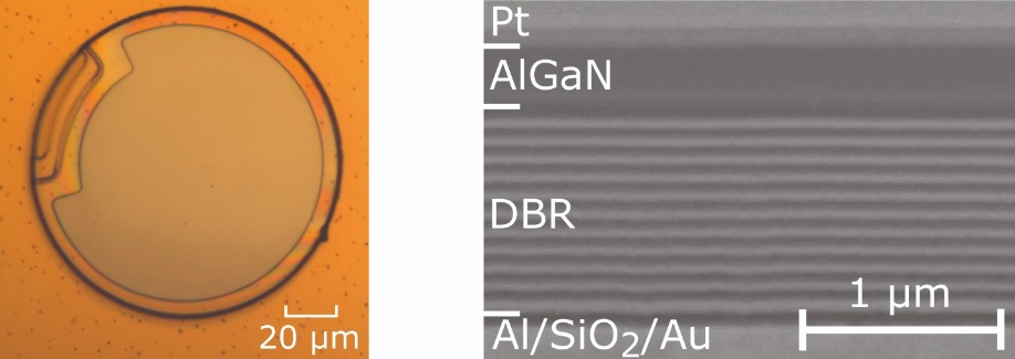
Figure 5. (Left) Top-view optical microscope image of a fully fabricated UVB VCSEL. (Right) Cross-sectional scanning electron microscopy image of a half-VCSEL with the highly reflective DBR and AlGaN cavity. The platinum on top is for protection of the topmost cavity layer during the focused ion beam cut. It is not present in the full VCSEL structure.
Aside from this aluminium layer, our structure is not specially designed for optical pumping. Instead, the architecture has been selected for future electrical injection. This means that there are no special layers for optimising the optical absorption of the pump, to ensure a high carrier concentration in the active region. There are just three thin quantum wells in the optical gain region, rather than multiple gain regions. By taking this approach, we will take a smaller step when we progress to an electrically injected device, because we will be using a VCSEL structure with an optical loss that is proven to be sufficiently low.
When evaluating our UVB VCSELs, we have considered the eight points provided in the Nature Photonics’ checklist for papers with a claim of lasing. Our view is that this list is a good starting point when considering making a claim of lasing. Researchers should regard this as a source of inspiration, while accepting that fulfilling every point might not be possible for all types of semiconductor laser. For example, to show a clear threshold for high-beta lasers since these lasers, also referred to as ‘thresholdless lasers’, have a large fraction of the spontaneously emitted photons coupled into the lasing mode and do therefore not have a clear kink in their output power versus input power curve.
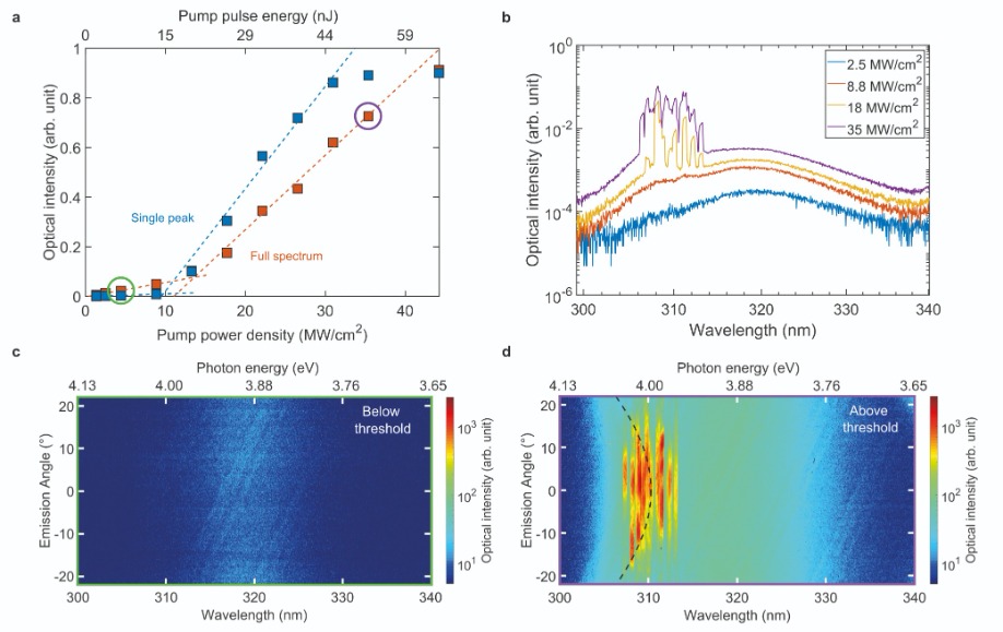
Figure 6. Optically pumped UVB VCSEL characteristics. (a) Optical output intensity at room temperature, integrated around a single lasing peak and over the entire emission spectrum, as a function of pump power density and energy per pulse. (b) Optical emission spectra at different pump power densities. (c) Angle-resolved spectra in a logarithmic scale below threshold and (d) above threshold. The green and purple circles in (a) mark the data points corresponding to (c) and (d) and the black dashed line in (d) marks the simulated longitudinal cavity mode. The spectral resolution was 0.5 nm.
Note that great care is required when trying to compare these threshold pump power densities with those published for blue or UVA VCSELs, or for optically pumped UV edge-emitting lasers. Complications arise from the shorter carrier lifetimes of UVB material, and difficulties in estimating the reflectivity of the pump beam from the sideband of the DBR, where reflectivity strongly varies with wavelength.
Increasing the pump power drives a shift in the output of our UVB VCSEL from a spectrally broad spontaneous emission to, above threshold, several high intensity peaks each with a narrow width – that is, less than 0.15 nm (see Figure 6(b)). Angular-resolved photoluminescence below threshold shows that there is emission in all angles and it is non-dispersive, as expected from spontaneous emission (see Figure 6 (c)). Above threshold, there is a transition to a well-defined beam with non-dispersive laser lines, a strong indication of lasing (see Figure 6(d)).
New adventures
For any emerging class of laser, the first important milestone is the demonstration of lasing under optical pumping. With this now accomplished, our next target is to make a useful VCSEL out of this optically pumped device. This goal, implying electrical operation, is far from trivial. It requires improvements in many different areas, to minimize losses and maximize modal gain, with efforts needing to include: an improvement in surface morphology, through optimisation of both the epitaxial growth and the electrochemical etch process; a reduction in defect densities; better heat removal; and the introduction of optical guiding structures. Such efforts will also reduce the filamentation that occurs in our latest devices.
Crucial to our success is the development of an electrical injection scheme. We believe that the most promising way forward is to introduce tunnel junctions, with an n-doped AlGaN-layer on top of the tunnel junction providing transverse current spreading. Recent work by other groups have highlighted the promise of the AlGaN-based tunnel junctions, but if it is to flourish in a VCSEL instead of in an LED, this junction will need to operate at a far higher current density – in the region of tens of kiloamps per square centimetre – and have a very smooth surface, to ensure low optical loss.
Time will tell whether efforts on UV VCSELs amount to just curiosity-driven research that attempts to push technology to its limits, or are a development that has a strong impact on society. Our view is that our technology will play a key role in helping to propel the VCSEL to the UVC, where it could be used to combat the spread of bacteria and viruses. We want to make these lasers as useful as their infrared-emitting cousins, providing an invisible source of light in our daily lives.
Our AlGaN-membrane technology, critical to our fabrication of the cavity, has uses beyond just UV VCSELs. We have already demonstrated that it can aid thin-film flip-chip UV LEDs. In future, it may also assist efforts to create high-quality waveguides for non-linear applications, help transfer high-power HEMTs to any desirable heat sink, realise high-quality microdisc lasers, and enable the reuse of precious GaN and AlN substrates.
In this context it is interesting to mention the German physicist, chemist and philosopher Johann Wilhelm Ritter. A pioneer of electrochemistry in the early 1800s, Ritter also proved the existence of ultraviolet light. Now, some 200 years on, it is rather fitting that we have benefitted from his research by using electrochemistry to create a UV light source. As little as he could predict that this would be one of the outcomes of his research, it is hard for us to foretell the usefulness of our AlGaN-membrane technology and short-wavelength UV VCSELs. We will leave it up to the research community to explore and demonstrate.
When grown on GaN, AlPN creates a strong polarization that promises to enhance the performance of the high-frequency HEMT
BY MARKUS PROSTOVEK FROM NAGOYA UNIVERSITY
MOST OF US have never encountered a new material. While it’s certainly not unusual to change from one material system to another during a career – migrating from classical III-Vs to the III-nitrides is a well-trodden pathway – it is rare to be there first. Even in academia, which fosters a more adventurous outlook than industry, incremental improvements are the norm, with research tending to be driven by opportunities identified within new applications.
This state of affairs is particular true in the III-Nitrides. In addition to AlN and GaN, just three ternaries are used for all devices – AlGaN, InGaN, and AlInN – with the latter of these rarely employed. Using ternaries brings challenges, primarily strain, with only Al0.83In0.17N offering lattice-matching to GaN. In sharp contrast, it is relatively easy to realise lattice matching with the more traditional III-Vs. Best known is the pairing of GaAs and AlGaAs, which unite to make the highly reflective mirrors of a VCSEL; but don’t forget the great versatility of InGaAsP, which offers compositions that can be lattice-matched to GaAs or InP while realising bandgap engineering.
Several attempts have been made to broaden the III-nitrides material portfolio. A pre-requisite for any such effort is a suitable metal-organic precursor, since all commercial growth uses MOCVD.
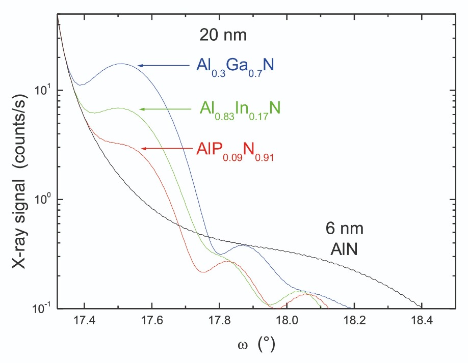
Figure 1. Calculated X-ray diffraction around (0002) GaN for HEMT structures on GaN with different materials, assuming 106 counts/s for GaN (0002).
More recently, attempts have been made to alloy scandium to form AlScN-on-GaN, a promising combination for realizing high polarization in an RF HEMT. Using MBE, researchers have grown layers of wurtzite AlScN that are stable for a scandium content up to 50 percent. Replicating these results in MOCVD has been very challenging, because metal-organic scandium-based precursors have a very low vapour pressure. There are also concerns over purity, although it is improving.
Arsenides and phosphides
If the starting point to develop a new material is a proven metal-organic precursor, then deciding to incorporate either arsenic or phosphorous is a logical way forward. After all, both are used a lot in classical III-Vs.
Some effort has already been devoted to alloying arsenic into GaN. The problem is that as arsenic is an even larger atom than gallium, it cannot squeeze into the tiny space of a nitrogen-lattice site. Due to this, in wurtzite GaAsN almost more arsenic goes on a gallium lattice site than there is on an nitrogen lattice site. Another impediment to the growth of GaAsN is that there is a low bond energy for an arsenic atom on a nitrogen site, causing arsenic to mostly desorb at the high growth temperatures required for epitaxy.
This leaves phosphorous. With a covalent radius between gallium or aluminium and nitrogen, it should be a little easier to incorporate phosphorous than arsenic on a nitrogen-lattice site.
Between 1996 and 2006, researchers tried to develop the growth of wurzite GaPyN1-y on GaN. This effort delivered limited success, realising homogenous layers with a phosphorous-content up to 3 percent. However, when attempts were made to produce films more rich in phosphorous, this lead to the formation of two classes of imperfection: phosphorous-antisites, that is phosphorous atoms located where gallium atoms should be; and PxNx clusters, attributed to both the shorter bond length of P-N than Ga-N and the larger size of phosphorous than nitrogen. These defects are driven by strain: when GaPN is grown on GaN this ternary is compressively strained, so the presence of phosphor on a gallium site can reduce this strain. This inherent limitation put an end to research on GaPN.
What about AlPN on GaN? This has much promise: AlN is tensile strained on GaN, so beyond the valences, phosphorous atoms have a further incentive to stay on the group V site. Note that this is not a new idea. Back in 1999 a team at Panasonic filed a patent associated with the strain relaxation potential, proposing AlGaNP instead of AlGaN. However, no experimental results were ever published.
Since 2012 I have been keen to investigate the prospects of AlPN on GaN. I didn’t get the chance to pursue this when working as a postdoc, but when I took up the position of a Designated Professor at Nagoya University in 2017 the situation changed and I finally got to the chance to try and grow this new ternary, using a closed coupled showerhead reactor made by EpiQuest.
One obvious candidate for the source of phosphorous is PH3. For us, however, phosphine is not an option, due to its toxicity that prevents its use in our lab – but that’s not a disaster, as even if our team had been granted permission, it’s not trivial for us to use this source, as it would demand new bottle cabinets, security electronics and scrubbing systems. Instead we’ve turned to the liquid precursor tertiary butylphosphine (tBP). This is a move that has taken me full circle, as I helped to evaluate this less toxic phosphor precursor during my diploma thesis. (In the run up to the turn of the century tBP was developed to a high standard, when California thought about banning the use of PH3.) We started by hooking up the tBP bubbler to a repurposed MO line.
Getting going
Uncovering suitable growth conditions is the first task when trying to grow any new material. Luckily, for AlPN we did not have to start from scratch, as we could draw on what’s been accomplished for AlN, which is closer to AlP than you may think.
These efforts have been aided by access to a handful of reports on the growth of cubic AlP, as well as my own attempts at trying to grow this material ten years ago. All those efforts involved cranking up the temperature of the reactor to its maximum – so between 750 °C and 950 °C – and employing relatively low V/III ratios, in the range 20-100. These conditions are similar to those for AlN growth, which again uses as high a temperature as possible – in this case between 1150 °C and 1250 °C – and V/III ratios of 50-100.
For our starting point we chose 1100 °C, a half-way house that still allows the growth of good GaN. We also selected a low V/III ratio. This is not only an obvious choice, based on the conditions used for the growth of AlP and AlN, but helps to reduce the impact of contamination and trim development costs, because tBP is relatively expensive compared with NH3 and PH3.
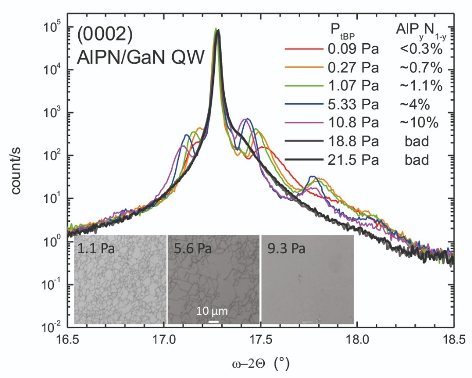
Figure 2. X-ray diffraction from multiple AlPN/GaN quantum wells with increasing tBP partial pressure grown at 1100°C.
Given these difficulties, it’s of no surprise that the X-ray diffraction spectra for our first superlattices showed relatively broad peaks and an absence of clear Pendellösung. Still, we were able to use the zero-order peaks to calculate the phosphorous content. For this, we had the good fortune of being able to draw on the calculation of lattice constants and elastic constants for wurtzite AlP (and many other materials), undertaken in The Materials Project. When carrying out our X-ray calculations, we used corrected versions of calculated lattice constants, adjusted using the same factor needed to match the calculated lattice constants of AlN to their experimental values.
Assuming a similar growth rate to that of GaN for thick layers, we estimated X-ray spectra for AlPN-based superlattices with a phosphorous content up to 10 percent. When the phosphorous content exceeded this figure, we found that the features in the X-ray spectra associated with the quantum wells completely vanished, to leave just a broad shoulder (see Figure 2).
This observation is consistent with our hypothesis that tensile strain is critical: at a concentration of 11 percent the AlPN layer becomes compressively strained, with excess phosphorous forming black adsorbing PxNx clusters. It’s the same state of affairs when an AlPN layer cracks. The relaxed (cracked) AlPN has less than 3 percent AlPN, with excess phosphorous forming inclusions. It is clear that the key to growing AlPN with a higher phosphorous content is to avoid compressive strain or relaxation.
The good news is that when it comes to fabricating a HEMT, a thin layer suffices. For high-frequency HEMTs, what matters most is as high a polarization as possible. Currently AlInN provides this, while AlScN, under research, could yield far higher polarization charges (see Figure 3). However, growing AlScN by MOCVD is very challenging. AlPN has much promise, with a composition of AlP0.05N0.95 offering a similar degree of polarization to AlScN. Thanks to strong impact on the lattice constants of even a low phosphorous content, the critical thickness for this ternary is in excess of 20 nm.
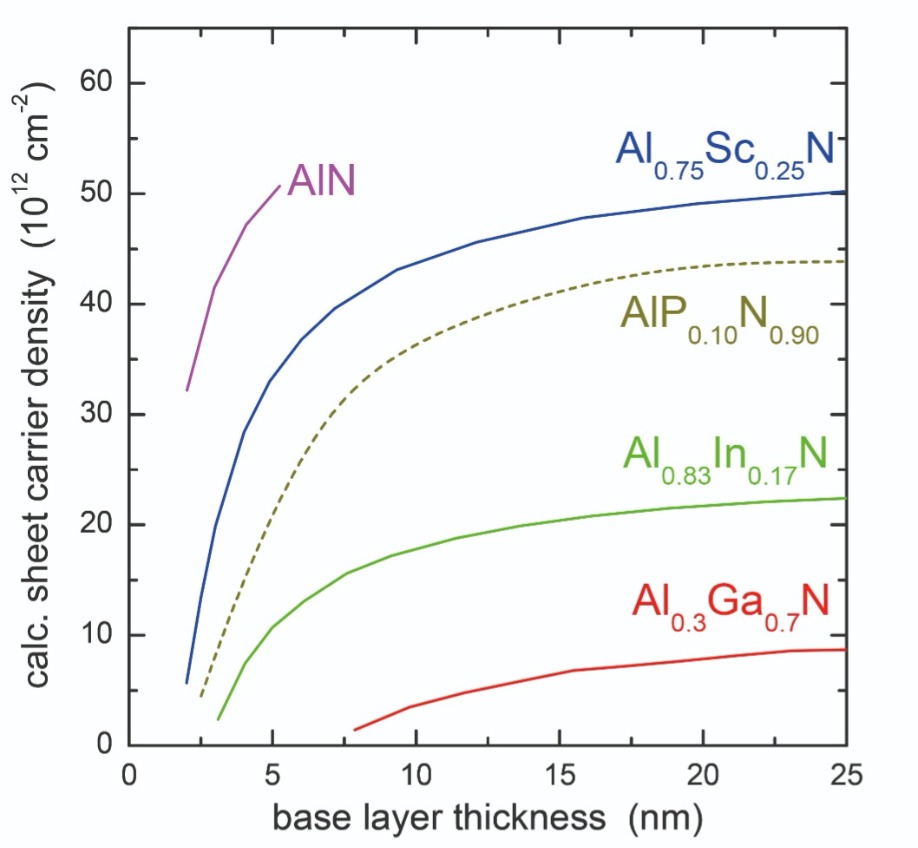
Figure 3. Calculated sheet carrier density in HEMT structures using different barrier materials. Adapted from T. Kazior et al. 2019 IEEE/MTT-S International Microwave Symposium. The curve for AlPN has been added assuming that the polarisation coefficients of AlP0.1N0.9 are similar to Al0.9Ga0.1N.
An open question is the optical properties of AlPN. To ensure high-quality, this layer must be thin. We have found that when the thickness is below 60 nm, carriers drift into the neighbouring smaller bandgap GaN layers, where recombination takes place. So the unambigeous confirmation of the band gap bowing is still in the long homework list for this material.
Reactor modifications
Our success has been hard won, and there are still many challenges to overcome that are associated with the growth of AlPN. To cater for the much higher vapour pressure of group V atoms, much higher partial pressures are needed for the group III sources compared with traditional values for the growth of aluminium-based materials. These higher pressures can lead to surface reactions, where one component partly replaces another on a surface even without growth. The solution to combatting these issues is to introduce a proper switching sequence when going from GaN to AlPN. This approach is commonplace in the classical III-Vs, employed for instance when growing InGaP on GaAs – this requires switching sequences with a pre-flow of one of the group V gases. We have adopted a similar approach after barrier growth at the AlPN/GaN interface. In our case, we have found that when going from GaN to AlPN, a tBP preflow between 5 s and 20 s improves X-ray reflection. We still need to study the interface formed by growing GaN on AlPN.
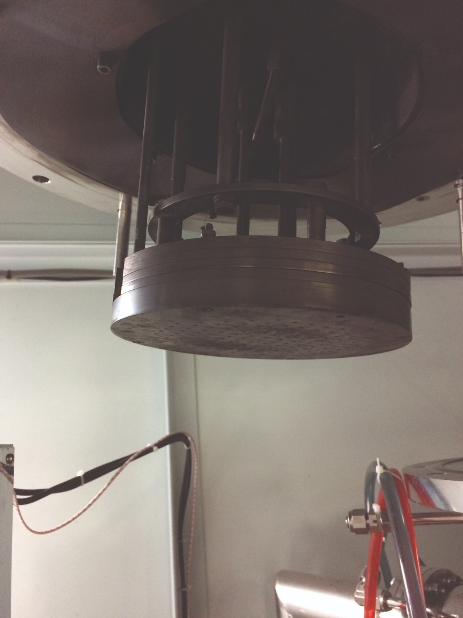
As well as surface reactions, we have had to account for vapour phase reactions between the aluminium precursor (trimethylaluminium, TMAl) and tBP, which pose similar consideration to TMAl and NH3. Until recently, we would introduce tBP via an empty MO-line. With that configuration, after passing the run/vent valves, TMAl and tBP precursors would travel together
for 1.5 m before entering the showerhead together. It was not an ideal set-up, leading to strong particle formation and a strong carry over of phosphorous into the subsequent runs, probably due to deposition inside the lines and showerhead. We successfully addressed this issue this January by changing the tBP inlet to the group V manifold. Unfortunately, this modification has impacted the relationship between tBP flow and phosphor incorporation, so we need to revise our growth conditions.
There is no doubt that AlPN has much promise. Success is not easy, with growth still the main challenge, but we have begun work on our HEMTs.
Multiple channels and innovative edge termination enable GaN Schottky power rectifiers to combine low epitaxial costs with operation up to 5 kV
BY YUHAO ZHANG AND MING XIAO FROM VIRGINIA TECH AND HAN WANG FROM THE UNIVERSITY OF SOUTHERN CALIFORNIA
RECTIFIERS providing high switching speeds and withstanding up to several kilovolts are in much demand. They are needed in power electronics systems used in the electricity grid, renewable energy processing, and industrial motors (see Figure 1).
Today, the most widely used device for rectification is the bipolar silicon p-n junction diode, despite its major drawback – a very slow switching speed, stemming from poor reverse recovery. A superior alternative that allows fast switching is the SiC Schottky barrier diode (SBD). However, its performance has only recently caught up with that of the silicon p-n diodes, and its epitaxial and fabrication costs are far higher.
Another material offering even more promise for high-voltage rectifiers is GaN: compared to silicon and SiC, it has the upper hand in several key areas, having a wider bandgap, higher mobility, and a higher critical electric field. Drawing on these strengths, several companies have launched GaN power devices with a lateral geometry, operating at up to 650 V. This geometry is challenging, limiting current and power capabilities, because current conduction takes place in a layer just a few nanometres thick – that’s a consequence of the two-dimensional-electron gas (2DEG) channel. Note that this impairment does not arise in high-voltage silicon and SiC devices, because they usually have a vertical architecture, with current spreading into bulk materials.
One major drawback, resulting from the limited current capability of GaN power devices with a lateral geometry, is the need for larger die sizes when accommodating high voltages and high currents. As well as increasing chip costs, the larger die induce large capacitances and charges, compromising device switching speed.
To overcome these challenges, our team at Virginia Polytechnic Institute and State University (Virginia Tech), working in collaboration with engineers at Enkris Semiconductor, Qorvo and the University of Southern California, has developed a novel high-voltage lateral GaN technology that features multiple channel materials and innovative anode structures.
We fabricate our devices from 4-inch AlGaN/GaN-on-sapphire wafers that host five stacked 2DEG channels and are produced by Enkris. A five-fold increase in the number of 2DEG channels compared with a conventional structure increases current capability by at least that factor, and delivers a corresponding reduction in sheet resistance. Around the multi-channel fins is wrapped a new anode architecture, comprising p-n junctions. This structure shields the Schottky contact from a high electric field and suppresses the leakage current for the five-channel device to below that for a single-channel counterpart. The performance of the novel multi-channel GaN Schottky rectifier is impressive, boasting a power figure-of-merit that exceeds the unipolar SiC limit, and is among the highest in all high-voltage rectifiers.
Stacking 2DEG channels
When engineers design power devices, efforts centre on the concurrent realization of a high breakdown voltage and a low on-resistance – for a lateral GaN rectifier, the latter is the product of sheet resistance and anode-to-cathode distance. While this distance is usually determined by the breakdown voltage, the on-resistance hinges on the sheet resistance, which can be trimmed by increasing the mobility and density of the 2DEG. As the number of channels increases through stacking, the density of the 2DEG increases proportionally. In turn, die size for a specific current rating can be greatly reduced, leading to smaller capacitance and charges, and ultimately a higher switching speed and lower losses.
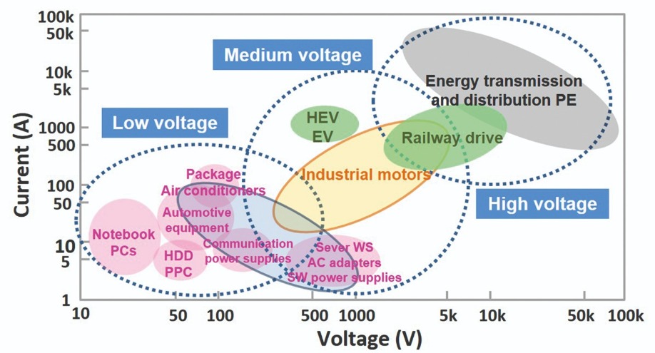
Figure 1. Application space of power rectifiers with different voltage and current ratings.
Very recently, the most common approach for the production of compound semiconductor devices, MOCVD, has been used to manufacture multi-channel structures on a variety of large-diameter substrates, including silicon, SiC, sapphire, and GaN. It is this growth technology that Enkris has employed to produce 4-inch, five-channel, GaN-on-sapphire wafers that feature a 2DEG with a density of 3.7×1013 cm-2 and a mobility of 1475 cm2 V-1 s-1. The corresponding sheet resistance is just 110 Ω/sq, a figure at least two times lower than the best value for a single-channel wafer. We estimate that the cost of this multi-channel GaN-on-sapphire wafer is no more than a third of that of a 4-inch SiC wafer.
Cranking up the voltage
Scaling up the voltage of multi-channel devices is much more challenging than it is for their single-channel counterparts because the increased charges from multiple channels threaten to induce electric-field crowding. However, overcoming this challenge is crucial for Schottky rectifiers, because their blocking voltage tends to be limited by the peak electric field at the Schottky contact region.
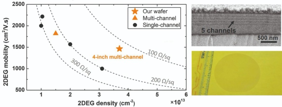
Figure 2 (left) 2DEG density versus 2DEG mobility for the single-channel and multi-channel AlGaN/GaN materials reported in the literature and measured on the wafer detailed in this article. (right) cross-sectional scanning electron microscopy image and top-view photo of the 4-inch, five-channel, GaN-on-sapphire wafer produced by Enkris Semiconductor Inc.

Figure 3. A conventional field plate termination (left) and Virginia Tech’s novel p-GaN termination (right). Two channels are drawn to illustrate multi-channel structures.
Minimising device leakage
When developing our high-voltage multi-channel devices, the challenges we faced included minimising leakage current. Our solution is the junction-fin-anode. This is a three-dimensional anode structure, formed by wrapping p-n junctions around the multi-2DEG-fins (see Figure 4(a)). With this architecture, the p-type material provides strong depletion of the 2DEG channels. When the device is reverse biased, the junction-fin assists the Schottky contact for charge depletion, while shielding the Schottky contact from a high bias.
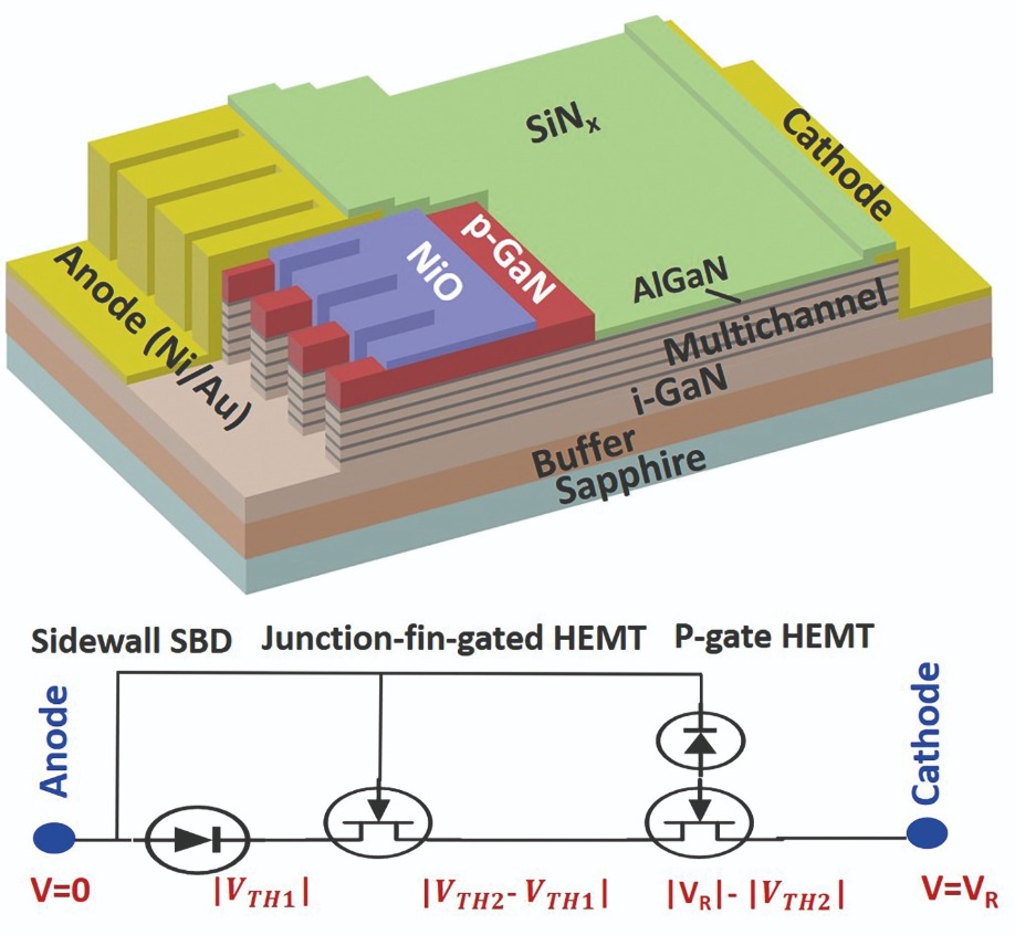
Figure 4 (top) Virginia Tech’s multi-channel Schottky rectifier with a junction-fin anode. (bottom) Equivalent circuit model of the rectifier, comprising a series combination of a sidewall Schottky barrier diode, a junction-fin-gated HEMT, and a p-gate HEMT. The internal voltage distribution under a high reverse bias (VR) is also illustrated, with the threshold voltages of the junction-fin-gated HEMT and p-gate HEMT marked as VTH1 and VTH2, respectively. The voltage drop on the sidewall Schottky barrier diode is clamped at | VTH1| regardless of VR.
In our prototyped device, we realise the junction-fin structure by regrowth of p-GaN on top of the fin, and the addition of a p-type nickel oxide at the fin sidewalls. The resulting rectifier delivers a blocking voltage up to 5.2 kV, and when operating at 90 percent of this limit, the leakage current is just 1.4 μA/mm. The specific on-resistance is 13.5 mΩ cm2. Based on all these values, we find that the power figure-of-merit for our device exceeds the SiC unipolar limit and is among the highest in all multi-kilovolt power SBDs.
We have also fabricated large-area devices. They are capable of handling a 1.5 A current, have a leakage current measured in microamps, and a total charge of 13 nC (see Figure 5). Compared with commercial SiC SBDs with similar voltage and current ratings, our multi-channel GaN SBDs exhibit a significantly lower forward voltage and charges.
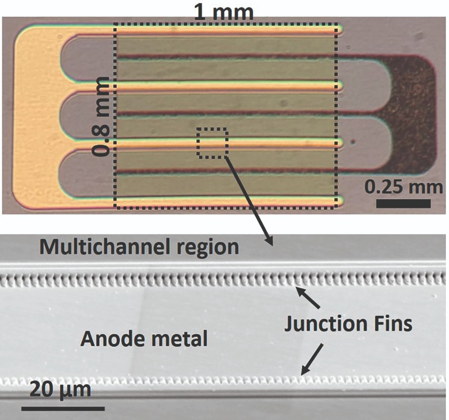
Figure 5 Top-view microscopic images of the fabricated 1.5 A, 5 kV GaN power Schottky rectifier.
M. Xiao et al. “5 kV Multi-Channel AlGaN/GaN Power Schottky Barrier Diodes with Junction-Fin-Anode”, 2020 IEEE IEDM, 5.4.
M. Xiao et al. IEEE Electron Dev. Lett. 41 1177 (2020)
Y. Ma et al. Appl. Phys. Lett. 117 143506 (2020)
According to Precedence Research in a report from January 8, 2021, the global electric vehicle (EV)market is expected to grow by more than 40 percent by 2027. What it says, among other things, is that the supply chain for chips and modules powering these vehicles needs to evolve immediately. One of the obvious shifts will be moving away from traditional devices made from silicon and toward devices made from compound semiconductor materials such as SiC. At higher voltages needed for EVs, the performance properties of SiC far outpace those of silicon, but the supply chain for SiC is not nearly as mature.
The global EV market needs SiC to catch up…and quickly.
Integrated Device Manufacturers (IDMs), already well-versed in silicon, needed a pathway to produce SiC devices and modules for rapidly accelerating EV demand. But SiC is more complex because it comes from a crystal that is extremely difficult to grow, and that presented a bottleneck.
It is against this backdrop that GTAT (www.gtat.com) began forging a business model in 2017 to become a ‘pure-play’ producer of wafering-ready SiC. The company’s focus on growing SiC bulk crystal and staying away from wafering and device-making is an important distinction. “We have a core competency, and that’s crystal growth,” says GTAT President and CEO Greg Knight. “There are tremendously talented companies around the world that know how to make wafers and devices, but what they don’t necessarily have is a way to grow the SiC crystal. They need the material, and lots of it.”
GTAT’s heritage as a producer of crystal growth equipment means that it can ‘scale up’ capacity very rapidly. The knowhow needed to design and build crystal-growth furnaces is the essence of GTAT’s DNA. “We are able to bring SiC capacity to market faster than anyone,” said Knight. Indeed, the company has hit milestones extraordinarily rapidly. “We made our CrystX silicon carbide n-type material available to customers in 2018, less than a year after opening our facility,” said Knight. A year after that GTAT achieved ISO 9001:2015 certification and signed the first of several long-term supply agreements with key customers for 150 mm diameter boules.
Fundamentally, SiC is not a defect-free material and is challenging to make at the high quality levels customers demand. That is why most of the companies invested in making SiC wafers and devices do not have the experience to also make the crystal material itself. The equipment used to make silicon cannot be used for SiC, and the capex (and time) required to develop in-house SiC growth is significant. “We understood this early-on,” said Knight. “We knew that SiC was going to become the base material for semiconductors used in growing applications such as EV.”
The fact that SiC is not defect-free means that GTAT has spent considerable resources to drive those defect rates down. The chart (left) shows GTAT’s very aggressive trend since introducing its CrystX silicon carbide material.
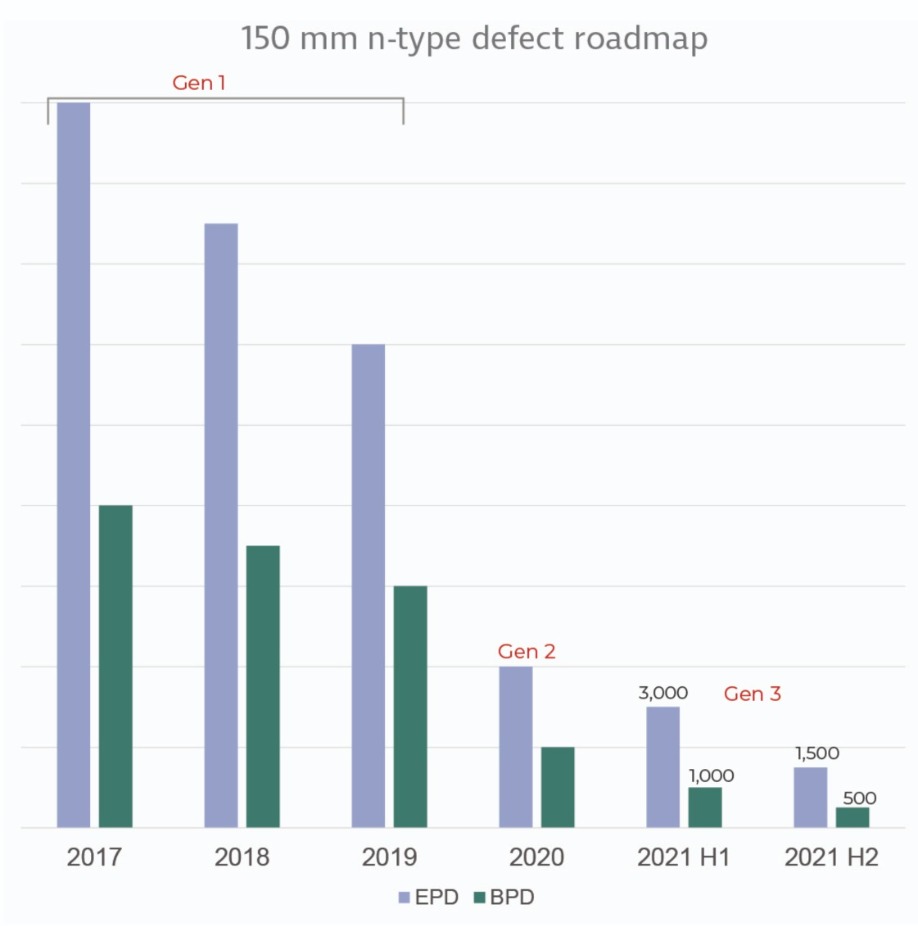
GTAT is driving defect rates down significantly and rapidly
Specifically, Etch Pit Density (EPD) and Basal Plane Dislocations (BPD) are critical quality metrics for SiC. GTAT has made significant progress driving down BPD’s to less than 1,000 per cm2 and is set to reduce this by another 50 percent in the near term. Much of GTAT’s focus has been on reducing defects through continuous improvement. “This is what our customers demand, and we deliver,” said Knight. “We have a longstanding heritage in building the equipment we now use ourselves, and we couple that with a high level of process excellence.” GTAT’s inherently stable production process enables all its high-quality material to be made to this standard, which is available under a single product grade.
While continuous improvement is a function of GTAT’s increased cycles of learning and optimization, R&D efforts allow the company to push forward on 200 mm diameter SiC as well as semi-insulating (SI) SiC for RF applications. Both product launches are expected in late 2021 or early 2022. To support existing 150 mm demand while forging ahead with 200 mm and SI, GTAT is currently growing production capacity by 60 percent on top of what exists today. With multiple supply agreements in place, the ability to ramp up quickly puts GTAT in a perfect position. “Rapidly growing markets like EV require a very nimble supply chain, and we’re able to respond,” said Knight. This round of expansion will be completed by early Q3 2021, with more expected as partners continue to scale their demand.
The increased R&D capacity will be used to further the company’s efforts on SI CrystX SiC and its transition to larger 200 mm boules. As 5G continues to roll out globally, the need for semi-insulating SiC will accelerate. There are many RF-related applications for SI SiC, and GTAT’s R&D efforts are focused on bringing this to market quickly. In addition, the transition from 150 mm to 200 mm diameter SiC is necessary to boost yields. The 78 percent increase in wafer surface area means a corresponding increase in the number of devices, which helps lower cost. “Higher quality and bigger-diameter boules are parallel efforts for us,” said Knight. “We are moving very rapidly in response to a very dynamic and fast-growing set of markets.”
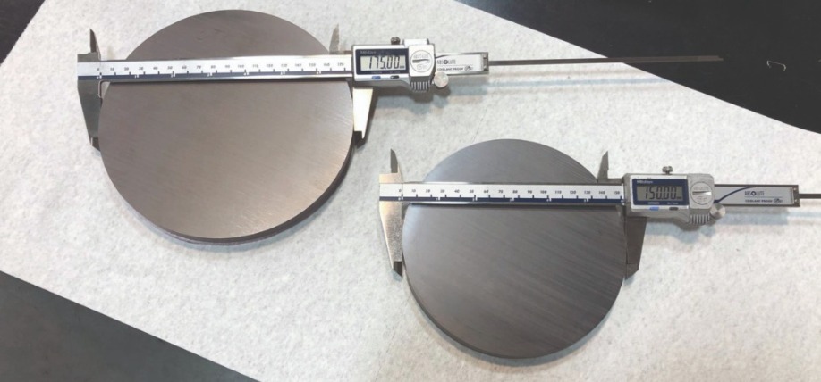
Introduction of 200mm diameter. SiC will occur later in 2021
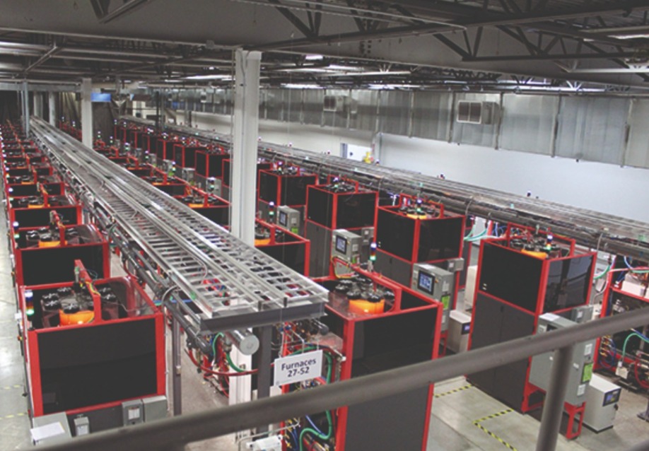
GTAT will be expanding its production capacity by 60 percent in 2021.

GT Advanced Technologies is a manufacturer of high-performance crystal materials including silicon carbide (SiC) and sapphire. GTAT’s corporate headquarters in Hudson, New Hampshire also serves as the Company’s primary manufacturing facility for its CrystX silicon carbide. This material is fundamental to the production of semiconductors used in electric vehicles and other power electronics applications.
Directly contact:
Christopher Van Veen
chris.vanveen@gtat.com for more information, or visit us at: https://gtat.com/products/silicon-carbide

Nichia raises the bar for blue and green VCSEL efficiency
VCSELs with dielectric and GaN-based mirrors break efficiency records
Nichia is claiming to have broken the efficiency records for GaN-based blue and green VCSELs.
These triumphs, announced at the SPIE Photonics West meeting this March, return this Japanese LED and laser diode manufacturer to the forefront of GaN-based VCSEL development. Nichia pioneered this class of laser more than a decade ago, producing the world’s first GaN-based VCSEL operating in continuous-wave mode at room-temperature, before appearing to abandon further development for many years.
Speaking on behalf of the company at Photonics West, Kenichi Terao revealed that the primary target for these VCSELs is the light source in smart glasses. In these retinal displays, red, green and blue sources only need to produce a milliwatt a most – a specification met by the team’s latest lasers.
Nichia’s first foray into VCSEL development brought much initial success. Milestones from that era included a violet-emitting room-temperature VCSEL operating in CW mode in 2008, and blue and green siblings in 2011 and 2012. However, the fabrication process for this design, featuring a pair of dielectric mirrors, is incompatible with mass production. To define the dimensions of the cavity, epilayers must be removed from the substrate and polished down to the ideal thickness. Unfortunately, this cannot be accomplished routinely at the nanometre scale, preventing mass production with acceptable yield.
To overcome this issue, Terao and co-workers have turned to a design that combines a dielectric top mirror with a bottom mirror based on an Al0.8In0.2N/GaN distributed Bragg reflector. Although this team are not the pioneers of this architecture, they have made significant advances with it, including the first lasing in the green, and record-breaking efficiencies for all forms of GaN-based VCSEL.
The team’s blue VCSELs have: a dielectric DBR made from the pairing of SiO2 and Nb2O5; a 4 μm-diameter aperture defined by passivation of the p-GaN surface; and a cavity length equating to just 4.5 l, ensuring that this design is short enough for single-mode lasing.
These devices emit at 442.3 nm, have a threshold current and voltage of 0.40 mA and 3.75 V, and produce a peak wall-plug efficiency of 13.6 percent. Measurements on seven of them, each producing 0.6 mW when running at 25 °C, reveal stable CW operation beyond 1,000 hours.
Formed from epiwafers featuring a 2-inch GaN substrate, yield for these blue VCSELs exceeded 90 percent. This figure considered an exclusion zone of less than 4 mm, included to exclude material very close to the edge of the wafer, where photolithography processes are unstable.
Driving currents of 1 mA, 3 mA and 5 mA produced a single peak for the VCSELs, indicating a stable single longitudinal and single transverse mode. Emission wavelength shifted by 0.11 nm /mA, due to changes in refractive index resulting from self-heating. Further investigations of self-heating uncovered a variation of 0.017 nm/°C, which is smaller than that for an edge-emitting laser, according to Terao.
The design of the team’s green VCSEL is very similar to its blue cousin. Terao said that the primary difference is a larger aperture – it’s been widened from 4 μm to 5 μm – to prevent an increase in drive voltage. The green VCSEL also features a thinner active layer, to supress the piezoelectric field.
Characteristics of the green VCSEL, which emits at 514.9 nm, include a wall-plug efficiency of 3.7 percent, a threshold voltage of 5.02 V and a threshold current of 2.8 mA. Optical output power is over 1.5 mW, smashing the previous record of 0.1 mW held by Sony.

Nichia will target smart glasses with its GaN VCSELs
K. Terao et al. SPIE Photonics West 11686-1 (2021)

Enhancing AlN-on-sapphire templates with thermal cycling
Repeated thermal cycling slashes the threading dislocation density in sputtered AlN films grown on sapphire
Researchers at Mie University, Japan, have improved the quality of AlN-on-sapphire templates by thermal cycle annealing.
Their process, which drives down the dislocation density in AlN films, should help to increase the prospects for the deep-UV LED. Fabricating this device on a low-cost, high-quality substrate promises to increase its output power and drive its deployment in various applications, including medical treatment, water purification, and solar-blind communication.
Interest in AlN-on-sapphire templates has been fuelled by a lack of progress in bulk AlN, which is pricey and limited in availability and size. Turning to AlN-on-sapphire templates addresses all these issues, but the deposited layer can be riddled with defects, resulting from the large lattice mismatch with the substrate. Thicker layers can trim the threading dislocation density, but at the expense of wafer bow that leads to processing issues.
Back in 2016, the team from Mie University reported that they could reduce the threading dislocation density by one-to-two orders of magnitude with a process that included producing a pair of AlN-on-sapphire substrates by sputtering, and then placing the growth surfaces face-to-face and annealing under nitrogen gas. Building on this work, the team have managed to further reduce the dislocation density by double sputtering and annealing. This quashes the threading dislocation density to below 108 cm-2, but the process is not trivial, requiring two sputtering and annealing steps, with success hinging on keeping the surface clean prior to the second sputtering.
To simplify the process, the team recently investigated thermal cycle annealing, evaluating the impact of different cycles on a range of AlN films with thicknesses varying from 100 nm to 1000 nm. A range of thermal cycling conditions included variations in the number of ramps, the magnitude of the temperature difference, and whether with a two-step anneal it is better to use a higher temperature at the beginning or the end.
The team also investigated the impact of extending the time for annealing, considering a 370 nm-thick AlN film at a constant temperature. As time increased from 1 hour to 12 hours, the threading dislocation density fell from nearly 5 x 108 cm-2 to less than half this value. However, the longer times introduced other issues: macroscopic defects started to appear after 9 hours, due to the formation of AlON; and the interface between AlN and sapphire started to deteriorate, becoming unsuitable for growth.
For the range of thermal annealing conditions applied, the best results came from a five-cycle ramp between temperatures of 1600 °C and 1700 °C. With this approach, involving holding the sample for 72 minutes after each temperature change, the threading dislocation density fell to 1.65 x 108 cm-2.
According to the team, when the AlN film is simply annealed at 1700 °C, the weak tensile strain relaxes, to leave almost no strain. By alternating temperatures between 1600 °C and 1700 °C, this allowed the lower temperature to induce compressive stress, which accelerates the movement of dislocations and ultimately increases the likelihood of annihilation and coalescence.Using these conditions, but increasing the AlN film thickness to 800 nm, resulted in a further decrease in threading dislocation density to 8 x 107 cm-2.
The team has produced deep-UV LEDs on this high-quality template, and for comparison, on a variant formed by MOCVD. Compared to the control, the multi-quantum wells in the low threading dislocation density templates had a dark spot density that is lower by almost an order of magnitude. Output power for the device with the high-quality template is 80 percent higher. Further improvement in this figure is anticipated by optimising growth conditions, the substrate off-cut angle, and the hole injection layer.
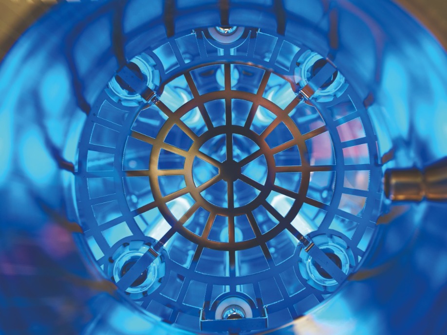
High-quality AlN-on-sapphire templates will help deep-UV LEDs replace lamps for water purification
D. Wang et al. Appl. Phys. Express 14 035505 (2021)

Mist-CVD enhances MIS-HEMTs
Thanks to mist CVD, pyrophoric materials and vacuum pumps are no longer needed to deposit insulators on GaN HEMTs
A Japanese collaboration is claiming to have produced the first metal-insulator-semiconductor (MIS) HEMTs with an alumina insulator added by mist-CVD, a cost-effective, environmentally friendly growth process.
This variant of the HEMT is less common than that with a Schottky gate, which has a simpler architecture, is easier to make, and produces a high transconductance. However, the Schottky gate HEMT does have a drawback: it suffers from high leakage currents, originating from high input swings that drive the gate to forward bias. Addressing this issue is the MIS structure, formed by inserting an insulator between the AlGaN layer and the metal gate.
Unfortunately, the established deposition techniques for realising the MIS-HEMT requires the use of highly flammable toxic sources under vacuum. For example, the common approach to adding alumina (Al2O3) – an insulator with a high breakdown field and good permittivity – is atomic layer deposition, using trimethylaluminium, a highly pyrophoric material.
In comparison, the mist CVD technique pursued by the Japanese team – a partnership between researchers at the University of Fukui, Kwansei Gakuin University and Kumamoto University – is cost-effective and environmentally friendly, with deposition taking place at atmospheric pressure, so there is no need for energy-hungry vacuum pumps.
“On top of that, the mist CVD system employs far safer and cheaper aluminium acetylacetonate as the aluminium source,” says team spokesman Joel Asubar from the University of Fukui.
Asubar champions the simplicity of the technique, pointing out that a mist CVD system has just two major parts: an atomiser, which is very similar to a commercial ultrasonic humidifier; and a heater. The challenge is to control the flow of the mist, which is part liquid, part gas. According to Asubar, it is knowledge of hydrodynamics and the pyrolysis reaction of the source precursor that has unlocked the “secret recipes” for depositing alumina over a semiconductor surface.
To demonstrate the capabilities of mist growth, the team compared the performance of devices produced by this approach with those incorporating a Schottky gate. Both types of transistor were fabricated from epiwafers featuring a SiC substrate and a 24 nm-thick AlGaN barrier – this ternary created a two-dimensional electron gas with a sheet carrier density of 1 x 1013 cm-2 and a mobility of 1510 cm2 V-1 s-1.
Fabrication of the HEMTs began by reactive-ion etching, which defined isolation trenches, and electron-beam evaporation that provided source and drain contacts. To make the MIS-HEMT, the team added Al2O3, using a mist created by dissolving aluminium acetylacetonate in methanol and atomising this liquid precursor with a 2.4 MHz ultrasonic transducer. Using a nitrogen carrier gas, it took just 90 s to deposit this film on a sample heated to 400 °C.
Merits of the MIS-HEMT made by mist CVD over that with a Schottky-gate have been demonstrated by measurements on devices with a 3 μm long, 100 μm wide gate and gate-to-drain and gate-to-source spacings of 10 μm and 4 μm, respectively. Gate leakage current is three orders of magnitude lower, allowing the application of a +3V gate-source that boosts the maximum drain current to 780 mA mm-1. In addition, the reverse breakdown voltage is higher – it is 320 V, compared with 210 V.
Asubra has also compared his MIS-HEMT with those made by ALD that employ the same insulator. Those made by mist-CVD have an interface state density that tends to be lower and a sub-threshold swing that is said to be “highly competitive”.
One of the collaboration’s next goals is to build on recent work that uncovered an unexpectedly low level of fixed positive charges at mist-Al2O3/AlGaN interfaces. “This means that it would be easier to obtain enhancement-mode devices using mist-Al2O3,” says Asubar, who intends to use this feature to obtain high-performance, safer ‘normally-off’ devices.
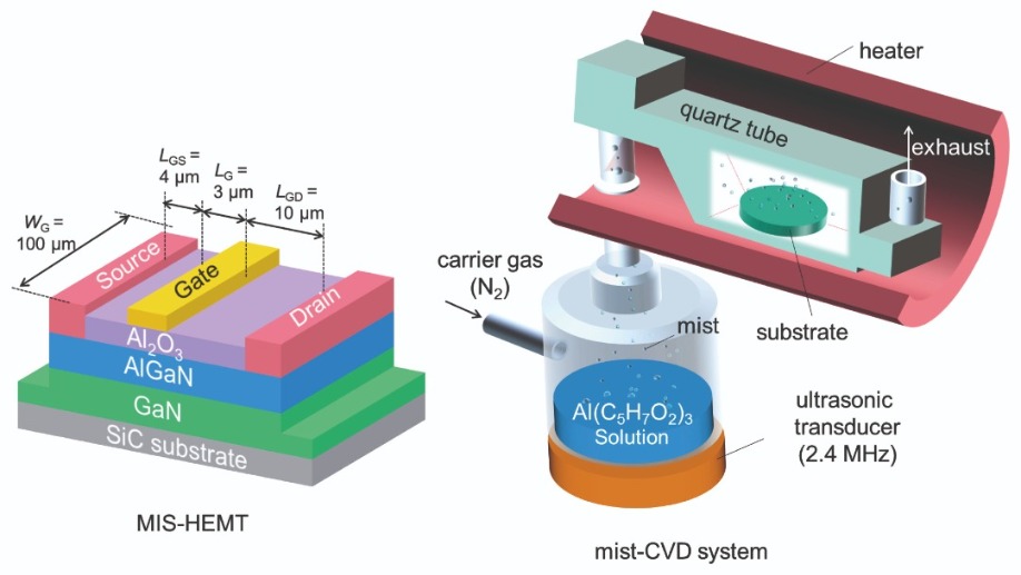
Mist CVD provides an environmentally friendly, low-cost approach to producing MIS-HEMTs.
R. S. Low et al. Appl. Phys. Express 14 031004 (2021)

