



HOW DO YOU MARK A MILESTONE? Many of us will take a look back, admiring how far we’ve come – while some of us will be more critical, evaluating what went wrong and how we could have done better. However, a milestone can also be a time to look forward, seeing what lies ahead and even setting some goals for the future.
In this issue of Compound Semiconductor, celebrating the 25th anniversary of this publication, you’ll find elements of all these approaches. We take a look back, covering what I believe to be the biggest story from each year, with reports on inventions of blue lasers, green lasers and blue VCSELs; commercial ventures ranging from the launch of satellites providing global cellular coverage to the debut of SiC diodes, SiC MOSFETs and
GaN FETs; and triumphs, such as the winning of a $10 million prize for LED lighting and the coming together of the world’s first compound semiconductor cluster. As the future of our industry is built on breakthroughs in the lab, we also showcase the best of innovation, picking the top ten research stories from the last 25 years.
Throughout last quarter of a century, my predecessors and I are indebted to you, our community, for supporting this publication with contributed features, interviews and the placing of adverts.
This edition is no different. Within its pages you’ll find a fascinating interview with Mike Krames, the pioneer of Auger recombination as the cause of droop, on how reaction to his work has evolved over the years. We also have a contribution from Aixtron on the evolution of its MOCVD tools; a piece from Cree co-founders John Edmond and
John Palmour on the company’s key successes over the last 25 years and more; a review from Asif Khan, the trailblazer of ultraviolet LEDs, on the big breakthroughs of this technology; and a feature from Robert Ploessl from Indium Corporation on the history of this crucial element.
We also look forward. We have a report on a project called Alterphasic, pioneering nanoscale SiC buffers that enable the growth of high-quality nitrides on a novel silicon-based template, and we take an educated guess at the roles our community might be playing in 25 years’ time.
So amongst all that content in this bumper issue I hope you’ll find something that interests you, as we mark 25 years of Compound Semiconductor magazine.
DRIVEN by increasing demand for innovative, self-emissive displays, global shipments of microLED displays are expected to soar to more than 16 million units by 2027, up from negligible levels in 2020.
MicroLED display shipment growth is being led by demand from the smartwatch and television markets, according to the MicroLED Display Technology and Market – 2020 report from Omdia.
Shipments of microLED displays to the smartwatch market are expected to exceed 10 million units in 2027, while shipments to the TV industry are expected to grow to more than 3.3 million units during the same year.
“Because of their superior luminance efficiency compared to rival organic light-emitting diode (OLED) displays, microLED displays are expected to become the next self-emissive display technology,” said Jerry Kang, associate director at Omdia. “Numerous startups, display manufacturers and consumer brands now are developing their own microLED displays, devices and process in various sizes, ranging from medium-to-large sizes to ultra-small dimensions.”
MicroLEDs represent an emerging flat-panel display technology that employs arrays of microscopic LEDs to comprise the individual pixel elements. Compared to conventional LCD displays, microLED displays can deliver superior contrast, faster response times and reduced energy consumption.
As mentioned, microLEDs also offer superior luminance efficiency compared with OLEDs. As a result, microLED technology is expected to emerge as a competitor to LCDs and OLED displays in applications ranging from wearable devices to televisions.
Several major technology players are taking steps to improve microLED technology and manufacturing.
Taiwanese firm AU Optronics recently introduced a prototype 9.4-inch flexible display using blue microLED pixels under red and green colour-conversion filters on low-temperature polysilicon plastic substrate.
Plessey Semiconductors announced it will help Facebook prototype and develop new technologies for potential usage in the augmented reality/virtual reality space.
Samsung Electronics in 2018 introduced a prototype TV with a chip-on-board processed RGB microLED display. The company plans to launch the product in 2020. Samsung Display has also started development of quantum dot nanorod LED technology, which applies nano-tube LEDs onto an oxide TFT glass substrate. Furthermore, many consumer brands are expected to release their own microLED displays or devices in the near future.
“The microLED market is poised for much more rapid growth once the technologies for manufacturing microLED chips – including mass transfer – gain more maturity,” Kang said. “The growing use of microLED display technology will push display makers to evolve away from current LCD and OLED display technologies.”
NAVITAS SEMICONDUCTOR has announced the delivery of its 5 millionth GaN power IC based on its GaNFast technology to OPPO, a fast-charge phone company.
Yingying (Charles) Zha, VP and general manager of Navitas China delivered the 5 millionth IC in the form of an award to Chang Liu, dean of the OPPO Research Institute, indicating OPPO’s affirmation
of Navitas’ GaNFast technology.
OPPO is described as a pioneer in the fast charging market, from the earliest and popular VOOC flash charging protocol, ‘five minutes to charge and two hours to talk’. The next-generation of SuperVOOC has increased the fast charging power of the mobile phone to 125 W. OPPO’s latest generation of lightweight fast-charge products
uses Navitas GaNFast power ICs to shrink up to 12 times compared with silicon-based chargers.
Liu said: “The cooperation with Navitas has perfectly matched the company’s continuous exploration and pursuit of new products, new materials, new processes and new technologies. We are excited to see Navitas’ company vision and excellent technology. We also hope to promote the development of GaN technology through in-depth cooperation and accelerate the commercialisation of the third generation of bandgap semiconductors.”
Zha said: “I am very pleased that OPPO, as a top mobile device manufacturer, has adopted fast charger technology based on GaNFast power ICs. Navitas’ GaN Power ICs with monolithic integration of GaN FET, GaN digital and GaN analog circuits can promote the commercialisation of a new generation of high-frequency, high-efficiency and very high-density power converters in a faster way.”

FOR ITS EXPANSION into the market for GaN-on-silicon high-power electronics and RF epi wafers, Azur Space relies on the AIX G5 + C from Aixtron, a provider of deposition equipment to the semiconductor industry.
Azur Space, a global leader in the development and production of multi-junction solar cells for space and terrestrial concentrated photovoltaic applications, is a long-standing Aixtron customer and has been using the AIX 2800G4-TM and AIX 2600G3 systems for its space solar application.
The now-ordered fully automated AIX G5 + C system featuring, in-situ cleaning, a cassette-to-cassette wafer handler and Auto-Feed Forward individual on-wafer temperature control, guarantees unmatched epitaxial stability and low defect densities.
Furthermore, Aixtron’s Planetary Reactor enables high increases in productivity and performance through highest throughput, lowest cost of ownership and highest yield performance. The state-of-the-art MOCVD platform is used for the production of 150 mm and 200 mm epiwafers.
With the establishment of a second business line leveraging its III-V manufacturing expertise, Azur Space positions itself on the fast growing market for GaN epiwafers for power electronics and RF applications. The demand for these epiwafers with its capacity to operate at higher frequency and in smaller form factor is mainly driven by
the need for energy efficient power systems, rapid charging solutions, renewable energies, server farms and the next generation of wireless networks.
“Market entry will be a challenge. However, our more than 25 years of experience in III-V epitaxy technology with development and mass production is ideally complemented by Aixtron’s system, so we have a very good starting position. Importantly, Aixtron’s Planetary Reactor provides us with the excellent quality level of our epiwafers required to capture the future market for high-performance electronics,” says Azur’s CEO Jürgen Heizmann.
Felix Grawert, president of Aixtron adds: “The market for GaN epiwafers for power electronics and RF applications is very exciting. It is expected to grow significantly driven by numerous applications such as fast charging solutions or the next generation of wireless networks. The high energy efficiency of GaN based power electronics contributes significantly to reducing the climate impact of new technologies”.
5G remains a hot topic in the smartphone market this year, as smartphone brands and mobile processor manufacturers, such as Qualcomm and MediaTek strive to expand their shares in the 5G market. According to the latest investigations by TrendForce, the Chinese government’s 5G commercialisation efforts have been particularly aggressive, leading the country’s 5G base station deployment and network coverage to each score first place in the global 5G industry.
As such, Chinese brands, which were ahead of their competitors in 5G strategies, occupied a 75 percent share in the global 5G smartphone market in the first half of this year.
TrendForce indicates that, aside from the various Android-based smartphone brands, Apple’s new models will also join the ranks of 5G smartphones. Given the total smartphone production forecast of 1.24 billion units in 2020, 5G handset production is expected to reach 235 million units, an 18.9 percent penetration rate.
Chinese brands are expected to occupy four out of the top six spots of 5G smartphone brands ranked by production volume
An analysis of the projected top six smartphone brands ranked by 5G smartphone production volume shows Huawei firmly sitting in first place. Huawei has shifted its focus to the domestic Chinese market under the impact of US sanctions and in preparation for China’s active 5G commercialisation efforts. The company is expected to produce about 74 million 5G smartphones this year.
Apple’s yearly 5G smartphone production is expected to total about 70 million units in 2020, which lands the company in second place. However, 5G functions will increase the production cost of smartphones accordingly. If Apple decides to directly reflect this added cost on the retail prices of the iPhone 12 series, it may lower its consumers’ willingness to purchase, in turn affecting the sales performances of the new iPhones.
Samsung has been experiencing setbacks in the Chinese market in recent years. Although these setbacks have not seriously affected its global market share and revenue, they have considerably slowed Samsung’s growth in the 5G smartphone market.
Samsung’s 5G smartphone production this year is forecasted at 29 million units, placing the company in third place globally. Vivo, OPPO (including OnePlus, OPPO, and Realme) and Xiaomi are tied for fourth place. As Huawei’s aggressive domestic expansion in the past few years has compressed the market shares of the three brands in the Chinese market, they have been actively focusing on increasing overseas market share to maintain their yearly production performances. Vivo, OPPO, and Xiaomi’s yearly 5G smartphone production volumes are projected to reach about 21 million, 20 million, and 19 million units, respectively.
Mid-to-low end 5G chipsets released by AP suppliers are expected to raise the penetration rate of 5G smartphones in 2021
TrendForce’s analysis of future developments in the 5G market shows that an aggressive push by mobile processor manufacturers will lead to the rapidly increasing presence of 5G chipsets in the mid-to-low end market, driving 5G smartphone production to surpass 500 million units in 2021, which will potentially account for about 40 percent of the total smartphone market.
Once 5G chip prices reach a stable level this year, smartphone brands may look to gain additional shares in the 5G smartphone market by sacrificing gross margins. In doing so, they are likely to accelerate the drop of 5G smartphones’ retail prices, and the market may see the arrival of 5G smartphones around the RMB 1000 price level ($1450) by the end of this year. Incidentally, it is worth noting that the penetration rate of 5G smartphones does not equal the usage rate of the 5G network, which depends on the progress of base station construction.
Since the current 5G infrastructure build-out is pushed back as a result of the pandemic, the global 5G network coverage will be unlikely to surpass 50 percent before 2025 at the earliest, with complete coverage taking even longer.
Founded in Taipei, Taiwan in 2000, TrendForce has extended its presence in China since 2004 with offices in Shenzhen and Beijing.
CAMBRIDGE GaN Devices Ltd (CGD), a spin-out from the University of Cambridge Department of Engineering, will lead a €10.3 million project dedicated to the design and development of the most energy-efficient next-generation GaN power modules.
Working alongside a consortium of 13 European partners with expertise across all aspects of power conversion, the GANEXT project, under the PENTA programme, will focus on producing prototypes for low and high power applications such as lighting, motor drives, converter blocks for renewable energies and on-board chargers for electric vehicles.
CGD develops highly efficient power electronics offering major energy savings in applications ranging from power supplies for consumer electronics to LED drives, data centres and wireless chargers. The company was spun out of the Department of Engineering’s High Voltage Microelectronics and Sensors Group in 2016, in order to develop GaN silicon substrate power semiconductors.
Giorgia Longobardi, CGD’s founder and CEO said: “The PENTA project creates a tremendous opportunity for CGD to engage with leading-edge companies in the area of power electronics. Not only will the project advance the knowledge in GaN technology and provide insights into its complex facets, but it will aim at delivering fully-working prototypes in lighting, motor drives, converter blocks for renewable energies and on-board chargers for automotive with record specifications and outstanding performance.”
Florin Udrea, CGD’s CTO and founder, said: “The quality of the PENTA consortium is remarkable and I have no doubt that we will deliver on the promises to make GaN technology a great success in the market. There is also a broader impact in adding our contribution to our ultimate quest for better use of energy resources and a cleaner environment.”
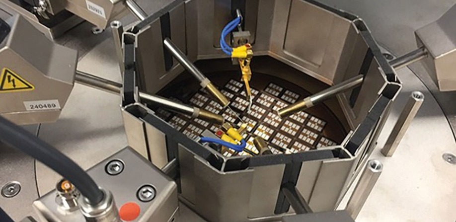
APPLIED OPTOELECTRONICS, a provider of fibre-optic access network products, has announced that production of laser diodes in July 2020 reached an all-time record of over 1.1 million units, nearly 65 percent higher than pre-Covid levels.
“AOI has been investing in capacity by adding additional production equipment, improving our manufacturing processes to increase yield and enhance quality, and adding staff,” said Thompson Lin, Applied Optoelectronics Inc. founder and CEO.
“The vast majority of our current laser production is 25G lasers which are in high demand now in our data center and telecom segments, including 5G wireless. This additional capacity will help us meet this increased demand. Having produced over 1.1 million tested and qualified lasers in the month of July is a significant step to achieve our near-term goal of producing 1.5 million lasers per month, which we expect to reach in Q4 of this year,” added Fred Chang, AOI’s SVP and North America general manager.
“Even more importantly, the significant improvements we’ve made in our manufacturing process have increased our manufacturing yield, which in many cases have also resulted in improved reliability that is critical for our customers.”
ADVANCED MICRO-FABRICATION EQUIPMENT INC. CHINA (AMEC), has launched the Prismo HiT3 system – an MOCVD tool engineered to mass produce deep-UV LEDs.
The system is the newest addition to AMEC’s portfolio of Prismo MOCVD products. With a maximum reactor chamber temperature of 1400 °C, the tool enables the growth of high-quality AlN and high-aluminium component material. Built for high throughput, the system can process up to 18 2-inch epitaxial wafers per run, with extendibility to 4-inch wafers.
Early customers include China-based Jason Semiconductor Co., Ltd. (Jason) a producer of deep-UV LEDs for home applications, medical instruments, and products used for scientific research.
Deep-UV light has been used for decades as a disinfectant for industrial and consumer applications. It works by disrupting the DNA of bacteria and viruses, and killing their reproductive capabilities. The emergence of pathogens like SARS, MERS, and Covid-19 has increased demand for deep-UV LED products with the wavelength power to destroy new microorganisms. Today’s state-of-the-art for this purpose is deep-UV LEDs at wavelengths of 260-280 nm like the products manufactured by Jason.
“Today, we’re seeing the benefits of deep-UV LEDs in real time with the technology now an important tool used to destroy harmful pathogens,” said Jian Kang, chairman at Jason. “As the science of DUV LED technology continues to advance, we are proud to operate at the leading edge with products to disinfect public environments, as well as the home. AMEC’s Prismo HiT3 system can meet the high-volume/low cost-of-ownership manufacturing imperatives for deep-UV LEDs.”
“The Prismo HiT3 system contains all the innovative features of our proven Prismo platform, now with new ultra-high-temperature process capabilities for AlN-based DUV LED applications,” said Zhiyou Du, executive VP and COO at AMEC. “an early user.

SWISS SOLAR START-UP Insolight has announced that a Series A round of just over €4.6 million has successfully been closed. The round was led again by Investiere, with co-investors Zürcher Kantonalbank, Swiss Immo Lab and a number of private business angels.
Following the first Seed Financing round in January 2018, Insolight has established a world record efficiency of more than 29 percent for flat solar panels, as certified by IES-UPM. The company has successfully taken the technology out of the lab and proved its robustness in real weather conditions. The Series A financing round – together with the €10 million HIPERION grant from the EU – will enable Insolight to start producing and selling the modules. The production will be outsourced to external manufacturers. Insolight is based at the EPFL Innovation Park in Lausanne.
Insolight’s technology is based on a patented optical technology and space-grade GaAs-based solar cells.
Insolight intends to sell its first modules to large solar energy corporates for applications in agrivoltaics. There is a unique potential for high efficiency and translucent modules to produce both solar electricity and crops on the land, whether deployed on fields or greenhouses. The nascent agrivoltaic market already represents 5 GWp of installed power with a market size estimated to nearly Ä700 million. It leverages unique advantages of the Insolight technology, differentiating the market entry strongly from mainstream products.
Rainer Isenrich, CEO of Edisun Power Europe AG and Alan Rosling (former executive director at Tata Sons) will remain members of the board of directors. The Insolight team is now on a mission to deliver the modules to the market. Insolight is supported by several programs from the European Commissions (H2020,Solar-ERA.Net, Eurostars, Climate KIC), national programs (Innosuisse, Innovaud, SPEI, FIT, VentureKick, CleanTech Alps), the European Space Agency (ESA BIC) and EPFL (Innogrant).
INFINERA has announced a succession plan to transition its leadership in the coming months. Tom Fallon will be stepping down as Infinera’s CEO and David Heard, the company’s COO, will be succeeding him.
This transition is expected to take place by the end of 2020 on a date to be determined. Fallon, in his 17th year with Infinera and 11th as CEO, will remain on the board of directors.
“I couldn’t be more pleased with the board’s selection of David as Infinera’s next CEO and I have the utmost confidence in his ability to successfully lead the company in its next phase of growth,” said Fallon, Infinera CEO. “When David joined Infinera three years ago, our objective was to bring onboard a COO who would be positioned to take over as CEO at the right time.”
“David’s contributions since joining the company have been substantial, making us more scalable as he led us through a major acquisition, driving synergies through operational improvements, aligning our product and service portfolio and focusing our investments on the highest value areas for our customers and shareholders.”
Having served as Infinera’s COO since October 2018 and led a publicly traded company as CEO in the past, Heard has over 25 years of industry experience in executive leadership roles that span a wide breadth of technology companies, including JDS Uniphase, BigBand Networks (now part of CommScope), Somera (now part of Jabil), Tekelec (now part of Oracle), and Lucent Technologies (now part of Nokia). He holds an MBA from the University of Dayton, an MS in management from the Stanford Graduate School of Business, where he was a Sloan Fellow, and a BA in production and operations management from Ohio State University.
In conjunction with this transition, Infinera is also announcing that Kambiz Hooshmand will be stepping down as chairman of the board on the same date as the CEO transition, while remaining on the board. Hooshmand has served as chairman since October 2010. George Riedel, a current member of the Board, will succeed Hooshmand as chairman.
“Together with the entire Board, I want to thank Kambiz sincerely for his longstanding and dedicated commitment and service to Infinera,” said Tom Fallon.
“We are very fortunate to have someone of George’s industry experience, knowledge and strategic leadership abilities step into the chairman role and partner with David as he assumes the CEO mantle later this year.”
“These succession changes have been thoughtfully planned and we anticipate a smooth transition. I am deeply appreciative of the opportunity to serve as CEO over the past decade and I look forward to helping Infinera in the next phase of our journey.”
US-BASED MATERIALS science researchers, led by Shui-Qing ‘Fisher’ Yu from the University of Arkansas, have demonstrated what they claim is the first electrically injected laser made with GeSn. Used as a semiconducting material for circuits on electronic devices, the diode laser could improve micro-processing speed and efficiency at much lower costs.
In tests, the laser operated in pulsed conditions up to 100 K.
“Our results are a major advance for group-IV-based lasers,” Yu said. “They could serve as the promising route for laser integration on silicon and a major step toward significantly improving circuits for electronics devices.”
The research is sponsored by the Air Force Office of Scientific Research, and the findings have been published in Optica, the journal of The Optical Society. Yiyin Zhou, a University of Arkansas doctoral student in the microelectronics-photonics program authored the article.
Zhou and Yu worked with colleagues at several institutions, including Arizona State University, the University of Massachusetts Boston, Dartmouth College in New Hampshire and Wilkes University in Pennsylvania. The researchers also collaborated with Arktonics, an Arkansas semiconductor equipment manufacturer.
The alloy GeSn is a promising semiconducting material that can be easily integrated into electronic circuits, such as those found in computer chips and sensors. The material could lead to the development of low-cost, lightweight, compact and low power-consuming electronic components that use light for information transmission and sensing.
Yu has worked with GeSn for many years. Researchers in his laboratory have demonstrated the material’s efficacy as a powerful semiconducting alloy. After reporting the fabrication of a first-generation, optically pumped laser, Yu and researchers in his laboratory continue to refine the material.
AT THE virtual International Microwave Symposium (IMS), Macom announced a new GaN-on-SiC power amplifier product line, which it is branding Macom Pure Carbide. The company also announced the introduction of the first two new products in the product line, the MAPC-A1000 and the MAPC-A1100.
“This new product line significantly enhances the capability of our existing RF power product portfolio,” said Stephen Daly, president and CEO. “GaN on SiC is a compelling technology and we are excited to begin offering our customers both standard and custom Macom Pure Carbide power amplifier solutions.”
The MAPC-A1000 is a high power GaN-on-SiC amplifier designed to operate between 30 MHz and 2.7 GHz and is housed in a surface mount plastic package. The easy-to-use general purpose amplifier integrates an input match which simplifies the customer’s design-in effort. The amplifier can deliver more than 25 W (44 dBm) at greater than 50 percent efficiency from 500 MHz to 2.7 GHz when tested in a circuit designed for operation over 2.2 GHz simultaneous bandwidth.
The MAPC-A1100 is a high power GaN-on-SiC amplifier designed to operate up to 3.5 GHz. The device is capable of supporting both CW and pulsed operations with output power levels of at least 65 W (48.1 dBm) in an air cavity ceramic package.
The two new general purpose amplifier products are ideal for use in avionics, high power mobile radios, wireless systems and test instrumentation.
Allos Semiconductors has sold its power electronics and RF business to focus on GaN-on-silicon epiwafers for microLEDs. Rebecca Pool talks to company co-founder, Alexander Loesing, to find out more
IN JULY THIS YEAR German GaN-on-silicon wafer developer Allos Semiconductors revealed that it had sold its high power electronics and RF business to Azur Space, a provider of III-V epitaxy for solar cells also based in Germany, for an undisclosed sum.
The move comes at a time when the market for GaN-on-silicon power and RF epiwafers is booming, and merger and acquisitions are rife. For example, just over a year ago, France-based Soitec bought GaN wafer supplier EpiGaN for Ä30 million to strengthen its GaN presence in the RF and power markets. Then in spring this year, STMicroelectronics made its mark on the power market when it acquired a majority stake in GaN innovator Exagan.
So why sell now? Clearly the timing works for Azur Space. As one of Allos’ co-founders, Alexander Loesing, says: “Azur Space has a manufacturing capacity of 500,000 150 mm wafers a year and wants to leverage its III-V epitaxy skills for the power market.”
“We see a second wave of power electronics businesses that don’t want to in-source GaN epitaxy,” he adds. “These companies require a reliable and capable source as they don’t want to spend time building up their own epi-supply, so this will be good for Azur Space.”
Allos also has mighty plans for expanding its microLED efforts. Minus its power and RF arm, the company intends to focus its resources on this market, which Loesing describes as ‘incredibly intensifying’. “We have three times as much work here than we did only a year ago,” he says.
Over the years, Allos has been building a compelling case for growing microLEDs on GaN-on-silicon wafers, instead of the industry stalwart, sapphire. But how exactly does the company intend to make its mark on the fast-growing, highly competitive world of microLEDs?
Making the difference
To reach mass sapphire-based microLED production, industry players are busy addressing manufacturability issues, including yield and cost. For example, GaN-on-sapphire LED chips are processed on 100 mm and 150 mm diameters. Larger wafers are too expensive to be used in LED manufacturing, and also suffer from bow, leading to lower yields.
Meanwhile, inhomogeneities in the emission wavelength of a typical GaN-on-sapphire LED epiwafer mean chips need to be tested and sorted into bins to ensure the microLEDs emit the desired colour. Given a 4K display comprises some 25 million microLEDs, this process of binning clearly isn’t viable at volume production.
“The industry needs to move towards an epi-growth and chip processing environment that delivers large diameters with a high uniformity to avoid the need for binning, and at high yields,” highlights Loesing. And the Allos director is sure that his company’s hetero-epitaxial GaN-on-silicon growth process will make the difference.
According to Loesing, the epi-growth process uses strain engineering and lateral overgrowth to overcome the lattice mismatch and thermal expansion differences between GaN and silicon that would otherwise lead to wafer bow, cracks, poor crystal quality, and associated wavelength non-uniformities and yield loss.
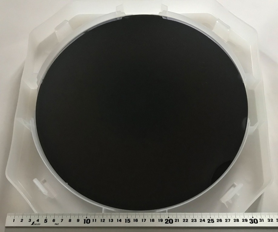
As part of the company’s method to achieve high crystal quality, epitaxial lateral overgrowth is used, which is analogous to the patterned sapphire substrates used in sapphire-based LED manufacture to reduce GaN crystal defects. Careful strain balancing introduced during epi-growth helps to control bow and deliver flat epiwafers after growth. And the company also uses its proprietary and patented strain engineering to precisely control heat across the entire wafer diameter during temperature-sensitive InGaN multi-quantum well growth, promoting wavelength uniformity and reproducibility from wafer to wafer.
“The strain engineering and crystal quality challenges are much more difficult in LEDs compared to power electronics, but this is good for us,” says Loesing. “Very few companies can use GaN-on-silicon to make LEDs with our levels of quality, and I haven’t seen anyone come close to the uniformities that we are showing.”
Indeed, at 2 x 108 cm–2, the defect density of its GaN-on-silicon substrates is on par with that of market-leading GaN-on-sapphire. Epiwafers are crack-free with minimal bow while wavelength uniformity is stable with nearly 98 percent of wafer areas hitting targets.
As Loesing also points out, silicon substrate removal via grinding and etching, as used in silicon lines, is more straightforward than the laser lift-off necessary to remove sapphire substrates from chips. And epi-growth takes place in standard MOCVD reactors on 200 mm and 300 mm wafers, opening the door to microLED production on low-cost, high yield, silicon processing lines.
Still, without a doubt the microLED world is very much entrenched in sapphire. To tackle tradition, Allos is working to ensure a steady supply of GaN-on-silicon epiwafers. “We need to make sure we can provide enough samples to our customers,” says Loesing.
Given time, the company director is confident that microLED players will make the move from sapphire to GaN-on-silicon. “If we’d spoken four years ago I would have said I don’t believe that the LED industry will ever take-up GaN-on-silicon as companies were focused on throughput,” he says. “But the arrival of microLED displays has changed this, and high yields are crucial to drive costs down – our technology ensures this with wafers, and all subsequent processing steps.”
So what now for Allos Semiconductor? Right now, the company is working on, as Loesing says, ‘results’.
Indeed, since the sale of its power electronics and RF arm, Allos has announced that it is working with researchers from King Abdullah University of Science and Technology (KAUST), Saudi Arabia, on high efficiency nitride-based red LEDs on silicon. Group head Kazuhiro Ohkawa from KAUST has already grown InGaN-based red LEDs on sapphire and working with Allos, intends to do the same on silicon.
“We continue to push forward and look forward to showing more results, and also to making new announcements about customer collaborations very soon,” says Loesing. “This microLED market is exploding and I’m having the most fun at Allos that I’ve ever had.”
Huge investment in South Wales-based CSconnected will bolster supply chains for worldwide markets. Rebecca Pool reports
WHILE THE WORLD WATCHES the coronavirus crisis unfold, many in the compound semiconductor industry are also alert to some exciting developments underway in South Wales. In June this year, the world’s only compound semiconductor cluster, CSconnected, was awarded a mighty £25.4 million in government funds to push the region’s home-grown technologies into the global marketplace and increase international trade in key sectors such as 5G and autonomous vehicles.
As Drew Nelson, Chief Executive and President of Wales-based epiwafer manufacturer, IQE, tells Compound Semiconductor: “An important aspect of this is to seek partnerships with other regions around the world and make contact with many other companies that may need to access [our technologies] and take part in this cluster.”
The funds will also be used to bolster the region’s existing supply chain so that products can be developed from concept to production, without outsourcing. According to Drew, the project is in its very early stages, but without a doubt, products for future technologies will be delivered.
“For example, we will be working on scaling up compound semiconductor production to include compound semiconductors on silicon for, say, 5G applications, and are looking towards getting some of these technologies onto a 200 mm platform – this is quite a big goal,” he highlights.
And as fellow cluster member, Wyn Meredith, Director of the Compound Semiconductor Centre, a joint IQE-Cardiff University venture to develop and prototype compound semiconductor materials, says: “We’ve been really focused on establishing a coordinated supply chain, in terms of materials, device fabrication and packaging, as well as capital equipment.”
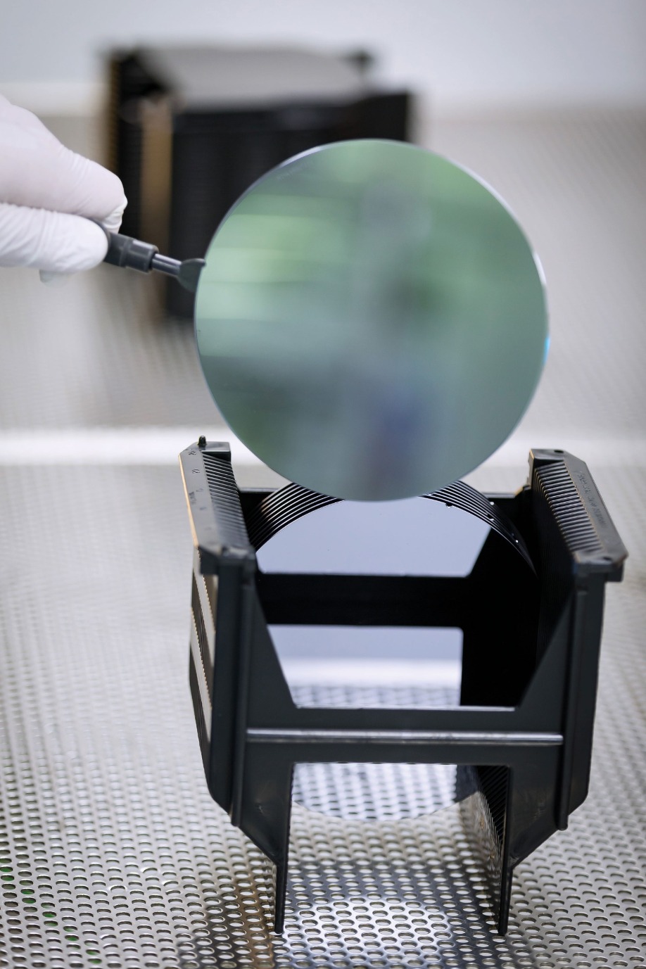
“We will now use this to build high-value added manufacturing,” he adds. “So we’ll be encouraging companies to settle in South Wales, help us to extend our supply chain and scale up compound semiconductor product manufacturing here.”
Building a supply chain
Since its inception in 2015, CSconnected has rapidly expanded to include a host of academic, industry and government partners that now constitute the largest concentration of compound semiconductor activity in the UK. As well as IQE, members include: the Universities of Cardiff and Swansea; etch and deposition process equipment supplier, SPTS; compound semiconductor and silicon foundry, Newport Wafer Fab; and chip maker, Microsemi.
Other key organisations include the Compound Semiconductor Centre, the Compound Semiconductor Applications Catapult, which focuses on research and product development, as well as UK-Welsh government investor, the Cardiff Capital Region City Deal, and Welsh Government.
To date, the cluster has secured more than £600 million in investments, provided around 1480 jobs, and accounted for at least £460 million of sales – with more than 90 percent relating to overseas exports, mostly EU destinations. And while all industry players occupy key places within the UK compound semiconductor supply chain – for example Newport Wafer Fab is the UK’s only silicon foundry, producing 200 mm wafers for silicon and compound semiconductors – industry can expect more players to join soon.
The latest £25.4 million funds come from the UK Research and Innovation’s Strength in Places Fund, and amount to more than half the £43.7 million project cost, with remaining cash provided by CSconnected members. The fund is designed to boost local growth, and current estimates indicate the project will create an extra 1160 jobs in the region come 2025.
At a time when UK industry has been left reeling from coronavirus, not to mention the anticipated effects of Brexit, these figures make welcome reading. As Meredith puts it: “We’re in a really interesting situation here – when most industries are thinking about how to get their staff off furlough and back onto permanent contracts so they can re-start manufacturing we’re thinking about expansion.”
The project is scheduled to start in October this year, so as Drew puts it, ‘precise details are still being worked out’. However, industrial cluster members are poised to lead four key programmes within the project.
Newport Wafer Fab, accompanied by Rockley Photonics, will head up the first programme aimed at developing foundry services for sensing and telecommunications. Meanwhile IQE will lead the second programme that will scale up GaAs-based photonics, including photovoltaics and pixel-based architectures, on large wafer formats. SPTS will head up the third programme that aims to expand capital equipment, including reactors, and in the final programme, Microchip is set to build a power electronics packaging pilot line.
“This is really about upskilling our supply chains and not leaving our infrastructure behind as we grow,” says Meredith.
“If we look at SPTS, for example, the company has always prided itself on using local supply chains in South Wales,” he adds. “This project can now help to grow these supply chains, many of which include SMEs or mid-size businesses, so SPTS can use and support these businesses rather than having to look further afield.”

Indeed, as Meredith also points out, a raft of academic-industry innovation work packages from the cluster are already underway and the businesses that take part will be able to feed into, and grow, future supply chains. Key UK-based industrial partners include measurement and motion control systems developer Renishaw, RF and power semiconductor player, Teledyne E2V, and steel-maker Tata Steel Europe.
“We’ve captured a lot of business here, and many of these guys don’t normally play in the compound semiconductor space,” says Meredith. “But this is deliberate – we are now engaging with companies at the far-ends of the supply chain that are becoming really enlightened to what we are doing.”
So what happens now? Clearly a critical mass of compound semiconductor activity is firmly in place in South Wales, and the latest funds will support more economic growth. As Meredith puts it: “We’re ahead of the game, but if you look at the value that is extracted out of our existing supply chains here, it’s miniscule compared to what we could be doing – our Strength in Places funds will provide a catalyst for this.”
And as the Compound Semiconductor Centre Director points out, more industrial expansion is coming soon.
“Who knows what post-Covid economic conditions are going to bring, and if there is a prolonged economic recession, research, development and innovation budgets are going to come under a lot of pressure,” says Meredith. “But we’ve now got ours ring-fenced for the next four-and-a-half years, so can effectively proceed as we wanted to do pre-Covid.”
With a pedigree dating back to the early 1980s, Aixtron has spent several decades at the forefront of MOCVD equipment manufacturing
BY MICHAEL HEUKEN FROM AIXTRON
BACK IN 1995, when Compound Semiconductor magazine made its debut, Bill Clinton presided over the United States, owners of PCs could start getting their hands on Windows 95, and our industry was far, far smaller than it is today.
Reflecting its diminutive size was its lack of diversity. This is illustrated by the narrowness of the discussion that took place at the 8th ICMOVPE, held in Cardiff in 1996, where delegates pondered the question “MOVPE – Is there any other technology for optoelectronics?”. Back then the manufacture of red and infrared LEDs was well established, but the blue cousin had only just been invented; volumes of GaAs HBT production were tiny, due to very few owners of mobile phones; III-V solar cells were yet to establish themselves as the dominant technology for powering satellites; and the manufacturer of InP lasers and photodetectors to build the information superhighway provided a substantial proportion of total industry revenue.
Although the compound semiconductor industry was in its infancy back then, manufacturers of optoelectronic devices did not have to rely on home-built systems for MOCVD growth. They also had the option of purchasing commercial reactors.
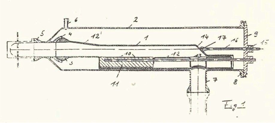
Figure 1. On the 30 June 1987 Aixtron co-founder Holger Jürgensen and his colleague Meino Heyen filed a German patent for the invention of a horizontal tube reactor, later marketed as Aixtron 200. This patent, published on 12 January 1989, details a round outer tube and an inner rectangular liner tube. The design allows an easy exchange of the liner, aiding cleaning. The susceptor is positioned parallel to the gas flow. In the patent there is a diagram of the reactor, shown above, and labelled: (1) inner rectangular quartz reactor, (2) round outer quartz tube for protection, (3) flange with spherical connector, (4) flange to pick up the connector of the rectangular quartz reactor, (5) gas inlet for process gases, (6) purge gas inlet, (7) exhaust, (8) reactor port seal, (9) reactor port for loading and liner tube exchange, (10) wafer, (11) susceptor as wafer carrier, (12) quartz plate to maintain laminar flow, (13) exhaust opening, (14) reactor end to optimise flow, (15) screw joint to adjust the liner tube with the push rod, (16) push rod, and (17) fixing for the push rod.
As far back as the 1980s, we had started to consider the limitations of our first commercial reactors, the Aixtron 200 series (see Figure 2, 3 and 4. The latter shows a typical reactor from the Aixtron 200 series, the Aixtron 200/4 system, which features heating with a standard lamp or an RF heating system, a glove box and computer control.). Reactors in the Aixtron 200 series had been prototyped at RWTH, prior to further development and commercialisation by our team. This MOCVD system had a great reputation within the research community, thanks to its combination of simplicity, reliability, versatility and ease of use.
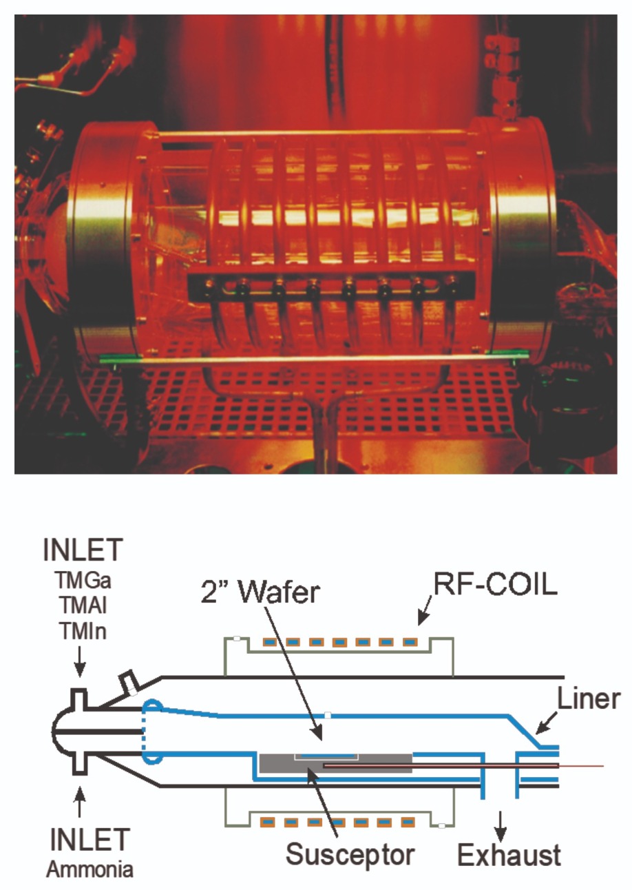
Figure 2. (a) A horizontal tube 200 reactor with water cooling, suitable for high-temperature growth. The RF coil allows heating well above 1000 °C, enabling the growth of III-N based materials. (b) A diagram of the 200 reactor, showing the holes in the liner tube. The transparency of these quartz reactors provided some of the first in-situ monitoring during growth.
A severe limitation of the horizontal tube reactor is its side walls. When they are hot heterogeneous reactions take place; and when they are cold condensation forms. Another impediment is that the side walls consume source material, impairing the efficiency and the uniformity of the reactor. The side walls also alter the flow pattern perpendicular to the gas flow direction, making the growth of high-quality epilayers more difficult.
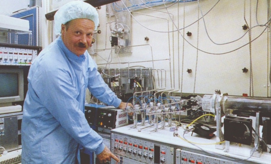
Figure 3. Holger Jürgensen, co-founder of Aixtron, operating one of the company’s first prototype reactors, used at that time for the growth of InP materials at RWTH Aachen University. The early work was undertaken in co-operation with D. Grützmacher, today professor at FZ Jülich. The image shows the quartz reactor, early versions of the vent run system and so-called read out boxes to set the mass-flow control (MFC) readings. Fans under the reactor were switched on in the cool down phase to decrease cool down time and increase productivity. Picture from late 1980s.
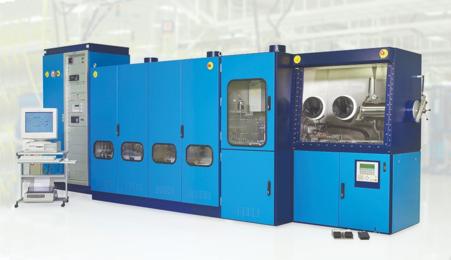
Figure 4. Standard lamp-heated Aixtron 200/4 system with the typical blue colour, glove box and computer control. This reactor was used primary for growing GaAs- and InP-based material systems. One wafer up to 4 inch fits into the reactor.
Planetary Reactor
Demand for compound semiconductor devices continued to rise throughout the 1990s and beyond. We responded with the introduction of our Planetary Reactor series, which uses two forms of circular motion to ensure the uniformity of many wafers in a reactor. Every wafer rotates around the centre of the reactor, and clusters of them also circulate around their own local centre (see Figure 5).
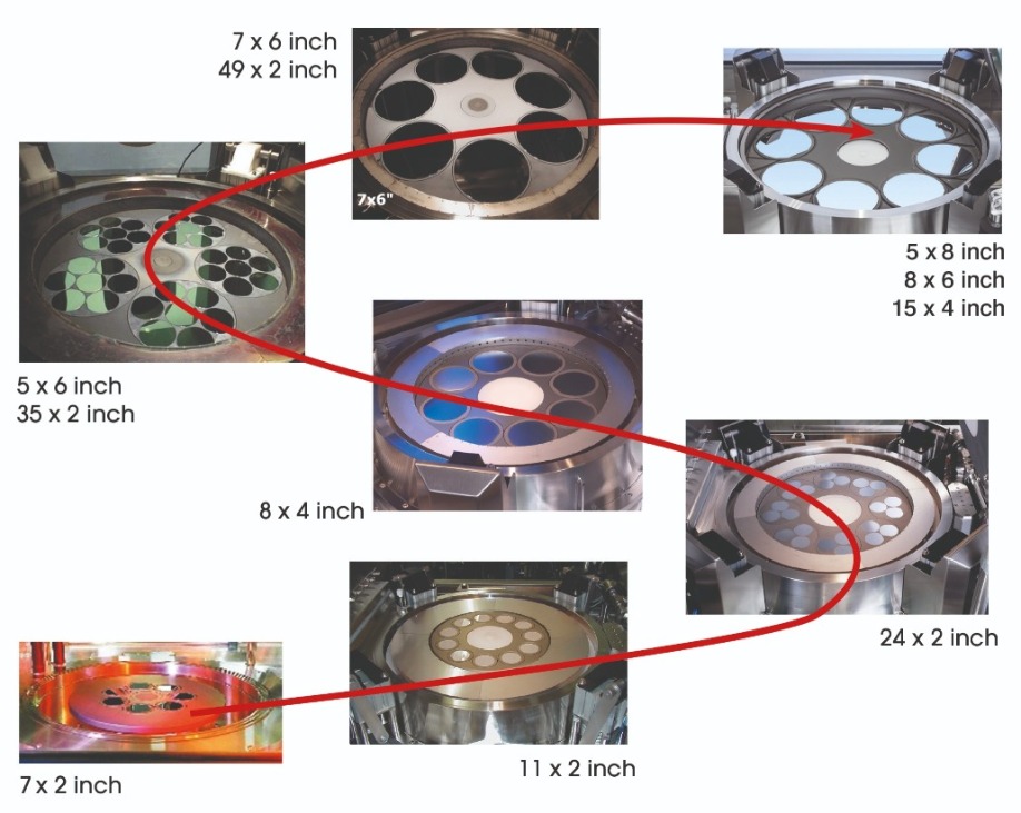
Figure 5. The evolution of the Planetary Reactor family for the growth of III-N material. Based on simulation results, reactor chambers became larger, accepting more and larger wafers, while simultaneously improving uniformity and reducing material consumption per wafer area.
The Planetary Reactor has many merits. It is a horizontal reactor which is free from side walls, and the temperature of its top wall, also known as the ceiling, can be controlled to make it passive. This type of reactor can ensure excellent, controllable uniformity, making it ideal for large scale production. It is also renowned for its: high precursor utilisation efficiency; its low maintenance requirements; its accommodation of large wafer areas; the opportunity it provides to use automated cassette-to-cassette loading systems; and its high growth rates – values of more than 30 μm/hr. Thanks to this great set of attributes, our Planetary Reactors provide low-cost, high-volume, multi-wafer production using multiple wafers up to 200 mm.

Figure 6. The 1995 Aixtron top management team: Dr. Holger Jürgensen and Kim Schindelhauer. They are looking into the Planetary Reactor of the 3000 series developed for large-area, GaAs-based solar cells.
In the 2000s, the increases in yield that drove the cost reductions that are shown in Figure 10 came through accommodating a larger wafer area in the reactor, while keeping uniformity as high as possible. Launched in 2001, our third-generation Planetary Reactor for GaN, the AIX 2400 G3, had a capacity of 11 2-inch wafers. Upgrading this the following year led to the introduction of the AIX 2600 G3, which could accommodate 24 2-inch wafers. By 2006, we could house 42 2-inch wafers, thanks to the launch of the AIX 2800 G4 HT, a fourth-generation GaN Planetary Reactor. The first fifth-generation GaN Planetary Reactor followed in 2009, enabling growth of 8 6-inch epiwafers in a single run. During the last decade increases in productivity have not come from increases in wafer capacity, but from other strategies that trim cycle times, such as the introduction of automated wafer-loading systems.
We have been working on wafer loading for many years. Back in 1996 we developed the first automated MOCVD reactor, featuring a spider-like robot for loading wafers into a cassette. By avoiding the need to cool wafers to room temperature, this handler cut cycle times by up to 30 percent, increasing throughput.
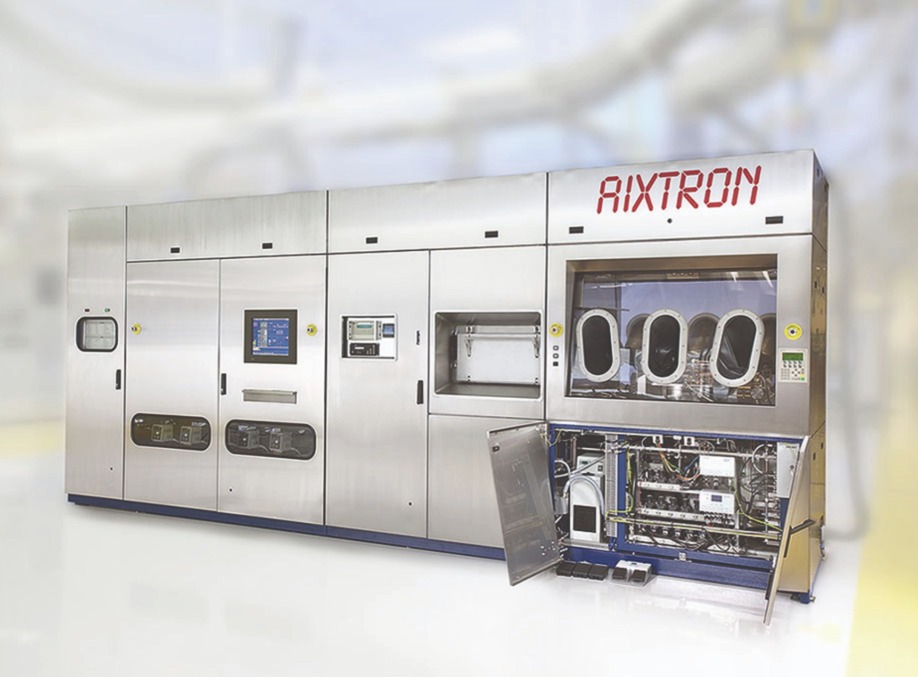
Figure 7. The Planetary Reactor in the integrated concept design. Beside productivity improvements, the stainless steel outlook approaches silicon fab style.
A significant refinement to our reactors came in 2012 when we replaced our conventional, triple injectors with variants featuring five injectors. These ‘penta’ injectors brought knew tuning potential to widen the process window for best uniformities up to 200 mm wafer size.
Another aid to the process engineer has been the introduction of optical in-situ monitoring tools. This form of instrumentation opens the door to advanced process control. It enabled logging and control of far more data, including values for wafer bow, growth rate and local on-wafer temperature. By designing reactors that accommodate an optical path to the growth surface, we established emissivity-corrected pyrometry that provides measurements of on-wafer temperature. Armed with this insight, process engineers can now realise wafer level control and optimise their epitaxial yield.
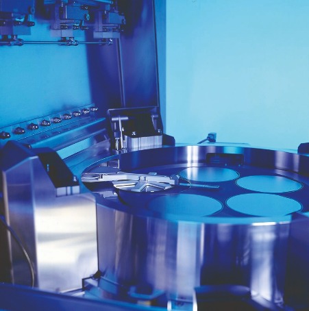
Figure 8. View in an AIX 2600 G3 Planetary Reactor equipped with a wafer loader as delivered in 1996.
In addition to our portfolio of Planetary Reactors, we offer those that are based on a Closed Coupled Showerhead design. This alternative reactor architecture, developed in parallel, also offers proven production capability. We offer this design to cater to those customers that are more familiar with the Closed Coupled Showerhead reactor and want to continue to produce epiwafers with this technology.
The Closed Coupled Showerhead
Like our Planetary Reactors, within the suite of Closed Coupled Showerhead designs, throughout the first decade of this century increases in wafer capacity led to breakthroughs in productivity. In 2001 and 2002 we launched reactors for nitride growth that accommodated 6 and then 19 2-inch wafers, and we followed this up with the introduction of the Crius, Crius II and Crius II XL in 2006, 2011 and 2012 – they housed 31 2-inch wafers, 55 2-inch wafers, and 19 4-inch wafers, respectively. In 2015, we introduced a semi-automated reactor with an even larger chamber, capable of producing 31 4-inch epiwafers in a single run. With this class of reactor, growth rates of even up to 280 μm/hr were demonstrated.
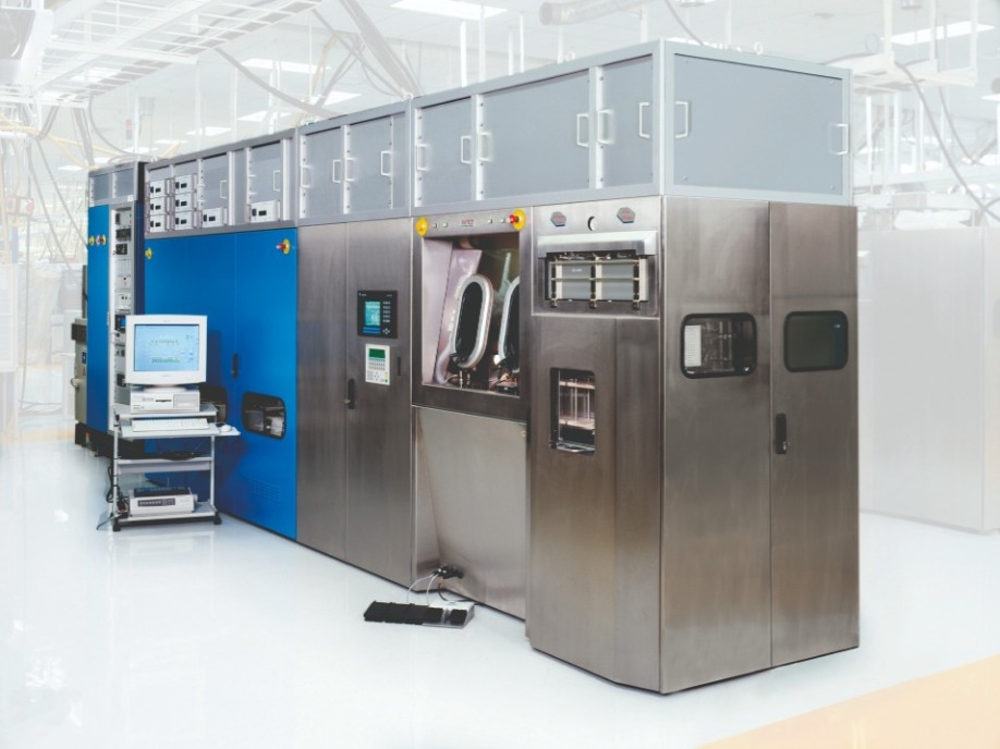
Figure 9. An early Planetary Reactor.
We decided to focus on our strength, which is providing the growth technology for producing high-tech devices that demand advanced MOCVD capability. For engineers that are producing lasers, III-V solar cells, advanced transistors, microLEDs for displays, and high-speed InP-based lasers for telecom and datacom networks, our Planetary Reactors are a great choice, combining a high level of performance with excellent yield and productivity. The Close Coupled Showerhead remains the solution of choice for R&D systems or for single systems that then require superior performance once again – which a vertical batch reactor can inherently not deliver well.
For the last quarter of a century, we have focused on ways to enhance productivity. This has been accomplished through the likes of increased reproducibility, superior layer uniformity, wafer level automation, and the introduction of in-situ metrology that enables the acquisition of process data, key to smart system control and predictive maintenance.
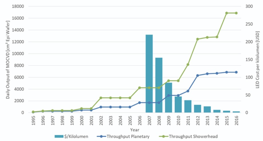
Fig. 10: Progress of MOCVD productivity and cost/kilolumen, based on United States dollars. Calculations used Aixtron estimates and data from https://archive.thinkprogress.org/5-charts-that-illustrate-the-remarkable-led-lighting-revolution-83ecb6c1f472/ The leaps in performance of the Planetary Reactor are due to: the introduction of the 3rd Generation GaN Planetary Reactor AIX 2400 G3 (11 x 2-inch) in 2001; an upgrade to the GaN Planetary Reactor AIX 2600 G3 (24 x 2-inch) in 2002; the launch of the 4th Generation GaN Planetary Reactor AIX 2800 G4 HT (42x2 inch) in 2006; the introduction of 5th Generation GaN Planetary Reactor AIX 2800 G5 HT (8 x 6-inch) in 2009; the implementation of semi-automated wafer loading in 2011; and the switch to a penta injector, for the 5 x 8-inch configuration in 2012. Between 2010 and 2015, additional improvements came from CIP continuous improvement programmes, and the development of chamber in-situ clean. For the closed-coupled-showerhead, productivity gains came from: the introduction of the 6 x 2-inch nitride reactor in 2001; an increase in capacity to 19 x 2-inch in 2002; launches of the Crius, Crius II and Crius II XL in 2006, 2011 and 2012, that had chambers accommodating 31 x 2-inch, 55 x 2-inch and 19 x 4-inch wafers, respectively; and the introduction of the AIX R6, 31 x 4-inch reactor in 2015.
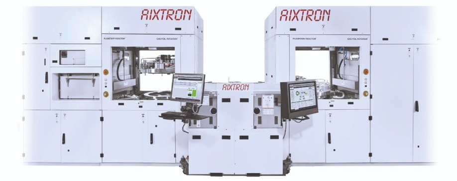
Figure 11. The latest (2020) G5+ C dual Planetary Reactor module cluster featuring cassette-to-cassette wafer handling.

A silicon template with an incredibly thin SiC buffer layer looks set to revolutionise a range of high-performance GaN-based devices, including deep-UV LEDs and GaN HEMTs
BY Dmitry Khmyznikov, Co-founder of THE Alterphasic project AND Alexey Redkov, Senior Researcher of Alterphasic R&D team
Our industry uses silicon substrates as the foundation for manufacturing several different devices. Transphorm employs it as the bedrock for its GaN FETs, now numbering more than 500,000, and Toshiba uses it for producing GaN-on-silicon power devices. Silicon substrates also feature in microLED displays made by Plessey, and in LEDs developed by both Samsung and Bridgelux, now part of Toshiba.
There are many reasons why these chipmakers use silicon as the foundation for device production. Silicon substrates are low in cost, widely available, and allow processing in 200 mm silicon lines, which may offer very competitive production costs, while employing tools with greater levels of performance than those found in many compound semiconductor fabs.
However, producing high-quality devices using silicon is far from easy. The main issue is the significant lattice and thermal mismatch between the nitrides and the substrate. These differences induce stress and strain in the epilayers, causing wafers to bend, bow and even crack. Strain management is essential, as wafers must be flat to within several tens of microns to enable processing in silicon lines.
One way to ensure flat enough epiwafers is to introduce buffer layers that manage stresses and strains. However, this is not easy to do. Successful buffers are complex, requiring years of development. What’s more, their formation often involves depositing many layers, adding to the material costs of the epiwafer, as well as overall production costs, increased by longer growth times. Even with thicker buffer layers, dislocations are present throughout the heterostructure, hindering device performance. Yet another drawback is that the buffer may hamper thermal management, because it can increase the distance between the location of heat generation and any heat spreading technology.
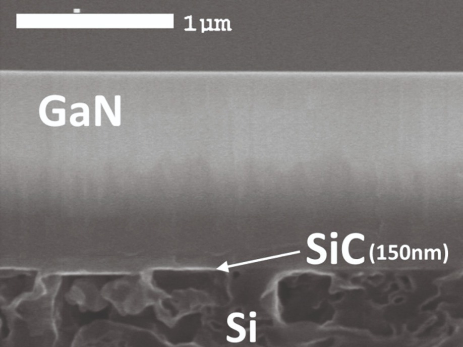
A very thin film of SiC enables the growth of high-quality GaN on a silicon substrate. The key to this success is the use of a nano-assembly method that converts a very thin layer of silicon into both cubic and hexagonal SiC.
Turning to nano-assembly
Our technology does not involve conventional film growth, with materials deposited from above. Instead, we replace silicon atoms in a special way that retains the original crystal structure of the silicon matrix. Using this ‘nano-assembly’ method, we ‘convert’ a very thin layer of silicon into both cubic and hexagonal SiC.
During this process, we form a special porous buffer layer beneath the SiC. The top nano-SiC layer that is created provides the ideal foundation for the growth of III-Ns, thanks to the compatibility of its properties with the crystal structure of nitride heterostructures.
When epitaxial films are grown on our silicon-based templates, mechanical stress relaxation takes place. This is driven by the preliminary embedding of the substrate lattice through assembly of nano-objects. By ensuring that carbon atoms are positioned at interstitial positions of silicon and silicon vacancies, we create a so-called ‘dilatation dipole’.
Unlike traditional epilayer growth, the orientation of our films is determined by the crystal structure of the original silicon matrix, rather than just the substrate surface. We have found that the best way to produce a cubic crystal is to form a dilatation dipole that is perpendicular to the (111) plane of silicon. When this occurs, almost all the elastic dilation energy of the film relaxes due to dipoles alone, leading to high-quality SiC films.
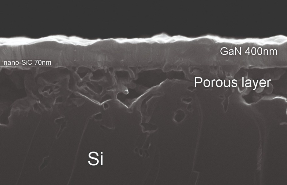
A high-quality epitaxial layer of GaN is gown by HVPE on a hybrid nano-SiC-on-silicon substrate.
To demonstrate the promise of our technology, we have used it to produce a wide range of thick, single-crystal, low-defect layers of various III-Ns using HVPE. This includes conventional GaN, AlN, AlGaN, and also a variety of semi-polar forms of GaN. Examples of nano SiC-on-silicon substrates that we have made, reproduced and tested in the lab include: AlN layers with an orientation (0001) and thicknesses ranging from just 40 nm to 700 μm, using silicon orientations (111) and (011); and semi-polar epitaxial AlN layers with the orientations (1120), (1013) and (2023), using silicon orientations (001) and (310).
Additional results include the growth of AlGaN layers with a (0001) orientation that have thicknesses between 100 nm and 400 μm, formed using SiC-on-silicon (001) substrates. We also separated layers with a thickness of 400 μm from the template.
Using our technology, we have produced a portfolio of monocrystal layers that are completely free of cracks. As well as AlGaN layers with a thickness up to 400 μm that we have just mentioned, we have made AlN with a thickness up to 300 μm, GaN with a thickness up to 200 μm and semi-polar (1124) GaN.
We have determined the growth rates for a variety of III-N films grown on our SiC-on-silicon templates, using the growth conditions detailed in Table 1, and layer thicknesses determined by electron microscopy. Films of GaN, AlGaN and AlN had thicknesses of 2.2 μm, 1.82 μm and 0.72 μm, respectively, while the SiC layer is just 70 nm-thick. This implies a growth rate for a GaN layer of 66 μm/hr, that for an AlGaN layer of 36 μm/hr and that for AlN of 42 μm/hr. The growth process still can be further optimized for higher growth rates.

A range of high-quality, thick films of III-Ns can be grown on Alterphasic’s nano-SiC-on-silicon substrates using HVPE.
Simple substrate separation
For some devices, such as UV LEDs, it can be useful to remove the silicon substrate, as this can absorb light and hold back efficiency. Thanks to the porous layer between silicon and the incredibly thin layer of SiC, we can employ a very simple chemical etching process, taking a matter of minutes, to separate the thin films or heterostructures from the silicon substrate. The freed material can provide a foundation for further bulk crystal growth, or be attached to another substrate.
Many devices could benefit from the high-quality, III-N layers formed with our silicon template technology. Our breakthrough could aid the manufacture of III-N transistors, as well as visible and UV laser diodes, LEDs and VCSELs. When these optoelectronic devices are grown on the conventional planes of III-Ns, efficient radiative recombination is hampered by strong internal electric fields. Switching to the semi-polar planes we have produced alleviates this, unlocking the door to more powerful light emitters.
To demonstrate the capability of our technology at the device level, we are using our SiC-on-silicon templates as a foundation for HEMTs and deep UV LEDs. For the latter, we start with a layer of AlGaN. We see this as a better choice than AlN, a material that seems incompatible with reasonable levels of p-type doping. Even in layers of AlGaN, realising p-type doping is a challenge, due to the high ionization energy of acceptor impurities. Efforts on this front are also hampered by the strong interaction of acceptor impurities with various structural AlGaN defects, leading to the formation of deep levels associated with both acceptors and donors. This work is still in its infancy, with successes to date including the fabrication of AlGaN layers with an aluminium content close to 50 percent.
Such efforts are showcasing the capability of our novel templates, and their capability to transform the production of various wide bandgap electronic and optoelectronic devices that benefit from increased material quality. Costs of chip production should also plummet with our templates, due to a drastic reduction in the cost of growth of these structures, a significant simplification of the growth technology, and the scalability on offer by turning to substrates with large diameters.
Further reading
S.A. Kukushkin et al. J. Phys. D: Appl. Phys 47 313001 (2014)
S.A. Kukushkin et al. J. Appl. Phys. 113 024909 (2013)
Mike Krames, leader of the team that identified Auger recombination as the cause of GaN-based LED droop, discusses his early work on this topic, his views on related experiments, and how this malady impacts green and ultraviolet LEDs
BY Richard Stevenson
RS: When you led the team at Lumileds’ Advanced Laboratories, you started looking at the potential causes of droop in the early 2000s. How did this work unfold?
MK: We first thought there was a current-injection problem. We put together a team, and within less than a year of measurements we knew we had something else.
We started to pare back the problem. Rather than electrical injection, we would just excite carriers in the active region and see what happened. I authorised Gerd Mueller, who was in my group, to put together a selective excitation optical measurement tool. This set-up required a very expensive tuneable laser, which produced very high power pulses. Gerd got that up and running and we started to inject photo-carriers directly into undoped structures. By 2004 – or 2005 at the latest – we had what looked like Auger recombination. We would directly photo-inject carriers, raise the carrier density and see the light output roll off and lifetime shorten.
Later on we carried out one of the critical experiments that proved leakage plays no role whatsoever. Aurélien David carried out a closed-circuit, reversed-biased LED experiment. He photo-injected carriers and looked for leakage. When he increased photoexcitation into the Auger regime there was no observed increase in leakage current at the terminals. So it couldn’t be leakage – it had to be recombination happening within the active region. So we had very strong evidence that it was an Auger-like process.
RS: In early 2007 Lumileds issued a press release saying it had fundamentally solved droop, but did not divulge the details. In the months that followed, did you personally get a lot of enquiries from people asking for more information?
MK: We did, and frankly a little bit of flack as well. ‘Fundamentally solved’ was marketing language and frankly something I was not thrilled about. But I stopped short of escalating to the CEO and saying ‘over my dead body’.
What we did know is that we had a fundamental understanding of droop that we believed later would be proven. Droop is not something that is solved, because Auger recombination is a band structure phenomenon. If you have a carrier density of a certain level, you have Auger carriers. And so every commercial GaN-based LED today has some Auger loss.
RS: Later in 2007, at the International Conference on Nitride Semiconductors in Las Vegas, you presented the details on the cause of droop. What was the reaction?
MK: It was a really charged atmosphere when we walked the floor. The notion of Auger recombination having a meaningful effect in wide bandgap semiconductors was not known – was frankly not even considered. If you look at Shuji Nakamura’s book on the blue laser diode, and Joachim Piprek’s estimates of the coefficient, Auger recombination was considered to be negligible. Auger had been ignored by the GaN community. And here we were showing that not only can you not ignore it – that it is the number-one cause of loss in high-performance LEDs at the current densities we like to run at.
A lot of people were like ‘wow, really’, and some academics probably thought they should have discovered this first. Frankly, there were some who just couldn’t believe it. A lot of the academics feel that they should be leading the way most of the time, but industrial researchers, when they get on to something can move the needle quite a bit, and that’s certainly true in LEDs.
I should point out that just because Auger recombination is the main, dominant mechanism, it doesn’t mean that you can’t have a leakage current problem. You can have a bad diode. You get that in academia a lot. You see from papers when diodes are not well designed. It’s hard to optimise an LED: you have to have very good control over growth, interfaces and doping; and you have to do it just right. If you get any of that wrong you are going to see leakage.
The point is that for the optimised structures that Lumileds is growing, Osram is growing, Nichia is growing and Cree is growing, you don’t have that problem. You have rollover not from leakage, but from Auger recombination.

Mike Krames has kept in good touch with his PhD supervisor Nick Holonyak, Jr., who is the inventor of the LED and led a group at the University of Illinois at Urbana Champaign. Here, Krames is making a visit during his time as leader of Lumileds’ Advanced Laboratories.
RS: Has your understanding of droop led to better devices?
MK: At Lumileds we reduced droop quite a bit. In 2015, I used my understanding of Auger at Soraa to make, what I believe, are the world’s best LEDs ever published. Operating in the violet, these devices had an 84 percent power conversion efficiency. That’s a far cry from where almost all LEDs are, even today.
The structures we used at Soraa were very, very highly optimised. We reduced the carrier density as much as we could – you can’t too much or you’ll end up in the Shockley-Read-Hall regime – but the peak efficiency for these diodes was at a pretty healthy tens of Amps-per-square-centimetre. We operated these devices up to 200 Amps-per-square-centimetre in lighting products.
RS: Several research groups working on droop have questioned the validity of the ABC model to fully account for the behaviour on an LED. What are your thoughts on this matter?
MK: There are different versions of the ABC model. It’s easy to poke fun at it because it is simple, and I think academics don’t like it because it is too simple. The truth, though, is that if you have structures where leakage is negligible – and that’s true for very high quality, optimised LEDs in GaN – then the ABC model fits the data quite well.
You need to account for the fact that each of these terms has some carrier density dependence. So if you mean the ABC model as purely A is a constant, B is a constant, C is a constant, the fit is not going to be so great. But you can get an extremely good fit if you use an adjustable version that is carrier-density dependent. For example, you use a biomolecular radiative rate that reduces a little bit due to phase-space filling, and you have some linkage between A and C, because Auger rates are influenced by defect scattering.
If you have leakage, or something else, you need to add additional terms. But from a practical view, for those of us who are leading the industry in LED development, the ABC model has been very useful.
Martin Strassburg and colleagues at Osram Opto Semiconductors used the ABC model quite effectively as a very simple way to estimate internal quantum efficiency, by just measuring the shape of this curve. Trying to measure absolute quantities is extremely difficult, so if you have a trick that enables you to do it faster and simpler, that’s really powerful.
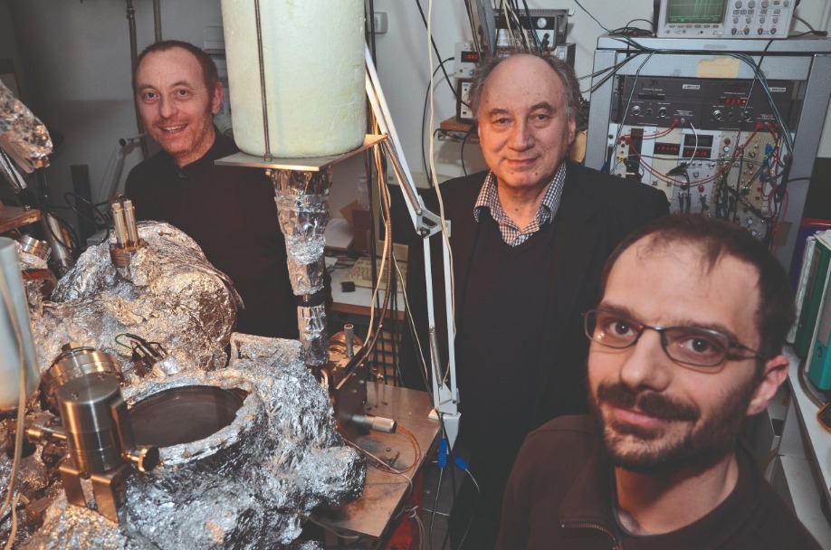
Mike Krames (bottom right), leader of the Lumileds Advanced Laboratories, put together a team from scratch that eventually numbered around 40 researchers.
MK: Chris Van de Walle at the University of California, Santa Barbara, did some first-principles calculations to show that defect-mediated or alloy-scattering-mediated Auger recombination could happen in InGaN and result in Auger coefficients of the order we were measuring. That was helpful, because it got the theoretical community involved in thinking about how we could attribute our findings.
RS: In the Spring of 2013, Claude Weisbuch’s team at the École Polytechnique in France, working with researchers at the University of California, Santa Barbara, claimed they had irrefutable evidence for Auger as the cause of droop. This team injected carriers into the quantum well and recorded both the light emission and the energy of electrons exiting the device through the p-side. At higher currents they detected higher energy peaks associated with vacuum-emitted electrons, and argued this could only be caused by Auger electrons. Do you, like this group, see this experiment as the ‘smoking gun’?
MK: Yes, very much so. This work showed hot electrons coming off the surface of the LED. How do the electrons get all that energy? Auger scattering is by far the most likely process. The fact that they saw the increase in the hot carriers right around the point that you start to see the rollover is too much to be a coincidence.
RS: Has there been any important work on droop in the last few years?
MK: Aurélien David, who came to Soraa from Lumileds after me, has done some really nice work on the details of recombination processes in InGaN. He considered the Auger process in more detail – whether it’s an electron-electron-hole process or an electron-hole-hole process, and whether the Auger scattering increases with defects, which it seems to. His work is, for me, the most clear assessment. He takes into account all the different recombination and traffic pathways, on materials that are very, very high quality, so you get the cleanest picture of what is going on.
By simultaneously measuring light emission and the energy of hot electrons, researchers led by Claude Weisbuch, from École Polytechnique, France, offered a new way to observe the behaviour of carriers in LEDs. Mike Krames has a very high opinion of this work, which provides further evidence that Auger recombination is the cause of LED droop
RS: Have there been any papers published that have made you reconsider your views on droop, and led to a few sleepless nights?
MK: No. There’s been a lot of interesting work around alloy fluctuations, especially for high indium-nitride mole fraction LEDs, like green LEDs. Some groups were arguing that alloy fluctuations cause droop, not Auger. But the issue is that there has to be some loss mechanism for the carriers, as otherwise they are going to hang out until they recombine. You then get back to Auger.
RS: My impression is that within the community that has studied LED droop, the vast majority of researchers, regardless of what they postulate, are tending to take an entrenched position. Will it take a new generation of researchers, approaching this topic with an open mind, to bring the debate on droop to
an end?
MK: It’s possible that my views are skewed, but I don’t see this debate. At least, for those whose life depends on the performance of these devices, it’s quite clear what the issue is. It’s a tough problem, and that’s why we still have droop in these LEDs. It would be quite ironic if we had a current leakage problem that the entire GaN community in the world over ten years, with billions of research spent, couldn’t have solved. The problem is bigger than us – it’s Mother Nature, it’s the band structure that allows this to happen.
RS: Has it been necessary to combat droop to drive LED lighting forward. Or has the overcapacity in the LED market, and the tumbling price of these chips, had a bigger impact?
MK: What you see is people designing LEDs to run at lower and lower current densities. 6 volt devices are being used, or even 9 volt or 12 volt, where you have two or more junctions monolithically, or two separate diodes, connected in series. Rather than having twice the current density, you cut the current density in half, so you are stacking voltage instead of current. That is a way to increase the light output without the current density, so you can do it without very large Auger losses.
You also see devices that are quite large, so the current density is quite low, such as around 1 Amp per square centimetre. In that regime the Auger loss is not very large.

Theoretical simulations by Chris Van de Walle and co-workers from the University of California, Santa Barbara, provided great insight into the nature of Auger recombination in GaN LEDs. This team found that indirect Auger recombination involving phonon coupling and alloy scattering is the primary loss mechanism in high-quality GaN LEDs operated at high current densities.
RS: Do you feel that you are best known for your work on droop?
MK: I guess I’m known as a high-power LED guy that has dealt with a lot of issues to help move the field to where it is. Auger is one of those issues.
I was looking at Google Scholar citations. That first paper on droop, appearing in Applied Physics Letters, is in the top five of my most-cited papers. But it’s not the top.
The top is a review paper I was coaxed into writing for the IEEE Journal of Display Research, which had a special feature on LEDs. I reluctantly wrote it because it was going to take a lot of time, and I had other things to do. But I did it. Now I realise that nobody had written down what we were doing as an industry at that time. So all of that buzz we talk about in 2007, all of that energy, there wasn’t a storyline around that.
I think the reason people like that paper is that it captures that story about the transition from small LEDs to power LEDs. The main point of the paper was looking ahead to where can LEDs reasonably be expected to go. At the end of 2007, I reasonably expected LEDs to get to 160 lumens per Watt. It turns out I was not optimistic enough, but I was not hugely off!
RS: In the intervening years you moved to Soraa, and are now at Arkesso. Could you explain what Arkesso does?
MK: Arkesso is a consultancy firm based in Palo Alto, California, that focuses on wide bandgap semiconductor materials and applications. It’s not limited to LEDs; it also branches out to laser devices, electronic devices, and a wide range of applications. While this includes lighting, we have moved into other areas recently: displays, microLEDs, photonic integrated circuits.
I typically work with both small companies and large companies. With small companies, it’s often related to typical Silicon Valley start-up stuff, such as business plans, fund raising; and with the bigger companies, it’s often helping them to partner with smaller companies with the technology they need to move forward. There’s also private equity, venture capital, and identifying opportunities for investment in areas of my core competence. So it’s a multi-faceted consultancy firm.
There are at least two areas where droop is showing up now and again today. One is microLEDs, because we are always dealing with trying to optimise the device, and droop is there. The other is AlGaN-based, deep-UV LEDs.
There is an interesting debate around whether Auger will be a problem for these UV LEDs. I have seen so many curves that I wonder if that is not in fact the case. I did raise it with Chris Van de Walle at one of the last nitride conferences. He said he hadn’t done the direct calculations for AlGaN, but based on work on Auger in an InGaN alloy, he would guess that all of these wide bandgap semiconductors have a point where it is likely that an alloy scattering or defect-assisted Auger process will kick in. So it’s very likely that droop is an issue for UV LEDs. We’ll have to go after it like we did with blue LEDs, by engineering the carrier injection and density in the most effective way.

Mike Krames has tremendous experience in optoelectronic devices, and in particular LEDs. He was awarded a BSc in Electrical Engineering from The University of Texas at Austin with High Honors, then spent his formative years at the University of Illinois at Urbana Champaign, gaining an MSc in Electrical Engineering before embarking on a PhD in Nick Holonyak, Jr.’s, group. After gaining a doctorate for the development native-oxide based optoelectronic devices, including laser diodes and waveguides, in the InGaAsP-InP and AlGaAs-GaAs material systems, he left academia in 1995.
His work in industry began by taking a position as a research engineer in Hewlett-Packard’s Optoelectronics Division. There, he initially developed high-power visible LEDs based on the AlGaInP material system, before transitioning to work on III-N LEDs. In 1999 Hewlett-Packard spun out Agilent Technologies, a move that transferred the LED business into new hands, with Lumileds Lighting created in November that year in a joint venture with Philips Lighting.
The new venture demanded research and development capability for its LEDs. Krames approached CTO George Craford for the role as leader of a team providing that expertise. He got the nod, and spent nearly a decade in charge of the company’s Advanced Laboratories.
In summer 2009 Krames left Lumileds, joining Soraa as the first management hire. There he led the development of GaN-on-GaN LED products for professional directional lighting.
Krames founded the technical consultancy Arkesso in April 2015. During his time as president of this venture, he has acted as a strategic advisor to BluGlass and served on the Board of Directors of iBeam Materials.
During the last 25 years, Cree has had numerous successes, including increasing the size of its SiC substrates, eradicating micropipes and bringing to market SiC diodes, SiC MOSFETs and GaN HEMTs
BY JOHN PALMOUR AND JOHN EDMOND, CO-FOUNDERS OF CREE
The history of SiC begins a very long time ago. It is found in the collisions of meteors, which hit our planet to create the only naturally occurring SiC, located in places that include Canyon Diablo in Arizona. Fast-forward to the twentieth century and we had developed the expertise to synthesize this wide bandgap semiconductor material. However, it is only over the course of the last 25 years that SiC has become an integral part of our lives, featuring in cars, cell phones, radar technology and an array of other applications.
It is fascinating to follow the story of how a material made from meteors’ impacts is now in the palm of our hands. SiC first came into the spotlight in 1907 when it created, by accident, the first LEDs, in the hands of Captain Henry Joseph Round. When this radio pioneer, who moved from the UK to New York to work for the Marconi Company, passed a current through SiC, to his great surprise he witnessed light emission. As well as being deployed in early radios, this material initially found use in abrasives. Throughout the early and middle part of the twentieth century, slow progress occurred, but from then on SiC has undergone a rapid acceleration.
Driving much of this change has been Cree, the company we co-founded in 1987. Formed by a team of researchers previously employed at North Carolina State University, when we embarked on this venture we still had much to learn about the potential of SiC. Back then we knew how much promise this material held as a semiconductor and LED in commercial applications, but we did not know how to get there, and methods were still to be established for efficiently producing the SiC crystals, a pre-requisite to high-volume device production.
During those early years we were buoyed by several crucial breakthroughs. Our milestones included the first commercially available blue LED, and the development of the first commercial SiC wafers. Although our substrates were only 1 inch in diameter and quite expensive, we could grow a business from them.
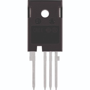
A Wolfspeed 650 V MOSFET.
These successes have provided the bedrock for much more progress over the past 25 years. During this time, SiC has gained commercial momentum that continues to accelerate to this day. We are now in the midst of one of the largest potential transformations in the entire semiconductor industry since the shift in silicon technology from bipolar to CMOS in the 1980s.
Mainstream breakthrough
One of our big, early successes came in 1996, when our blue LEDs were designed into the dashboard of Volkswagen vehicles. Prior to that, we had been selling less-efficient SiC LEDs, but in 1995 we introduced successors based on GaN-on-SiC. Our win with Volkswagen provided the first large-scale use of GaN-on-SiC LEDs in vehicles and signalled an acceptance of this technology – it had matured to a point where it could be adopted by a mainstream automotive player. Key to this acceptance, starting back then and maintained today, is the supply of SiC material. In the early 1990s it was extremely difficult to efficiently and effectively grow SiC crystals, which provide the foundation for LEDs and other devices.
Part of the reason why it is so challenging to produce high-quality SiC substrates is that there are more than 200 different crystal structures associated with various polytypes, and only a few are suitable for the semiconductor market. Adding to the complications, crystal growth requires temperatures nearing 2,500 °C. It’s hard to have a feel for such a high temperature, but to put it in perspective, it is half the temperature of the sun and significantly beyond that of molten lava, which is in the range of 1,700 °C.
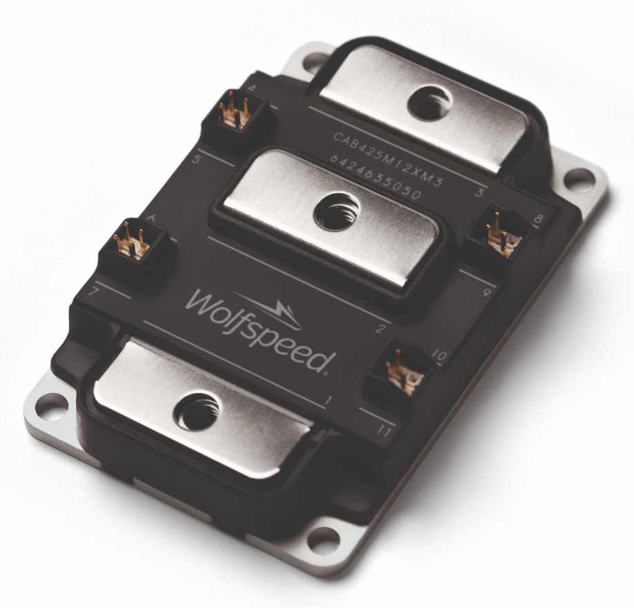
Wolfspeed’s XM3 style SiC Power Module.
Sustaining the needs of a major auto manufacturer drove our first breakthrough in our production of SiC. And this is still a topic of conversation in today’s market, where makers of automobiles are integrating SiC in far higher volumes into the drivetrain and chargers of mass-market, battery electric vehicles.
A lighting revolution
Following that first large-scale automotive use of LEDs, the world experienced a meteoric rise in cell phones. Previously a luxurious, somewhat novelty item for the well-to-do, it quickly became a must-have device for many. Since then, handset makers have been churning out millions of units every year.
When the market ramped in 2001, manufacturers of mobile devices started to incorporate LEDs into their latest models. Initially they backlit keypads, and a few years on, they were the light source for colour screens. They are ideal for that task, due to their low energy consumption, small footprint, robustness, and capability to be driven by a battery. The substantial volume of LEDs produced for this market spawned another huge leap forward for GaN-on-SiC sales.
GaN-based LEDs had now found their first killer application. However, although they had made much progress, they still had a long way to go before they could be viewed as a viable candidate for everyday lighting. Before that could happen, there needed to be an expansion in the colour palette generated by these sources, a hike in their efficiency, and a drop in price so they could be a competitive rival to the incandescent bulb.
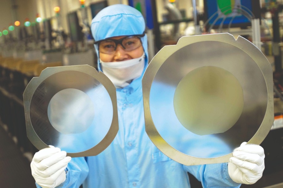
A Cree employee demonstrating the move from 100 mm to 150 mm SiC substrates.
Cree made much progress on all these fronts, introducing, in 2006, the industry’s first lighting-class LEDs. Known as the XLamp portfolio, these devices delivered 100 lumens per watt, exceeding the efficiency of fluorescent lighting. A revolution in lighting had started, after decades witnessing relatively little change.
LED lighting has many virtues. It’s robust, long-lasting, free from mercury, and its great efficiency trims electricity bills, in turn helping to reduce carbon footprints. But initially it did not find favour with the existing lighting infrastructure sector. That’s not that surprising, given the great business model of selling products to the public that could often fail within a year and had to be replaced. To drive a transformation, we started selling our own LED lighting fixtures to show the world what is possible. Our products consisted of a wide variety of indoor and outdoor lighting fixtures, ranging from fluorescent fixture replacements to LED streetlights.
Our final demonstration came in 2013, when we released our first LED light bulb. Rather than looking like something emerging from a science project, it had the style and feel of an incandescent bulb, and it retailed for less than $10. Launched to initiate the mass adoption of LED lighting, we called it ‘the biggest thing since the lightbulb.’
Following those major breakthroughs in LED lighting, we began putting additional emphasis in innovations outside the lighting space. This set us on a course for where we are today. Now our focus is to become a global semiconductor powerhouse that leads the transition from silicon to SiC.
Taking on the RF world
In 1998, we had our first major breakthrough in the RF domain, demonstrating the first GaN-on-SiC HEMT. Compared with the GaN-on-sapphire variants of the time, this device delivered increased signal gain and a 400 percent hike in power density in terms of watts per mm, making it an attractive candidate for wireless and broadcast high-power applications.

Cree employees examine product wafers.
Further success came in 2008, when we introduced the first GaN RF device that utilised the benefits of GaN-on-SiC to improve RF performance. With its high breakdown field, GaN can operate at very high voltages, and thus high-power densities, without having to compromise reliability. By using SiC as the foundation, the GaN device sits on a very high-thermal-conductivity platform. This base is ideal for dissipating a high-power density and maintaining junction temperatures at a reasonable level. Thanks to this, GaN RF devices deliver higher output powers without having to increase device size. These attributes enable the RF industry to design smaller, more efficient, more powerful RF systems.
During the last decade, we have continued to advance the performance of our RF GaN-on-SiC devices. They are widely adopted by the aerospace and defence industries, which use them to improve the capabilities of their systems as well as in the telecom infrastructure market for higher-efficiency power amplifiers.
SiC powers up
Power electronics started coming of age at the beginning of the twentieth century. One of the earliest examples is the mercury-arc rectifier, developed in 1902 to convert AC power into a DC form. By the early 1930s, selenium had replaced mercury, only to be superseded by silicon in the 1950s. During that era engineers invented the first silicon BJTs and MOSFETs, but the latter would not become suitable for use in power electronics until the late 1970s. The last major breakthrough in silicon power electronics, the development of the IGBT, followed in the 1980s.
Within the power electronics world, the introduction of SiC provided the next big materials breakthrough. The US Army, Air Force, Navy, NASA and DARPA all supported these efforts, funding programs from the early 1990s. For SiC to establish itself as a mainstream technology, SiC wafers had to be cheaper, larger, and contain far fewer defects. Without a substantial fall in defect density, it would not be possible to produce devices with sufficient area to operate at high currents.
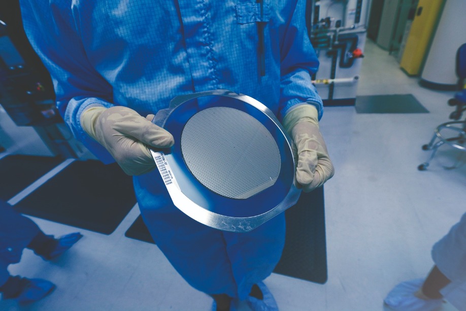
A up-close look at a 150 mm wafer in dicing.
A major impediment was the infamous micropipe defect. At one stage it was thought that micropipes were simply inherent to SiC, so impossible to eliminate. And that was not the only major stumbling block – oxides on SiC were considered to be inherently unreliable, preventing the manufacture of a reliable MOSFET. Even if both these daunting issues could be overcome, maybe that would be to no avail, if SiC wafers were never big enough to allow devices to serve in anything other than the most niche, cost-insensitive applications.
As history attests, all these issues have been addressed. Success on all fronts occurred after the launch of the first small SiC Schottky barrier diodes – introduced in 2001 and 2002 by Infineon and Cree, respectively – with progress paving the way to the introduction of first commercial SiC power MOSFET, which we launched in early 2011.
The introduction of SiC diodes and transistors has had a significant impact on the power electronics industry. It opened the door to faster switching frequencies, higher efficiencies, and superior power densities – all of which are key to the continued development of effective power electronic systems. These attributes allow SiC power electronics to support various emerging industries, including: renewable power conversion, such as solar energy and wind power; energy storage conversion; and electric trains, buses, and other types of public transportation.
SiC power devices can also be found in uninterruptible power supplies, industrial high-frequency power supplies, and motor drives. In all these applications, systems sporting SiC components operate with higher efficiencies take up less space, weigh less, and do not require extensive cooling systems. These valuable merits have taken us to a point where SiC is pushing the boundaries of innovation in a wide variety of industries.
An attitude of innovation
When we look back at these milestones over the past 25 years and think about all the breakthroughs in between, it is clear that Cree’s stubborn pursuit of innovation has been a driving force, both through the company’s history and that of SiC. There have been many obstacles, some considered insurmountable. It has led some to try and then give up, and others to never embark on these challenges.
There were those who argued that you cannot eliminate micropipes in SiC, that you can’t make a wafer larger than two inches, and that it’s impossible to make bipolar devices that don’t degrade. Cree has proved all those fallacies wrong due to a steadfast commitment to overcoming barriers. It is in our DNA that there is no reason to give up, just because someone says it can’t be done.
In some cases, we have not just broken barriers – we have kept on going, setting new benchmarks. After making the first 2 inch SiC substrate, we broke the 4-inch barrier, and now we’re ramping up 200 mm wafers, with mass production slated for the not too distant future. While it has certainly been a challenge and adventure to get this far, there is still so much more to come. As we look ahead, we see a future that has never been brighter. SiC is set to play an ever greater role in a variety of applications.
One of the biggest opportunities for SiC is in electric vehicles. Some of the first cars utilising this material are already on the road, and virtually every global manufacturer is including this technology in future designs that will grace the forecourts in the coming years. By replacing silicon devices with those made from SiC, the range of an electric vehicle can be extended by 5-10 percent, or the cost expended on expensive batteries trimmed by this amount. This most-welcome advantage is quickly positioning SiC as a necessary component in inverters as well as onboard and offboard chargers. As range is a significant factor for those considering the purchase of an electric vehicle, it has a tremendous influence on sales. And the use of SiC doesn’t always command a premium for electric-vehicle makers, as it can lead to an overall decrease in cost compared with the use of silicon technology. Its role looks set to grow further as electric vehicle manufacturers transition from 400 V to 800 V systems, which get an even bigger benefit from the switch to SiC, in terms of efficiency and other measures of performance.

Throughout the last 25 years there has been rapid innovation within the communications sector. It is currently undergoing a proliferation of 5G networks and picocells as well as higher volumes of small distributed antennas, radar applications, aerospace and defence tools. For all these applications,
GaN-on-SiC devices have the edge over silicon in efficiency and bandwidth, while offering a far smaller footprint. Drawing on the advances wrought by SiC has increased demand for this material. To bolster global supply, of which we account for 60 percent, we have committed to a $1 billion expansion at our Durham headquarters as well as the construction of an additional manufacturing facility in the Mohawk Valley, New York. When this additional production is available, our company’s capacity will have increased 30-fold from its level in 2017.
In the past 25 years, there has been more change in the SiC and semiconductor industries than we could ever have imagined. Looking ahead, the next 25 years are shaping up to be even more transformational. We expect that they will deliver breakthroughs that seem impossible today. It is an exciting time to participate in these changes, while looking forward to ground-breaking times that lie ahead.
Exposing indium clustering
How can GaN LEDs be so efficient, despite being riddled with defects? One potential answer, attracting much attention in the device’s early days, is that defect-free indium clusters in the InGaN quantum wells localise carriers and ensure efficient recombination. But subsequent work by Sir Colin Humphreys’ team at the University of Cambridge poured cold water on this idea, indicating that clustering was a measurement artefact, caused by the electron beam. Irrefutable proof followed in 2011, when researchers at Cambridge and Oxford studied two samples with InGaN quantum wells, with one previously irradiated with an electron beam. Using an atom probe, this partnership found that the exposed sample had compositional inhomogeneities in its indium content. In comparison, the control sample had a naturally occurring, random distribution of indium atoms.
S. Bennett et al. Appl. Phys. Lett 99 021906 (2011)
PRINTING CHIPLETS
Several situations require moving thousands of chips from their original wafer to another platform. This takes place when producing displays from red, green and blue microLEDs, and creating concentrating photovoltaic modules equipped with tiny, multi-junction cells. Assisting with this task is the inventor of a powerful technique for massive parallel transfer of various devices, John Rogers from the University of Illinois, Urbana-Champaign. He and his co-workers pioneered using rubber stamps to pick up an array of chiplets and deposit them on another substrate. Their first demonstration began by producing single-wall nanotubes, GaN nanobars and silicon wires on separate substrates. Printing these components on a sheet of polyimide created circuits with a bottom layer of GaN HEMTs, followed by single-wall nanotube thin-film transistors and silicon MOSFETs.
J. Rogers et al. Science 314 1754 (2006)
BACK BARRIER ENHANCES THE HEMT
When GaN HEMTs are produced on silicon substrates, the standard architecture includes a GaN back barrier. But an AlGaN back barrier is better, according to work reported in 2011 by Farid Medjdoub and co-workers at the Institute of Electronics, Microelectronics, and Nanotechnology in Villeneuve d’Ascq, France. Their devices, sporting an Al0.08Ga0.92N back barrier and a 6 nm-thick AlN barrier, alongside a 0.2 μm gate length and a 1μm separation between the gate and drain, produced a cut-off frequency in excess of 50 GHz – that’s twice that of a standard nitride HEMT. What’s more, the blocking voltage of the device is higher. Drawing on these benefits is not easy, because it is challenging to grow a high-quality AlN barrier. To prevent strain relaxation of AlN, the team coated this layer in a 3 nm-thick SiN cap, grown in situ.
F. Medjdoub et al. Appl. Phys Express 4 1241010 (2011)
BOOSTING BLOCKING VOLTAGES
When Infineon brought the first SiC Schottky barrier diodes to market in 2001, its pair of offerings could block 300 V and 600 V. The market welcomed these devices, but wanted to see even higher voltages, a feat that could be accomplished given that SiC Schottky barrier diodes had been shown to be capable of blocking 1 kV back in 1994. Those devices, using a palladium metal contact, featured nitrogen-doped, 10 μm-thick layers of 6H-SiC. In the years that followed, 4H-SiC had become available, increasing electron mobility; and researchers had switched to nickel and platinum contacts to realise higher blocking voltages. Drawing on both those advances, in 2003 a partnership between researchers at Rutgers University and Unite Silicon Carbide broke new ground, fabricating the first SiC Schottky barrier diode that broke the 10 kV barrier.
C. F. Huang et al. IEEE Electron Device Lett. 24 396 (2003)
DILUTE NITRIDES REACH THE C-BAND
What’s the ideal source for serving local and metro networks? It would have to be a VCSEL, because this device combines very fast switching speeds and on-wafer testing. And it would have to be built on GaAs, rather than InP, as substrates are lower in cost and larger in diameter. So the ideal device must be the dilute nitride VCSEL, a device debuted by James Harris’ group at Stanford University in 2006. Their first variant that reached the C-band contained three, 7.5 nm-thick Ga0.62In0.38N0.03As0.94Sb0.03 quantum wells, and produced a pulsed output at 1534 nm. By 2009, an improved design delivered room-temperature, continuous-wave emission in the C-band. The technology also found another outlet in the form of a university spin-off, Solar Junction. It pioneered record-breaking multi-junction cells with a dilute nitride bottom junction.
M. Witsey et al. Electron. Lett. 42 282 (2006)
ERADICATING ELECTRIC FIELDS
Conventional GaN lasers are hampered by the interplay of electrostatic forces and internal stresses that pull electrons in one direction and holes in another, hindering radiative recombination. But this issue can be avoided by turning to new planes for the growth of GaN. Switching to semi-polar planes reduces these fields, and they are eliminated with non-polar planes. Pioneering the later, a team at the University of California, Santa Barbara (USCB), announced the world’s first non-polar GaN laser in a press release on 29 January, 2007. Their bragging rights didn’t last long. Three days later Rohm revealed that they too had built a non-polar laser – and one with better performance. While the blue-violet laser from UCSB operated in pulsed mode, that from Rohm could produce a continuous output.
K. Okamoto et al. Jpn. J. Appl. Phys. 46 L187 (2007 )
M. C. Schmidt et al. Jpn. J. Appl. Phys. 46 L190 (2007)
WINNING THE GREEN RACE
To participate in the race to make the first green laser, you want access to GaN substrates. That puts those making them at an advantage. Exploiting that to the full came Sumitomo, smashing the record for a long-wavelength nitride laser in the summer of 2009. Until then, teams had built devices on conventional planes or non-polar variants. Sumitomo took a different tack, sporting a semi-polar variant that trims internal electric fields while aiding incorporation of indium in the InGaN wells. First-generation lasers included those producing emission at 531 nm when operated with a 0.5 percent duty cycle. After reporting these results in the August 2009 edition of Applied Physics Express, the team switched from a gain-guided to ridge waveguide design, and a month later reported a 520 nm device with a 2.5 mW continuous-mode output.
Y. Enya et al. Appl. Phys Express 2 082101 (2009)
Y. Yoshizumi et al. Appl. Phys Express 2 092101 (2009)
GETTING GALLIUM NITRIDE TO THE RED
When LEDs are used to form high-quality white-light sources through colour mixing, and create the red, green and blue pixels that make up a display, the production process would ideally involve just a single material system. The arsenide family is not an option, because as emission shortens, the bandgap switches from direct to indirect. That makes the only real contender InGaN. While external quantum efficiency in the blue can exceed 80 percent, in the green it is around 50 percent, and for longer wavelengths it is far, far lower. However, there is steady improvement in the orange, yellow and red, with a key milestone reached in 2014, thanks to research at Toshiba. Using an AlGaN interlayer in the active region to reduce the density of energy-sapping defects in the indium-rich quantum wells, this team produced a 629 nm device that broke the 1 mW barrier for a 20 mA drive current.
J-I. Hwang et al. Appl. Phys Express 7 0781003 (2014)
BLUE LASER BREAKTHROUGH
Wavelength limits data storage capacity. CDs, read by 780 nm lasers, hold just 780 MB, while DVDs, using shorter-wavelength 650 nm lasers, house up to 4.7 GB. Back in the late 1990s when CD players were in their heyday and DVD players started to appear, every maker of consumer electronics and PCs considered the possibilities of an even shorter wavelength laser chip. And it wouldn’t be long before they could get their hands on such a device, because by then Shuji Nakamura, Nichia’s star, had already laid the groundwork. News of the first GaN laser broke on 12 December, 1995, with details emerging shortly after. Nakamura’s laser emitted at 417 nm, not far from the 405 nm used for Blu-Ray players. His device, providing the shortest emission wavelength for laser diodes made from any material system, started to lase at 1.7 A and produced 215 mW of power at a 2.3 A drive current.
S. Nakamura et al. Jpn. J. Appl. Phys. 35 L74 (1996)
ROOM-TEMPERATURE LASING
Options for a narrow-emission source emitting at 2 mm and beyond include IV-VI ‘lead salt’ lasers, antimonide interband lasers, type II quantum well lasers and quantum cascade lasers (QCLs). All four are candidates for the likes of gas detection, infrared spectroscopy and laser surgery, but the QCL is the best option. Thanks to a unique emission process associated with intraband transitions, its performance is not held back by Auger recombination. That’s a massive asset, because Auger recombination is a major contributor to loss in the infrared. Early QCLs struggled to fulfil their potential, requiring cryogenic cooling to ensure lasing. But a team from Bell Labs lifted this restriction in 1996 with a GaInAs/AlInAs device producing lasing at 5 μm at temperatures of more than 45 °C when driven in pulsed mode. Peak power hit 200 mW.
J. Faist et al. Appl. Phys. Lett 68 3680 (1996)
During the last 20 years deep-UV LEDs have been invented, improved, and commercialised, allowing them to replace mercury lamps in disinfection, polymer curing and skin treatment products
BY Asif Khan FROM THE University of South Carolina
The 1990s will be remembered for the birth of efficient blue and green LEDs based on GaN. In the decade that followed, further improvements came that you literally can’t see. This triumph resulted from extending the emission wavelength of GaN LEDs into the ultraviolet. Replacing the InxGa1-xN quantum wells with those made from AlxGa1-xN allowed devices to reach the ultraviolet realm, emitting in regions known as the UVB (315 nm to 280 nm) and the UVC (280 nm to 100 nm).
Further progress has followed, and today several companies from around the world are pursuing large-scale manufacturing and commercialisation of these solid-state sources, which are being deployed in many applications. Here, we provide an overview of this progress, including details of the accomplishments of several groups making major contributions. We begin with a historical perspective, before providing an account of the current-status, the emerging applications, and finally some of the latest research directions.
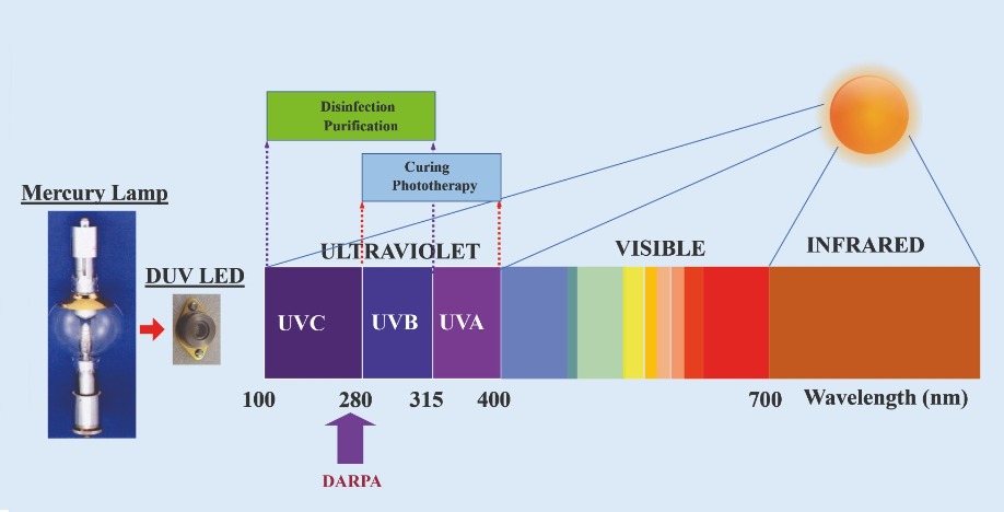
Figure 1: Solar spectrum and important application areas for UV LEDs. Shown is the wavelength requirements for the various application systems.
Major milestones
Two trailblazers of the UV LED are our team from the University of South Carolina, and the group at NTT, Japan. At the beginning of 2001 NTT reported a device emitting at 346 nm, and shortly after we unveiled an LED with a peak output at 341 nm. These two devices broke new ground, featuring the first active regions made from the pairing of AlGaN and AlInGaN layers. Before the year was out, we had made further progress, realising 315 nm emission, the edge of the UVB domain. And a year later, we eclipsed that success, reporting an LED with a milliwatt output power, emitting at 278 nm, just inside the UVC band.

Figure 2: (a) Device epilayer structures for the first-generation devices. (b) Epilayer design for second-generation devices that produce 1 mW, and have an external quantum efficiency (EQE) of 1 percent. The arrows (1 through 4) depict the key design changes that led to the higher power and EQE values. (c) Device configuration with flip-chip geometry. (d) Transmission electron microscopy of the nested short period superlattices used in the formation of strain/defect mitigation AlN/AlGaN superlattices.
Like many first-generation LEDs, these devices had a very low external quantum efficiency. Four factors were to blame: extended defects, resulting from lattice-mismatched growth of AlN/AlGaN layers on sapphire; a low doping efficiency, prevalent in p-AlGaN layers; the absorption of many of the photons exiting the quantum wells by hole-supplying p+-GaN; and a low light-extraction efficiency, exacerbated at the very shortest wavelengths.
By tackling these issues, the developers of UV LEDs made much progress over the next two years. For our team, as well as several other US institutions, efforts were supported by DARPA and the US Army. These bodies funded the SUVOS programme, managed by Lt. Col John Carrano. During SUVOS, we improved our materials, their growth, and the design and packaging of our device. These modifications created devices with an external quantum efficiency around 1 percent and an output power of nearly 1 mW at a 25 mA drive current.
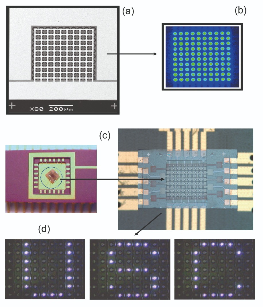
Figure 3: A 10 x 10 array micropixel LED that emits at 280 nm. (a) a scanning electron microscopy image of a 280 nm deep-UV LED with a 10 x 10 micropixel array. Each pixel diameter is approximately 30 μm. (b) the image of the micropixel LED under bias showing a uniform emission. (c) a fully packaged device mounted on a dual in-line package, along with a zoomed-in device image, clearly showing the electrode geometry for the matrix addressing of the deep-UV LED pixels. (d) with a controlled biasing, the 7 x 9 pattern micropixel LED can be used for a UVC display, in UVC communication systems and for deep-UV photolithography systems.
Better performance resulted from a combination of: high-temperature, migration-enhanced pulsed epitaxy for the growth of AlN buffer layers, which have a thickness in excess of 2 μm; the introduction of a nested superlattice for the AlGaN layers of the AlN/AlGaN superlattices; inclusion of a magnesium-doped, electron-blocking AlGaN layer; incorporation of polarization-doped, graded-composition p-AlGaN layers (see Figures 2 (a) and 2 (b)); and flip-chip mounting of the devices on metallic carriers (see Figure 2 (c)).
As just mentioned, one of the features of our second-generation devices is an improved superlattice design that aids defect and strain management and boosts output power (Figure 2 (d)). In this refined architecture, the AlN/AlxGa1-xN superlattices are nested short-period superlattices. They are formed using an aluminium-composition of the AlxGa1-xN layer of the macro-superlattice that is a thickness-averaged composition of the nested short-period AlxGa1-xN/AlyGa1-yN superlattices. By adopting this approach, we could grow crack-free, high-quality n+-AlxGa1-xN (n-contact layers) with thicknesses well over 2 μm. Incorporating this layer into our LEDs increased current spreading, mitigated current crowding and increased the current at which power-saturation kicked in. Thermal management also improved, leading to a longer device lifetime.
Substantial progress followed. By 2005, we were able to report the stability of our devices and their suitability for bio-chemical detection. Our demonstration of high-power, stable UVC LEDs provided a tremendous foundation for their commercialisation in applications that included air and water purification. While these devices are now well off the pace, the level of performance they provided is very effective in killing viruses and bacteria such as Ecoli.
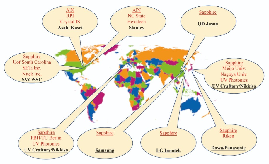
Figure 4: Global Partnerships for deep-UV LED development. Also shown is the substrate material that each team uses.
In addition to making significant contributions to the development of conventional, large-area UVC LEDs, we have also demonstrated a micropixel device. This configuration, reported in 2004, aids thermal management. Devices run cooler due to a reduction in total device resistance, a measure that combats current crowding and joule heating. Another merit of the micropixel device is that it allows biasing of individual pixels, making it ideal for deep-UV LED displays, UVC optical communication and deep UV lithography systems (see Figure 3). For the growth of UV LEDs, the most common substrate is sapphire. This material is transparent, low in cost, widely availability, and when used in combination with AlN buffer layers, it provides a good foundation for UV emitters. However, two US groups that manufacture bulk AlN substrates – Crystal IS and Hexatech Inc – have explored the potential of this platform for deep-UV LEDs. Note that other groups have not participated in this evaluation, due to the high cost and limited availability of AlN substrates. Although the use of native AlN has promise, one issue with bulk material is that during its growth, impurities are incorporated that have strong absorption in the UVC band.
Commercial conquests
Within the deep-UV LED community, university research groups have driven development. Their knowledge has transferred to start-ups, driving early commercialisation. More recently, several start-ups have formed partnerships, or been acquired by large companies.
Our team started this trend. Our deep-UV LED technology has been behind the launch of SETi and Nitek Inc, two small businesses in Columbia, South Carolina, that have been bought by Seoul Viosys Company and Seoul Semiconductors, respectively. In a similar vein, the technology from Nagoya University and Meijo University spawned UV Craftory Company, a start-up subsequently acquired by Nikkiso/FPG. Meanwhile, Riken’s technology has been directly acquired by DOWA/Panasonic; and more recently, in Germany, the technology from TU Berlin/FBH has been transferred to UV Photonics.
It’s a similar state of affairs for deep-UV LEDs developed on substrates made of AlN. Technology invented at Rensselaer Polytechnic Institute underpinned the launch of Crystal IS, which has been acquired by Asahi Kasei. Likewise, research at NC-State created Hexatech, now part of Stanley. In addition, large corporations, such as Samsung, LG Innotek, QD Jason and Nichia Corporation, have also started to venture into the deep UV.

Figure 5: Different packaging schemes employed for deep-UV LEDs. Shown are (a) various TO-headers; (b) custom aluminized headers for better light extraction; (c) LED chip on board (International Light Corporation (web-site)); and (d) packages with epoxy and quartz domes.
Many different approaches are adopted for forming relaxed, thick AlN buffers. Such buffers are highly desirable, because their lower threading dislocation density lowers the defects in the active region and increases the LED’s internal quantum efficiency.
We are growing these buffers by high-temperature pulsed epitaxy and hydride vapor phase epitaxy, while researchers at Riken are creating them by ammonia flow modulation epitaxy and a team at TU Berlin is producing them by migration-enhanced lateral epitaxial overgrowth and the use of ex situ high-temperature-annealed sputtered AlN.
Commercial progress with deep UV LEDs has led to the launch of devices emitting between 240 nm and 300 nm. Despite significant progress, the external quantum efficiency of these devices and their wall-plug efficiencies fall well short of the figures for their visible counterparts. While InGaN-based blue LEDs realise figures of around 80 percent for these measures of efficiency, values for deep UV LEDs emitting between 266 nm and 300 nm are typically just 5-6 percent.
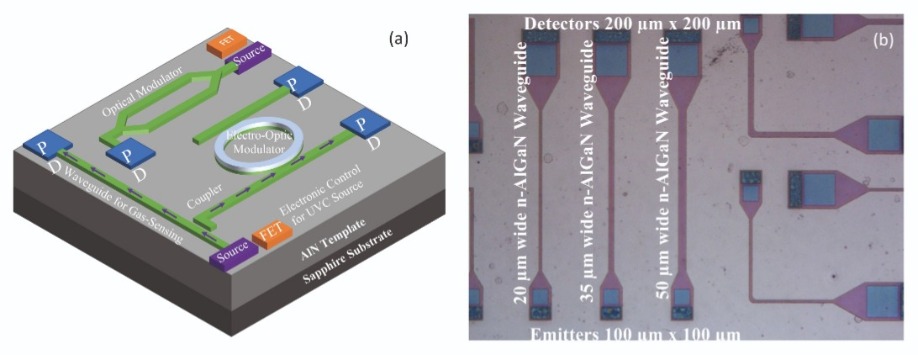
Figure 6: (a) schematic of a photonic integrated circuit (PIC) using the thick AlN on sapphire templates that are used for deep-UV LED epilayers. (b) A UVC PIC consisting of a UVC LED and UVC p-n junction detector connected using ridge waveguides.
As the emission wavelength shortens, the external quantum efficiency of deep-UV LEDs falls, along with its wall-plug efficiency. This is partly due to degradation of material quality, and difficulties in doping nitride-based alloys with increased aluminium composition. In addition, according to a team at Kansas State University, once emission drops below 270-280 nm, transverse magnetic-polarized emission becomes more dominant, due to a reordering of the valence bands. As this form of light travels lateral to the c-plane, it is efficiently trapped in the device, hampering photon extraction.
Today, there is a wide variation in the packages and form factors of commercial deep-UV LEDs. Discrete devices are available in TO-39 packages. This is not suitable for large devices, which require superior thermal management. These chips are housed in SMD packaging with AlN sub-mounts. Recently, there has also been the introduction of devices incorporating UV-transparent epoxy encapsulation (see Figure 5 for images of the different device packaging schemes).
For everyone working in the field of deep UV LEDs, the biggest challenge is to increase device performance to values comparable with visible counterparts. Today’s device design for commercial products has two major drawbacks. First, the p+-GaN hole injection layer leads to a loss of light travelling towards the p-contact and the wave-guided light in the active region. Second, light extraction efficiency is very low.
Approaches to mitigate light absorption by the p+-GaN layer and extract/collect more light travelling towards the p-electrode include the use of p-AlGaN layers. This approach has been pioneered by a partnership between Sensor Electronic Technology, Rensselear Polytechnic Institute and the US Army Research Laboratory; and also a Japanese collaboration led by RIKEN that has employed reflective p-contacts. Both teams have realised external quantum efficiencies as high as 10 percent.
Even greater success has come from RIKEN, working with Eco Solutions Company, part of Panasonic Corporation. They have reported external quantum efficiencies of 20 percent, realised by combining patterned-sapphire substrates and transparent p-AlGaN contact layers.
Future directions
It not surprising that by and large, the development of AlGaN-based deep UV LEDs is mirroring that of InGaN-based visible LEDs. The latter now incorporates tunnel junctions, a technology starting to be explored in deep-UV LEDs. By adding MBE-grown, UV-transparent AlGaN tunnel junctions contacts made from n++/p++-Al0.15Ga0.85N to MOCVD-grown active layers, researchers at The Ohio State University have doubled the output power and the external quantum efficiency of LEDs emitting in the 280-290 nm range.
Another area of research is deep ultraviolet integrated optics. Here, efforts involve integrating UVC optical and electronic components on a chip using UVC transparent waveguides made from AlN or aluminium-rich AlGaN. Our team, and a collaboration led by researchers at Nanjing University of Posts and Telecommunications, have provided initial demonstrations of the integration of UVC LEDs and detectors with planar and channel waveguides (see Figure 6 (a), detailing the device integration approach, and Figure 6 (b), an image of an integrated UVC LED/detector).
Successes like this have contributed to the tremendous development in deep-UV LEDs over the last 20 years. This device is already serving some applications, and as its robustness increases, along with its output power and its cost-competitiveness, its deployment will surge. The path that the deep-UV LED will take will essentially follow that of its blue predeccesor. It is traveling faster at some stages, taking just five years from the initial demonstration in 2002 to the first commercial products. However, another ten years elapsed for technology scale-up and power and efficiency improvements, all essential ingredients for the manufacture of low-cost devices delivering sufficient performance. Once new insights in the development of these devices are integrated into large-scale production, this should lead to a hike in the efficiency of commercially available deep-UV LEDs. We have come a long way in the last 20 years, and in the new two decades we should go far further.
APPLICATIONS of deep-UV LEDs can be grouped into disinfection, bio-medical instrumentation, polymer curing and bio-chemical sensing.
Due to the blocking of solar radiation in the UVC band by the earth’s ozone layer, most living organisms don’t have survival mechanisms to cope with the exposure of radiation in this spectral range. When organisms are exposed, changes to RNA/DNA take place, and impair reproduction.
Due to this, organisms become inactive. Note that different organisms require different dose levels, and to some extent, carefully selected wavelengths. When organisms are exposed to UVC LEDs producing an output of 100-125 mW and a peak wavelength of about 265 nm, a flux of 40-50 mJ.cm-2 results that can incapacitate most bacteria, spores, and viruses. Several UVC LED companies, or their strategic partners, now sell systems based on UVC LEDs for purification. They can be used for point-of-use water purification of moderate volumes of water.
More recently, companies have started to investigate the use of UVC radiation for surface decontamination of viruses, such as Covid-19. Taking the lead is the Seoul Viosys Company. Its Violeds deep-UV LED technology is being incorporated in the Fresh Air brand of air-conditioners, manufactured by ‘Gree Electric Appliance Inc’, the largest Chinese manufacturer of air conditioners. Another adopter of this type of technology is the RGF Environmental Group, a leading in-duct air treatment supplier in the US. Such efforts demonstrate that deep-UV LED technology provides protection against a variety of harmful organisms.
Another class of deep-UV LED applications is polymer curing. When UVA/B/C radiation reaches polymers, this initiates chemical reactions. What happens is that the exposure of photo-initiator molecules creates free radicals, which drive the polymerization of monomer and oligomer molecules. Curing applications are the backbone of key industries such as coatings, ink printing, adhesives, and photolithography.
Deep UV LEDs are also very effective at generating photochemical reactions in living organisms. LEDs that emit in the UVB are an excellent source for enhancing the concentration of metabolites. This means that plant growth cycles, flavour and quality can be controlled using deep-UV light exposure. As well as bringing an economic benefit, this allows these sources of UV light to have far reaching implications for fighting global food shortages.
Phototherapy systems provide yet another commercial opportunity for deep-UV LEDs. These systems are currently in use to treat vitamin D deficiency, seasonal effective disorder, and psoriasis.

A point-of-use water purification system (left). A list of viruses and bacteria that the air-conditioning systems with incorporated UVC LED array can mitigate (middle). A UVB LED based psoriasis treatment system (right).
Submilliwatt operation of AlGaN-based ultraviolet light-emitting diode using short-period alloy superlattice T. Nishida, H. Saito, and N. Kobayashi, Applied Physics Letters 78, Number 4, 22 January 2001
Ultraviolet light-emitting diodes at 340 nm using quaternary AlInGaN multiple quantum wells, V. Adivarahan, A. Chitnis, J. P. Zhang, M. Shatalov, J. W. Yang, G. Simin, and M. Asif Khan, Applied Physics Letters 79, Number 25, 17 December 2001
Milliwatt power deep ultraviolet light-emitting diodes over sapphire with emission at 278 nm, J. P. Zhang, A. Chitnis, V. Adivarahan, S. Wu, V. Mandavilli, R. Pachipulusu, M. Shatalov, G. Simin, J. W. Yang, and M. Asif Khan, Applied Physics Letters Volume 81, Number 26, 23 December 2002
Matrix Addressable Micro-Pixel 280 nm Deep UV Light-Emitting Diodes, Shuai Wu, Sameer Chhajed, Li Yan, Wenhong Sun, Maxim Shatalov, Vinod Adivarahan and M. Asif Khan, Japanese Journal of Applied Physics 45, No. 12, 2006, pp. L352.
A Review of AlGaN-Based Deep-Ultraviolet Light-Emitting Diodes on Sapphire, Yosuke Nagasawa and Akira Hirano, Appl. Sci. 2018, 8, 1264; doi:10.3390/app8081264 www.mdpi.com/journal/applsci
Deep-ultraviolet light-emitting diodes with external quantum efficiency higher than 20% at 275nm achieved by improving light-extraction efficiency, Takayoshi Takano, Takuya Mino, Jun Sakai, Norimichi Noguchi, Kenji Tsubaki, and Hideki Hirayama, Applied Physics Express 10 031002 (2017)
Photonics integrated circuits using AlxGa1-xN based UVC light-emitting diodes, photodetectors and waveguides, Floyd, R., Hussain, K., Mamun, A., Gaevski, M., Simin, G., Chandrashekhar, MVS. Khan, A., Appl. Phys. Express, 13 (2019), 022003. https://doi.org/10.7567/1882-0786/ab6410
A bug-beating diode, Asif Khan, Nature 441 18 May 2006.
UV Light Treatment for Psoriasis – A Psoriasis Phototherapy Guide, https://psoriasiszap.com/uv-light-treatment-for-psoriasis
The emergence and prospects of deep-ultraviolet light-emitting diode technologies, Michael Kneissl, Tae-Yeon Seong, Jung Han & Hiroshi Amano, Nature Photonics 13 pages 233–244 (2019)
AlGaN deep ultraviolet LEDs on bulk AlN substrates, Zaiyuan Ren, Q. Sun, S.-Y. Kwon, J. Han, K. Davitt, Y. K. Song, A. V. Nurmikko, W. Liu, J. Smart, and L. Schowalter, phys. stat. sol. (c) 4, No. 7, 2482–2485 (2007) / DOI 10.1002/pssc.200674758
It is staggering how much we have accomplished over the last 25 years. We have invented several devices and manufactured a variety of widely deployed, highly valued chip technologies. Our triumphs include: the development of blue and green GaN lasers, variants that emit from the surface of these chips, and a portfolio of gallium oxide power devices; the high-volume production of powerful LEDs that backlight screens and have revolutionised the light bulb; the commercialisation of SiC diodes and transistors that are driving increases in the efficiency of electrical circuits; and the construction of GaAs fabs that have churned out billions of amplifiers, a key ingredient in mobile phones. Read on to hear about all these successes and many more, as we take a look at the biggest story for every year, starting way back in 1995, when this magazine made its debut.
By summer 1995, Shuji Nakamura, trailblazer of efficient blue LEDs, had already become an industry celebrity. After inventing this device in 1993, he remained in the limelight by setting a series of ever higher benchmarks for the performance of this light-emitting chip. These successes enriched his standing within the tech pantheon of all-time greats and brought many accolades, including the biggest of all, a Nobel Prize for Physics, coming in 2014. But he got even greater pleasure from seeing his work laying a foundation for a lighting revolution.
While Nakamura is undoubtedly renowned for contributions to the development of the GaN LED, it is by no means the only ubiquitous device he has invented. He is also the originator of the cousin of the GaN LED, the GaN laser diode. The latter is an astonishing triumph. While many manufacturers are making millions of GaN LEDs every month, 25 years on from its introduction, there are still only two high-volume makers of the GaN laser diode: Nichia, where Nakamura worked throughout the 1990s; and Osram Opto Semiconductors of Regensburg, Germany.
Nakamura’s laser breakthrough came in late 1995, with news breaking on 12 December. Nichia’s greatest engineer appeared on TV later that month on a national evening news broadcast, demonstrating his wonderful new device.
By early 1996, details of the laser diode started to appear in the scientific press. A paper in the Japanese Journal of Applied Physics described a 30 μm-wide, 1500 μm-long stripe laser grown on a sapphire substrate. Emitting at 417 nm, it had an active region containing 26 quantum wells, each made from a 2.5 nm-thick layer of In0.2Ga0.8N. To get this device to lase, the voltage had to be cranked up to 34 V. Driven in pulsed mode at even higher voltages, this chip produced an output of more than 200 mW. Encouragingly, this laser showed no signs of degradation after two hours of operation.
Even before its debut, the entire optoelectronic industry had little doubt regarding the killer application for this short-wavelength laser diode. Back then most music lovers bought CDs, VHS recorders were on the verge of being replaced by DVD players, and even better picture quality was now on the horizon, thanks to a five-fold hike in storage density enabled by blue-violet lasers.
Those keen to splash out on a new generation of disc players that would allow them to watch high-definition movies in their own homes had a really tough time. Early adopters began by getting caught up in a format war between the advocates of HD DVD technology and those giving their backing to Blu-ray. When that had been resolved, allowing customers to pay top whack for one of the first Blu-ray players that hit the shelves in Japan in 2003, further frustration followed – those early adopters had to wait several years for the launch of the first titles.
Fortunately, some good years followed, providing a growing, lucrative market for the blue laser diode. Since then the increasing uptake of streaming services has sent sales of Blu-ray players into terminal decline – but as this door has shut, several others have opened. Blue lasers are now being deployed alongside red and green variants in colour projectors, and they are used also in copper welding systems, where they operate at an absorption sweet spot, enabling excellent welds. There is also the possibility that one day lasers will replace LEDs in general lighting – so maybe, just maybe, there will come a time when society is as thankful to Nakamura for his laser as they are for his LED.

Shuji Nakamura, inventor of efficient GaN LEDs and GaN lasers, sitting next to Nobuo Ogawa, founder of Nichia. Credit: Bob Johnstone.
Back in 1985 very few owned a mobile phone. Those that did included Karen Bertinger, the wife of a Motorola executive, who tried to reach her husband while holidaying in the Caribbean. Her call failed to get through, convincing the intended recipient, Barry Bertinger, of the need for a truly global wireless communication network. To build this, Motorola founded and financed Iridium, a spin out that would advance telephony through the launch of 66 satellites, all placed in low-earth orbits.
By 1996 makers of III-V photovoltaics were busy producing the devices for powering these satellites. Although silicon cells were still winning sales in the space sector, single-junction GaAs devices were in the ascendency. Despite costing five-to-eight times as much as their silicon siblings, they were favoured due to their higher efficiency. At the start of their life, they had an efficiency 25 percent higher – and crucially, at the end of life, after being battered by radiation, they were 40 to 60 percent more efficient. Given that each Iridium satellite required 24 m2 of GaAs cells, using these devices rather than those made from silicon led to a significant reduction in the solar-cell footprint.
Helping to fulfil orders for GaAs solar cells were a pair of Californian photovoltaic manufacturers: Spectrolab, at the time a subsidiary of Hughes and now part of Boeing; and Tecstar. For the latter, thanks to involvement in the Iridium project, production in 1996 totalled 200,000 3-inch wafers, equating to 140 kW of power.
Engineers produced these cells on germanium substrates. They were half the price of those made from GaAs, and much stronger. This use of germanium generated much business for the makers of the raw material – the price of high-purity polycrystalline germanium rocketed, climbing by a factor of seven in just 18 months – and ramped sales for two leading substrate makers, the US firm Eagle Pitcher and the Belgium outfit Union Minière, now known as Umicore. In 1996 germanium substrate consumption totalled between 300,000 and 500,000, with sizes ranging from 1.5 inch to 4 inch.
On 1 November, 1998, the Iridium network launched to much fanfare, with the first call placed between US Vice President Al Gore and Gilbert Grosvenor, great-grandson of Alexander Graham Bell.
However, despite this great publicity, the service never caught on. Potential customers balked at paying $2500 for the handset. Dropping this to $1495 and slashing service costs to two-thirds failed to turn the business around, and even by the end of 1999 Iridium had just 15,000 subscribers, a far cry from an anticipated 500,000. An inevitable filing for bankruptcy followed.
Failure of the venture took its toll on photovoltaic maker Tecstar. In 2001 it tried to branch out into LED epiwafers. Diversification did not go well, and in 2002 Tecstar’s management decided to call it a day, selling it solar division to Emcore for $21 million. Today, the technology is in the hands of SolAero, formed in late 2014 through the sale of Emcore’s solar power business.
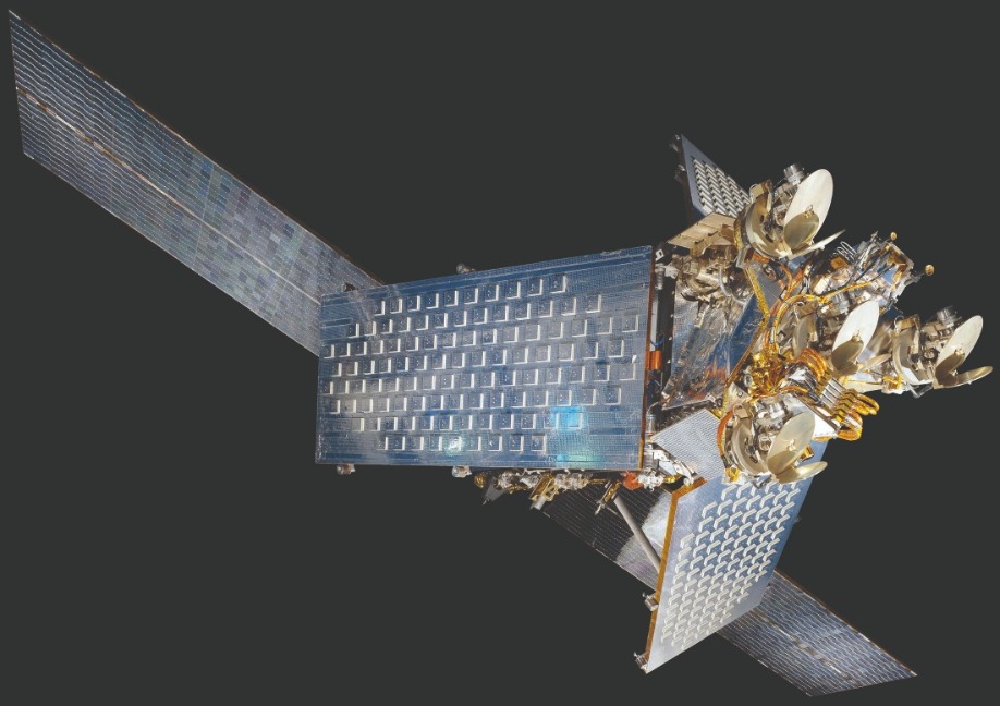
With 66 satellites each requiring 24 m2 of GaAs solar cells, the Iridium project, which aimed to provide global cellular coverage, generated much revenue for the III-V photovoltaics industry. Credit: Eric Long, National Air and Space Museum, Smithsonian Institution.
Owning a mobile may not have been the norm in the early 1990s, but it became increasingly common towards the turn of the millennium. The uptake of these handsets helped to swell the sales of makers of GaAs microelectronics, and provided the impetus for several of these firms to reach milestones, including three in 1997: the launch of RFMD on the stock market, the shipment of Rockwell’s two-millionth HBT, and Anadigics’ sale of its millionth GaAs IC.
RFMD, now part of Qorvo, started out as a fabless supplier of GaAs MESFETs, silicon bipolar devices, and HBTs, which provided 85 percent of sales. As demand for the latter ramped, RFMD couldn’t keep pace, losing a key contract with Qualcomm.
To prevent this from happening again, RFMD built its 4-inch GaAs fab in Greesnsboro, NC, in the late 1990s. Constructed in two phases, the facility initially produced 10,000 wafers per year, before eventually increasing to 25,000. Funding for this facility came from an IPO, supported by RFMD’s source of HBT wafers, TRW. It would become RFMD’s biggest shareholder, taking a 31.1 percent stake in the company.
For Rockwell Semiconductor Systems, the latter half of the 1990s will be remembered for an explosive ramp in the production of its HBTs, made in its 4-inch fab. During the 18 months spanning the beginning of 1996 to the middle of 1997, production at this company – which went on to form Skyworks Solutions in 2002 through a merger with Alpha Industries – mushroomed from just 10,000 units per month to 70 times that figure. Buyers of these HBTs included Qualcomm and Samsung. Both valued this class of transistor for its combination of excellent linearity and high efficiency, attributes ideal for making handsets based on CDMA technology that featured long talk times.
Rockwell faced competition for this business from Anadigics, which had shipped more than a million GaAs ICs supporting the CDMA standard by summer 1997. While most of Rockwell’s HBTs were being incorporated into phones operating in the 800 MHz to 900 MHz band, parts for Anadigics were providing amplification in transmitters of handsets using spectrum at 1900 MHz.
These higher-frequency products, based on Anadigics core technology, the MESFET, initially positioned the company for future success – but further ahead, contributed to its decline.
By the late 1990s, handset makers had shifted from using 6 V batteries to those providing 4.5 V and then just 3 V. This played into the hands of the increasingly price-competitive HBT. By the early 2000s, Anadigics ceased production of its MESFET, fighting back by developing a new generation of HBT.
Instead of having an AlGaAs emitter, it used InGaP. This refinement increased the HBT’s reliability, bolstered its high-temperature operation and improved its linearity. Anadigics’ product eventually proved a hit with handset makers, giving the company a healthy share of the 3G market.
When you think of high-volume manufacture of GaAs microelectronic devices, you’ll probably think of HBTs for smartphones. But that’s not the only market that has existed. In the telecommunications sector, a great deal of GaAs has been produced for laser and modulator drivers, multiplexers, demultiplexers, transimpedance amplifiers, clocks, and data-recovery circuits. In all these components, the higher speeds wrought by GaAs over silicon CMOS have yielded higher bit rates.
Back in 1998, when GaAs devices for the telecoms sector were flying off the shelves, Vitesse increased the production of products by building the world’s first 6-inch GaAs fab.
Unlike most construction projects, where deadlines come and go, Vitesse’s facility in Colorado Springs, CO, came in more than three months ahead of schedule. The first products, featuring GaAs MESFET technology, came off the line in early 1998, and in the third quarter of the year the company shipped $15 million of chips, based on 16 different products.
Vitesse, which also led the world in the migration from 3-inch to 4-inch GaAs production, built the 6-inch fab to cut the cost per die. Despite incurring a 25 percent hike in substrate-cost-per-unit-area, the switch to larger wafers delivered a 40 percent reduction at the die level.In the markets that Vitesse served, its technology had to continue to advance so that it could maintain a safe distance from products based on silicon CMOS.
The bursting of the dot.com bubble dealt a cruel blow, causing sales for Vitesse’s 40 Gbit/s devices to collapse and not recover before a 90 nm silicon process had caught up. This ultimately led to the closure of Vitesse’s GaAs fab in 2003.
After that, the company shifted focus, concentrating on silicon-based products for the metro, enterprise and storage market; and used its 4-inch InP fab to make high-speed electronic devices. The final chapter in the company’s history came in 2015, with its acquisition by Microsemi.
Even today, a 6-inch fab represents the state-of-the art for producing GaAs transistors. This might suggest that in the last two decades progress in chip manufacture has stalled. But consider this: in silicon CMOS fabs, the rapid advances in wafer sizes through the last three decades of the twentieth century have not continued into this millennium, and there may never be a 450 mm silicon fab.
For silicon, the 300 mm fab appears to be the sweet spot for production, with the investment required for any larger size failing to offer a suitable return – and for GaAs, the same could apply to the 6-inch line.
What makes for an ideal merger? In a nutshell, it occurs when the result is greater than the sum of its parts.
That appears to have taken place when Epitaxial Products International (EPI) joined forces with Quantum Epitaxial Design (QED) in 1999 to create IQE, the world’s largest epiwafer supplier. EPI of Bethlehem, PA, had built up its business by supplying MBE-grown wafers, used to make electronic devices, to a predominantly domestic market; while UK-based IQE had focused on optoelectronic epiwafers, with two-thirds of its sales coming from Europe and Asia.
The merged entity, offering a dual source of supply for some products, promised to be a resounding global success, drawing on the growing businesses of both companies. Sales at QED were increasing at a compound annual growth rate of 40 percent, while at IQE they were ramping at 30 percent. To cater for greater demand both sites had capacity expansion plans in place. QED had an order in for an MBE reactor capable of producing multiple 6-inch wafers from a single run, and EPI, which had recently increased the size of its facility, had placed orders for multi-wafer MOCVD tools. Helping to fund these expansion plans, IQE raised $70 million in an IPO, launching on the EASDAQ, the European version of NASDAQ, in summer 1999.
Since then IQE has strengthened its leading position in the epiwafer market. In 2006 it acquired the epi business of Emcore; the following year it bought MBE Technologies of Singapore; and in 2012 it acquired the epi-business of RFMD. It has also broadened its portfolio. The company added technology for realising high-quality GaN in 2009, by buying NanoGaN of Bath, UK; the purchase Galaxy Semiconductor of Spokane, WA, in 2010, equipped the multi-national with capability in antimony substrates and infrared technology; in 2012, the investment in Solar Junction strengthened expertise in multi-junction solar cells; and in 2018, the acquisition of Translucent’s technology brought on board capability in crystalline rare-earth oxides, enabling compound semiconductor films to be grown on silicon wafers. IQE is now a colossus in epiwafer manufacture and related technologies.
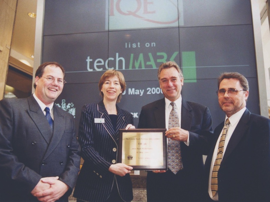
In 1999 the merger of UK-based Epitaxial Products International and US-based Quantum Epitaxial Design spawned IQE, which launched on the European equivalent of the NASDAQ.
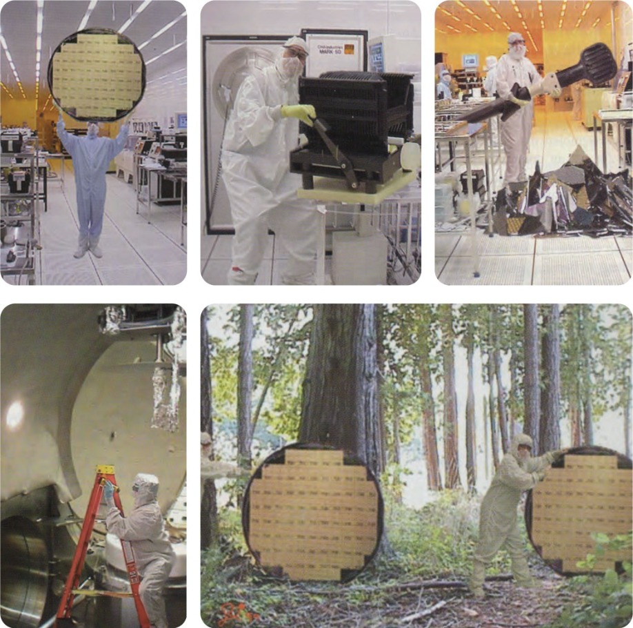
In the late 1990s and early 2000s GaAs fabs were transitioning to larger wafers. Injecting some humour into the race to gain bragging rights with ever larger lines, TriQuint provided ‘evidence’ of its 6-foot fab in a series of images, described in chronological order. (top left) TriQuint announced the start-up of the industry’s first 72-inch wafer assembly line by circulating a press release at the GaAs Mantech conference held in 1999. (top middle). TriQuint then revealed that some of its engineers had been working frantically to prevent heavy lifting. “Man these are some big GaAs-wafers,” commented one operator (top centre). In the next picture story (top right), a TriQuint technician remarked: “I don’t know what happened, it just fell off the wand!” TriQuint went on to explain how equipment maintenance can prove to be quite a chore in a 72-inch wafer fab. This equipment engineer is inspecting just one of the many massive vacuum chambers used in the evaporation process. (bottom left) In the final release (bottom right), TriQuint reported how excitement built at the 72-inch wafer plant as the first finished wafers were distributed through the ‘Silicon Forest’.
Internet traffic soared in the run up to the millennium, placing tremendous strain on optical communication infrastructure. Carriers addressed this by beefing up network capacity. This created an optical component sector worth almost $10 billion and tipped to increase at a compound annual growth rate of 40 percent. Makers of III-V optoelectronics were well-positioned to benefit from this ramp, as their devices accounted for up to half that market.
Understandably, frantic carriers did not want to deal with numerous component suppliers. They longed for one-stop shops, ideally offering modules that would drop into their networks.
To cater for this demand, acquisitions ran rife in the components sector. JDS Uniphase (JDSU), formed in June 1999 through the merger of the Canadian outfit JDS Optics and the US firm Uniphase, led this spending spree. In late 1999 JDSU signed a deal worth $400 million for photodetector maker Epitaxx, and in 2000 it made three monumental acquisitions: it snapped up Optical Coating Laboratory for $6.2 billion, E-Tek Dynamics for $15 billion and SDL Lasers for a whopping $41 billion.
Once the dot.com bubble had started to burst in the first few months in the new millennium, everyone knew the folly of buying a company for figure that is many times more than its annual revenue. That made the purchase of SDL, for which JDSU had forked out a sum equating to 142 times the annual revenue, an outrageous blunder. Hindsight exposed any notion of a new world order, rampant in the giddy highs, and traditional economics were back with a vengeance.
During 2000, inventory corrections kicked in within the supply chain, driving down margins. On 30 June of that year JDSU had the dubious distinction of reporting the biggest ever annual corporate loss – an eye-watering $ 56.1 billion (taking inflation into account, it’s now in fourth place, behind AOL Time Warner, American International Group and Fannie Mae). However, for JDSU this loss was predominantly on paper. The vast majority of the $56.1 billion came from a write down of goodwill associated with various acquisitions, which were primarily all-stock deals.
For investors, the downturn in company fortunes could not be dismissed so easily. In March 2000, spurred on by analyst claims that out-of-the-box visionaries were leading a great company in exactly the right place at the right time, shares in this Wall Street ‘darling’ peak at $1200. Go forward a few years and they had fallen by more than 99 percent.
The company’s leaders sold some of their shares near their peak, leading to accusations of fraud and insider trading. Some joked that JDSU now stood for Just Don’t Sue Us – and those representing the state of Connecticut did just that, hoping to recover losses from a pension fund. The case, filed in 2002, came to court five years on, with management cleared of fraud.
By then the company CEO of the glory days, Kevin Kalkhoven, had retired, using part of his wealth for philanthropic ventures. He also funded a car-racing team that notched up five victories, including the Indianapolis 500 in 2013.
As for JDSU, it no longer exists. The prolonged downturn in the optical component business took a heavy toll, with the company shedding 80 percent of its workforce and closing 29 sites. In August 2015 the company split, forming network test and measurement specialist, Viavi Solutions and the laser manufacturer Lumentum.

Kevin Kalkhoven, former JDSU CEO, co-founded PKV Racing, later known as KV Racing Technology. This team competed in both the Champ Car World Series and the IndyCar series, amassing five wins, including the 2013 Indianapolis 500.
What marked the beginning of the wide bandgap power electronic industry? It is surely Infineon’s launch of the SiC Schottky barrier diode, the first wide bandgap power electronic product to hit the market.
When this device made its debut in 2001 it filled a gap in the market. Silicon and GaAs Schottky barrier diodes were limited to blocking below 250 V to avoid very high leakage currents, exacerbated at high temperatures. Infineon’s pair of variants could handle 300 V and 600 V while carrying up to 1 A, and were far better at handling heat, giving them an edge for deployment in power supplies.
Infineon, which made these devices from 2-inch SiC wafers at its fab in Villach, Austria, targeted power supplies operating between 200 W and 1000 W. Used in that manner, the company’s diodes featured in servers and wireless base stations.
The designers willing to make the switch from silicon diodes to those made from SiC were well rewarded. Their supplies were more reliable and more efficient, and they could be smaller and lighter, as the SiC diodes allowed the operating frequency to increase, opening the door to a reduction in the size and weight of passive components.
Infineon’s first generation of SiC diodes sported a simple architecture, selected to try and minimise costs that were dominated by pricey 2-inch SiC substrates.
Since then substrates have increased in size and quality and fallen in price and diodes have been through several iterations, increasing in complexity. By 2018, Infineon had reached its sixth generation, a family of 650 V SiC Schottky barrier diodes capable of handling currents ranging from 4 A to 20 A.
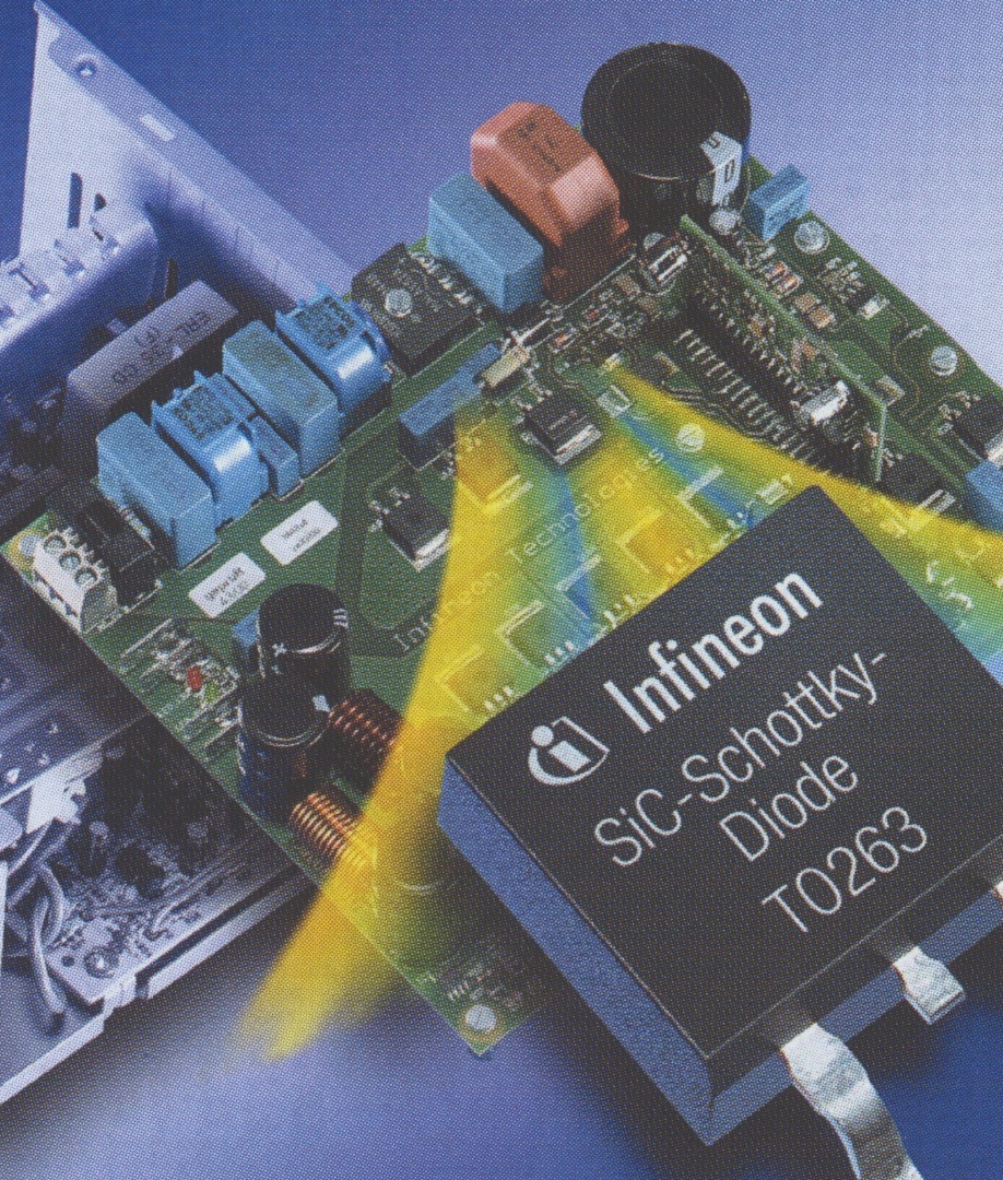
The birth of the wide bandgap industry came in 2001, with Infineon’s launch of the SiC Schottky barrier diode.
The compound semiconductor industry can never be accused of putting all of its eggs in one basket. But at the start of this century, it certainly placed two of its largest in there. Back then handsets provided the killer applications for: LEDs, used to backlight screens, illuminate keypads and provide camera flash; and GaAs transistors, used to amplify and switch
RF signals.
When the mobile phone industry was in its infancy, the focus would have been on attracting new customers. But within a few years efforts had broadened to include attempts to woo owners to upgrade their devices. In 2002, the cool new features were colour screens, built-in cameras, and picture and photo-messaging services.
In Japan, mobile network operator J-phone offered those that purchased a new handset the opportunity to send five second video clips accompanied by sound. Over the last two decades, the leading brands have changed markedly, shifting the fortunes of the makers of GaAs microelectronics.
In early 2002, when phones supporting 2.5G led the way, Nokia dominated the market with a share of more than 35 percent, providing GaAs-HBT manufacturer RFMD with about half its shipments.
Motorola occupied second spot with 16 percent of the market, followed by Samsung, Siemens, and Sony Ericsson. Fast forward to 2019 and Samsung had moved up to pole position, followed by Huawei, Apple, Xiamoi and then Oppo.
There has also been a substantial rise in annual phone sales. In 2002, this totalled just over 400 million, while last year almost a billion more were bought. A forecast made earlier this year suggests sales will fall by 200 million this year, due to the financial impact created by Covid-19.

The introduction of colour screens in handsets in the early years of this millennium helped swell sales of LEDs.
As we emerge from the pandemic, many are wondering what shape the economic recovery will take. We hanker for a “V” – that is, that after the sharp decline there will be an equally sharp rise that speeds us to a time of steady, sustained growth. Unfortunately, probably the best we can hope for will be a “U”, with a few tough quarters in store before we return to better days. What we are desperate to avoid is an “L”, a decline that leaves a permanent scar on the economy.
Sometimes some sectors will experience an “L”, even when the general economy is on the up. That happened to component makers within the telecommunications market in the ‘noughties’,
leading to a flurry of activity in 2003. When the dot.com bubble started to burst, the III-V chipmakers operating in this industry initially put the problem down to inventory corrections. However, by 2003, with orders still failing to pick up, it became clearer that the real issue was long term over-capacity. This cannot be fixed when facilities change hands – all that can do is potentially increase production efficiency. The hard reality is that when there are more fabs than needed to supply demand, some have to be closed and workers laid off.
This chain of events can be seen in the activity at Bookham. Shortly after the bubble burst, it picked up Nortel Networks optical components division and Marconi’s optical components business. In 2003, to try and streamline operations, it started relocating Nortel’s former InP chipmaking facility in Ottawa, Canada, to the ex-Marconi facility in Caswell, UK. In addition, it moved the semi-automated line for laser assembly and test from its site in Zurich, Switzerland, to its facility in Paignton, UK. At that site, used to assemble optical chips into packaged products, headcount had already plummeted from a heyday figure of 7000 to just 800.
When a sector is struggling and showing no signs of recovery, it’s a good idea to diversify into new markets. In late 2003 Bookham positioned itself to do just that, purchasing Ignis Optics, a maker of transceivers for datacom networks, and New Focus, a provider of photonics and microwave products for semiconductor, biotech, defence and research industries.
In 2003 another major shift in the optical components landscape came from Avanex’s acquisitions of divisions of Alcatel and Corning. The former calved off Alcatel Optronics, while the later parted company with its optical components’ plants in Milan, Italy, and its optical amplifier facility in Erwin, NY. Corning’s restructuring also involved the closure of its Lasertron pump laser facility, purchased in a $1.8 billion stock deal in November 1999.
Further changes within the components sector in 2003 included: ASIP, a maker of InP optoelectronic components, purchasing struggling rival ThreeFive Photonics; integration of the optical chip processing lines at NTT Electronics and Oki Electric, used for lasers, photodiodes and modulators; Ericsson’s exit from the optical component business through its sale of Ericsson Optoelectronics to Swedish start-up Northlight Optronics; and Agere’s decision to bid farewell to this sector by selling its West Coast optoelectronics business to Emcore for $25 million in cash.
Following a hive of activity in 2003, restructuring of this sector slowed down, but did not stop. In 2009 Avanex and Bookham merged to form Oclaro, which went on to sell its Zurich GaAs laser diode business in a cash deal worth $115 million to II-VI Incorporated in 2013. And then, in 2018, Lumentum bought Oclaro, to expand its portfolio of laser products.
While it’s easy to view 2003 as just a year of gloom and doom, take a careful look and you can also find a silver lining. Back then, some canny investors were willing to pump cash into this sector, enabling Infinera to raise a whopping $53 million in series D funding in the latter half of the year. This Californian-based outfit has blossomed, netting billions of dollars and making a strong case for the virtues of vertical integration in the telecom sector.
The handset provided the first killer application for the GaN LED. Used to illuminate keypads and backlight screens, manufacture of this device exploded as mobiles became a must-have accessory. This led the leading LED makers to face more competition. They knew that their margins in this market would slowly shrink, so they went in search of new, more demanding applications that would allow them to make more money.
The backlighting of far bigger screens offered a very promising opportunity, and in 2004 Nichia, Toyoda Gosei and Osram Opto Semiconductors all promoted LED-backlit screens at various shows. But rival Lumileds drew first blood, winning a supply contract to ship LEDs from its Luxeon range to Sony, for use in two of its flagship TVs for 2004: 40-inch and 46-inch Qualia models, retailing for around $7500 and $10,000, respectively.
Boasting a far wider colour gamut than screens incorporating cold-cathode fluorescent lamps, these TVs could not fail to impress. And there is no doubt that some early adopters would have been willing to pay a hefty premium to get their hands on this new technology. But the parting of their cash, which helped Sony to claw back some of its investment in R&D, did not lead to tumbling prices over the next few years, alongside a growth in shipments and major market success. Although that has happened for LED-backlit TVs, it has taken a relatively long time. Five years on from Sony’s launch, its high-end models were still retailing for thousands of dollars. By then TVs from Samsung, which also introduced LED-backlit TVs in 2004, were on offer for less, but they still had price tags of just under $2000 and $1500 for 46-inch and 40-inch TVs, respectively. It is only in the last decade that LED-backlighting has become more affordable, taken off and gone on to become the dominate technology.
As well as the start of LED-backlighting, 2004 will go down in history as the year that China started its quest to take a significant share of the market. The China National Solid-State Lighting Programme kicked off in June of that year, providing a tremendous level of support for home-grown chipmakers. This effort has ultimately been responsible for razor-thin margins in the LED industry, and the commoditisation of this device.

Samsung and Sony pioneered LED-backlit TVs. Launched in 2004 and costing many thousands of dollars, initial sales were sluggish. Thanks to a tremendous reduction in the cost of these screens, they are the incumbent technology today.
There’s an elegance in using a high-power laser to destroy tanks and missiles with a burst of incredibly powerful light. But even today, despite research and development into laser-based weapons going back 60 years, this idea is still a long way off becoming a mainstream military technology. There are various issues, including a phenomenon known as thermal blooming – it is a defocusing of the laser beam, caused by the creation of a plasma at very high levels of light intensity. Unfortunately, blooming is exacerbated by fog, smoke, dust and rain, none of which are strangers to the battlefield.
Despite all these concerns, in 2003 the US agency DARPA ran a three-year programme called SHEDS – super-high efficiency diodes sources – aimed at preparing the way for a laser-based weapon. This effort focused on propelling the wall-plug efficiency of commercial infrared laser bars from well below 50 percent to at least 80 percent. Hitting this target could lead to a highly-efficient 100 kW laser-based defence weapon, according to the sponsor.
Three US chipmakers took on the laser diode efficiency challenge: Alfalight, nLight and JDSU. All sailed past the 65 percent intermediate goal by refining their devices through initiatives that included the compositional grading of quantum-well interfaces, the introduction of materials that enhanced optical and electrical confinement, and changes to doping that cut contact resistance. But none could scale the dizzy heights to fulfil the final target, an efficiency of 80 percent.
Despite this failure, the programme has left a great legacy. And like many DARPA initiatives, the beneficiaries lie outside the military. Even in 2005, before the programme had finished, gains in laser efficiency were making an impact in industries that used solid-state, diode-pumped lasers for a wide variety of processing-related tasks, from shaping medical devices to welding car-body parts. Higher efficiencies were trimming the dollar-per-Watt metric, and in turn reducing expenditure on diodes that could total a third of the system cost. What’s more, device reliability improved, because greater efficiency meant less heat, and chips that run at lower temperatures.
Improvements to the diode’s bang-per-buck have also been instrumental in the success of fibre lasers. Offering a simple solution to the tricky problem of how best to focus light onto a target, diode-pumped fibre lasers are now widely deployed for cutting, welding, and folding of metals and polymers, with sales netting $3 billion per year.

Efforts to turn the vision of laser-based weapons into reality were supported by a DARPA-funded programme aimed at increasing the efficiency of infrared laser diodes from below 50 percent to 80 percent or more.
Silicon photonics sounds too great to be true. Whizzing photons around miniature racetracks in silicon chips churned out in state-of-the-art fabs promises a future offering affordable, breath-taking computational powers and superfast communication. But I know that you’ll have your doubts, because you know that silicon can’t emit light. That makes the manufacture of photonic chips quite a challenge.
If you want your light source on the chip, you’ll need to find a way to unite a III-V laser with a silicon waveguide while combatting problems arising from the significant lattice mismatch between these materials.
The first significant success in this endeavour came in 2006, through a partnership between engineers at Intel and John Bower’s group at the University of California, Santa Barbara. Using a low-temperature oxygen plasma, these researchers created a thin oxide layer on the surface of both materials. This layer enabled the fusing of an InP-based chip, containing AlGaInAs quantum wells, to the silicon waveguide strip, to create an electrically pumped laser. And due to the excellent coupling between these entities, the silicon waveguide played a fundamental role in the lasing action.
Building on this triumph, Intel had developed and commercialised a portfolio of transceiver products.
In 2016, it introduced a silicon photonics transceiver that supports 100G communications, and two years on, the company targeted 5G wireless front-haul applications with this product. This 100G transceiver has a transmitter and a receiver block, each with several die. The transmitter contains several InP lasers and a Mach-Zehnder modulator that encodes their signals, and the receiver features four germanium photodiode dies and a trans-impedance amplifier circuit.
Intel has now shipped more than 3 million 100G pluggable transceivers based on its silicon photonics platform, and demonstrated a four-channel device operating at 400 Gbit/s.

Intel has pioneered the integration of InP-lasers and silicon photonics. In this 50 Gbit/s link, the transmit module (left) sends laser light from the silicon chip at the centre of the green board, which travels through optical fibre to the receiver module (right), where a second silicon chip detects the data on the laser and coverts it back into an electrical signal.
Some scientific questions pique interest but actually don’t matter that much because they are only of academic interest. But in 2007, that was certainly not the case for droop. Back then this mysterious malady pegged back the efficiency of LEDs at the current densities needed to win business in the biggest market of all, general lighting.
At that point in time researchers had ruled out heating as the cause and dismissed indium clustering, attributed as a measurement artefact. The search continued, with much riding on success. Unmasking droop would offer insight into how to build efficient devices that could light our homes and offices.
In February Philips Lumileds came out with a stunning, bold claim, saying that it had ‘fundamentally solved’ the problem of droop. According to this Californian chipmaker, LEDs that were free from this malady would follow in a matter of months.
Rather tantalisingly, the company offered no details of the cause of this deficiency. But in September they spilt the beans at the biggest nitride conference of the year. At a buzzing International Conference on Nitride Semiconductors, held in the heart of Las Vegas, Mike Krames, at the time the leader of the company’s Advanced Laboratories, unveiled Auger recombination as the cause.
The claim drew a mixed reception. Partly, it is a cause no-one wanted, because it fails to offer a route to making droop-free devices. Auger recombination is an intrinsic process that depends on the carrier density, and all that can be done to reduce it is a form of social distancing at the atomic scale, such as a widening of the wells. But in practice it’s very difficult to produce thick, high-quality quantum wells, due to strain.
What’s more, not all researchers agreed with Krames and his co-workers.
Some questioned the magnitude of the Auger coefficient required for this to be the primary loss mechanism, while others argued that just because it’s possible to fit a curve to a graph with a cubed dependence classically associated with Auger recombination, that is not proof that Auger causes droop.
An alternative theory came from Fred Schubert’s group and Rensselaer Polytechnic Institute in Troy, NY, working in partnership with researchers at Samsung and Joachim Piprek, a theorist at the device simulation consultancy NUSOD. This team, which started publishing papers in late 2007, attributed droop to carrier leakage. They went on to build polarisation-matched devices delivering higher efficiencies at higher drive currents.
The debate on the cause of droop raged for many years. In 2013, as we shall soon see, independent work laid claims of a smoking gun, providing definitive proof that Auger recombination is the cause of droop. But even that did not convince everyone.
After many years of waiting, in 2008 the concentrating photovoltaic (CPV) industry looked like it would finally hit the big time. Venture capitalists had tired of investing in the telecommunication market and were starting to pour cash into cleantech, including developers of CPV, helping a handful of CPV companies to win contracts for multi-megawatt deployments. This led two makers of multi-junction cells – Spectrolab and Emcore – to fill up their order books. And competition for sales of these devices would soon increase, as the likes of Spire Semiconductors, MicroLink and Kopin prepared to launch rival products.
It had taken a long, long time for the fledgling CPV industry to get this far. The idea of focusing sunlight on highly efficient III-V cells can be traced back as far the late 1970s. A few years on from then a prototype had been put together by researchers at the Ioffe Physico-Technial Institute in St. Petersburg, Russia. Their system, reported in 1981 in a paper co-authored by Nobel-prize winning physicist Zhores Alferov, used reflectors as big as bin lids to direct sunlight onto 1.7 cm diameter AlGaAs/GaAs solar cells, butted up against aluminium pipes to prevent overheating. In the decades that followed, more demonstrators were put together, III-V cell efficiencies climbed and systems were built and sold, culminating in the deployment of a few tens of megawatts in the run up to 2008.
That year, market analyst Lux Research claimed that the long-term signs were great, with expenditure on installations employing III-V solar cells set to total $1.2 billion by 2012. Lux warned that some CPV start-ups would not survive, because they were failing to tackle important engineering issues surrounding maintenance, cooling and wind resistance. But that did not cause much alarm, as in an emerging market some firms will always go to the wall.
The unfortunate reality is that come 2012, the CPV industry was in tatters. Many firms had gone bust, while those that were left were on their last legs. The credit crunch, caused by a global economic crisis, starved these firms of investment crucial to increasing their size and delivering economies of scale. Another hammer-blow came from falling prices of silicon solar cells at the start of the last decade. Despite $500 million of investment, roughly just 100 MW of CPV has been deployed, with a lack of business bringing the demise of many big names in the sector, including Ammonix, SolFocus, Isofotón, GreenVolts and Semprius.
Today CPV is still down, but not quite out. In 2017, STACE, a supplier of electrical equipment in the power generation industry, bought the CPV assets of Soitec. Using this technology, which can be traced back to Concentrix, eight 30 kW CPV systems have been installed at the University of Sherbrooke, Quebec.
So, if further research into CPV allows it to become competitive enough to take on the incumbent – and that is definitely a big if – there is a company well-positioned to roll out this technology.

Interest in concentrating photovoltaics reached an all-time high in 2008. A leader in this field, Concentrix, used Fresnel lens to concentrate sunlight by a factor of typically 500 on triple-junction cells. A credit crunch and a dramatic reduction in the price of silicon PV wrought havoc in the fledgling CPV industry. Soitec purchased Concentrix in 2009, and then sold this technology to STACE, Canada, in 2015.
What is easier – using an efficient blue LED as a starting point to build a laser emitting in the same spectral range; or starting with a laser that emits in the blue-violet, and constructing a variant that emits in the green? You would think it would be the later. After all, to go from an LED to a laser you need to introduce optical confinement, create mirrors, crank up the local carrier concentration and slash the defect density in the active region. In comparison, to turn a blue-violet laser into a green one, all you need to do is add a little more indium into the quantum well.
But if you take a look in the history books, you’ll reach a very different conclusion. Courtesy of Shuji Nakamura’s pioneering work, Nichia reported the first efficient blue LED in 1993 and took just two years to follow it up with a laser. But nearly another 15 years elapsed before the world had made its first green GaN laser.
The first important step towards this source came in 2003, with Nichia’s report of a 480 nm laser – still blue, but leaning to the green. Five years on, it had only advanced another 8 nm. Had this device come up against an invisible wall, with blue-green being the limit?
Any chances of getting to true green, considered to be 520 nm and beyond, seemed to rely on a radical re-design. To reach longer wavelengths requires a cranking up of the indium content, realised by lowering the growth temperature in the MOCVD chamber. But this riddles the device with defects, degrading light emission. Compounding the problem, intrinsic electric fields in these heterostructures pull apart electrons and holes in the wells, and as the indium content increases, they get even stronger. While these fields are beneficial on one hand, pushing emission to longer wavelengths, they make it harder to inject carriers into the device. Turning up the voltage forces them through, but negates the benefit of the internal field, so it’s goodbye to longer wavelengths.
A novel way to overcome this issue is to switch growth planes. Growing the device on the non-polar plane quashes the electric field. In early 2007, a team at the University of California, Santa Barbara, that included Nakamura – he joined this group from Nichia in late 1999 – did just that. They unveiled the world’s first non-polar laser, emitting in pulse mode at 404 nm.
The joy of leading the way didn’t last long. Just three days later Rohm reported a non-polar laser, this time operating in continuous-wave mode. When Rohm reached this milestone, it also set out its true ambition: building a 532 nm laser for colour displays. Before the year was out, it had stretched emission to 459 nm. Although Rohm then lost the lead when Sharp entered the fray in 2008 with a 463 nm non-polar laser, it retaliated with a 481 nm device.
2009 proved a pivotal year. In February Rohm revealed yet more progress, reaching 499.8 nm and eclipsing the best mark for conventional nitride lasers. At that point, a non-polar laser would have been the bookies’ favourite in the race for the first GaN green laser. But anyone thinking along those lines got an almighty shock nine days later, when a conventional laser took the lead. This didn’t come out of the labs of Nichia, but from a very dark horse – Osram Opto Semiconductors of Regensburg, Germany, which hit 500 nm by making ground on many fronts. Then, in the spring, Nichia grabbed the record, again with a conventional laser. It first reported success at 510 nm, before revealing it had made a 515 nm laser. How did it do it? It’s hard to tell – all the company would say is that it had improved the quality of its active region.
The first true-green laser came in summer 2009. Snatching the crown came GaN substrate specialist Sumitomo, announcing on 16 July a device emitting at 531 nm. Success came from a halfway house – that is, a semi-polar plane. This orientation quashes internal electric fields while providing a great foundation for growing indium-rich InGaN layers.
Further work has followed on non-polar, semi-polar and conventional planes. Last summer Sony reported a 525 nm semi-polar laser capable of an output of up to 1.75 W. And at this year’s Photonics West, Nichia revealed that it could do even better, having made a conventional 525 nm laser emitting up to almost 2 W. Such impressive results are helping to drive sales of green GaN lasers.
Infineon’s launch of the world’s first SiC Schottky barrier diode in 2001 gave designers of power electronics a far more efficient device for controlling current flow.
However, while this wide bandgap diode helped to trim losses, circuit designers knew that they could do so much better if they could pair it with a SiC transistor, as that would improve the efficiency for turning currents on and off.
Start-ups and established makers of SiC devices took on this challenge. US outfit SemiSouth got their first, bringing to market a JFET in 2008. And within a few months, an alternative appeared: the BJT, launched by TranSiC, a spin-off of KTH Royal Institute of Technology Sweden.
But neither of these classes of SiC transistor won favour with designers. Both offered fast switching and a low on-resistance, hallmarks of SiC, but were ‘normally-on’. That’s a massive concern from a safety perspective. Although it’s possible to create a normally-off hybrid by adding another device, that’s an ugly solution.
Designers craved a more efficient, drop-in replacement for the silicon IGBT.
The SiC MOSFET ticks both these boxes, but it is very challenging to produce. One difficulty, taking many years to solve, is how to make a high-quality native oxide. This is a crucial layer that lies at the heart of the device, sitting between SiC and the metal contact. Engineers had no luck with any of the tricks employed in the silicon industry, so they had to find an alternative approach, such as a thermal growth process. A low channel mobility also applied the brakes to commercialisation, addressed by annealing in nitrogen gas, a step that slashes interface states.
By 2010, two of the biggest hitters in the SiC industry started to mass produce SiC MOSFETs. Which company won this race is a moot point to this day – both claim victory. The launch did not open the flood gates, with sales held back by high prices.
For example, not long after its launch, Cree’s MOSFET, sold through Digikey, retailed for $80 or more. Since then prices have fallen, while the number of producers has increased, now including STMicrolectronics and Mitsubishi. There is also more choice in blocking voltage and current handling, thanks to expanded portfolios and improved performance.
This summer Rohm launched its fourth generation of SiC MOSFET, while Cree has expanded its portfolio to over a dozen third-generation variants. All this activity is swelling sales, with SiC MOSFETs netting $85 million this year and expected to hit $348 million in 2025, according to market analyst Ahmed Ben Slimane from Yole Développement.
In the not-too-distant past, many of us would agonise over what to do when our lightbulb failed and we had to replace it. If trimming carbon footprints topped our agenda, we would select a compact fluorescent. But they were never a hit. After installing one and flicking a switch, this bulb would take a minute or so to reach full brightness, by which time the room had been cast in a rather harsh light. Dimmer switches could not dial back the intensity, and when it came to disposal, care had to be taken with this mercury-ridden source.
If all those compromises were too much for us, we’d buy the well-established filament-based incandescent. It generated far more heat than light, and it didn’t last that long – 1,000 hours is typical – but it had many fans, as it instantly bathed the room with a lovely shade of white, and could be dimmed right down. Recognising these concerns and trying to do something about them, the US Department of Energy launched a competition in 2008 called the Bright Tomorrow Lighting Prize, better known as the L-Prize. $10 million were up for grabs, awarded to the first company that produced a bulb that combined the virtues of an incandescent with running costs that bettered a compact fluorescent and an incredibly long lifetime.
In August 2011 Philips claimed victory with a dimmable bulb that drew just 9.7 W while putting out its peak output of 910 lumens – that is 110 lumens more than a typical 60 W incandescent. Philips’ bulb underwent a range of tests to evaluate robustness, including being shaken, operated in temperature extremes and high levels of humidity, and driven with an imperfect voltage supply. Passing all evaluations with ease, it offered a lifetime of 25,000 hours, more than double that of a compact fluorescent.
When Philips launched this most impressive of sources it commanded a price so high that it would put off many early adopters. Would anyone really be willing to spend $50 on a single bulb? Fortunately, prices have plummeted over the last few years. Today, if you shell out $50 on solid-state lighting, you could return from a hardware store with a score of Philips’ 60 W-equivalent LED bulbs. Thanks to these competitive prices, many homes are now lit by a collection of light-emitting chips.
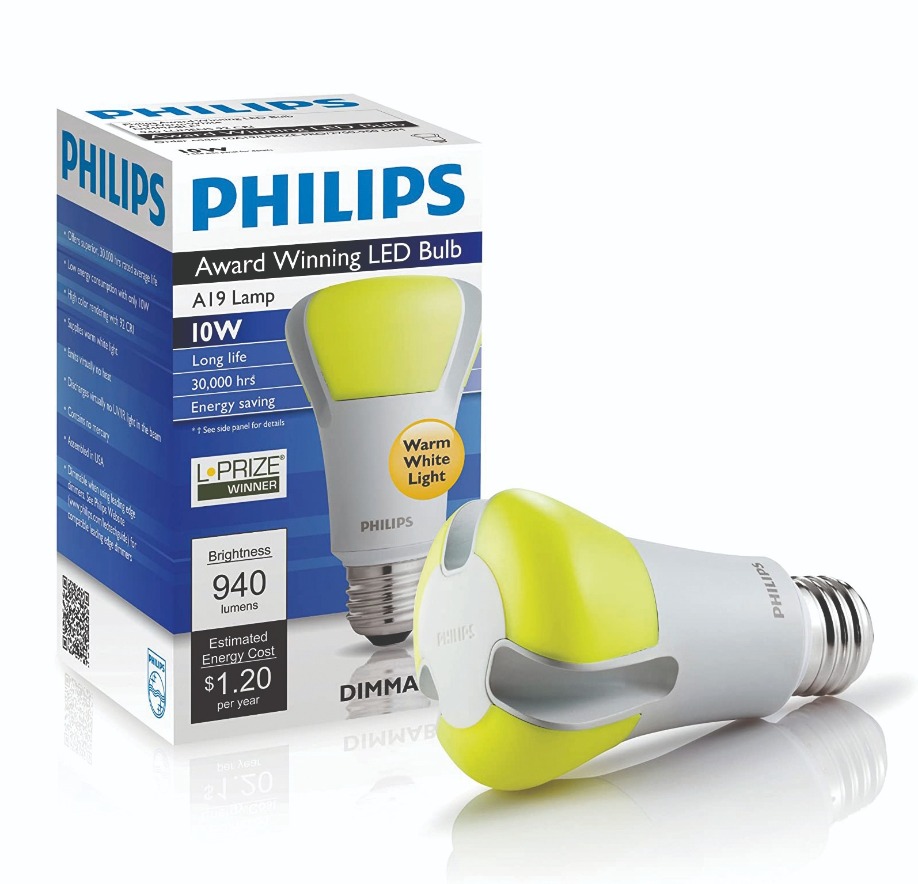
The 60 W incandescent bulb has many great attributes: instant on, a nice warm hue, and the opportunity to dim output. The $10 million L-Prize challenged makers of LED bulbs to replicate all these merits, while drawing less than 10 W. Philips Lumileds got their first, before launching their award-winning bulb. One striking feature of this award-winning source is the yellow colour of its emitting surface, easily visible when the bulb is not on. The yellow is associated with the remote phosphor, which when pumped with a battalion of 18 LEDs, casts a room in uniform, warm shade of white light.
Hero results pique interest but don’t guarantee sales. That’s because designers want products that combine a great performance with longevity.
Developers at Transphorm understood this completely. They knew their GaN FETs were attracting much attention because they were a promising product, exceeding the efficiency of silicon and coping far better at elevated temperatures. However, to win sales, Transphorm had to assure potential customers that they should not have any concerns over reliability, so they put this 600 V FET in for independent device testing. This device passed to give Transphorm, in 2012, the industry’s first GaN FET qualified to the JEDEC standard.
Initial products by this West-coast firm were produced on SiC substrates. But production soon switched to silicon. Merits of this move were not limited to a cheaper, larger foundation, but included the opportunity to process devices on mature 200 mm lines, potentially in under-utilised fabs.
Efforts at proving device reliability continue. Transphorm’s GaN-on-silicon FETs are now qualified at standard temperatures and 175 °C, helping to drive sales, which surpassed 500,000 last November. Fourth-generation products launched this April have taken performance of GaN-on-silicon FETs to a new high and helped increase penetration into markets that include power supplies for computers and passenger planes, servo motors, and electric-vehicle on-board chargers.
Would it ever be possible to draw the debate on droop to a close? Given the competing, vigorously defended theories, it would require irrefutable proof. Obtaining this would not be easy, but in Spring 2013 claims of a smoking gun surfaced from a partnership between researchers at the University of California, Santa Barbara (UCSB), and the École Polytechnique in France.
This team’s evidence came from an extremely elegant experiment that drew parallels with that made by Robert Millikan at the start of the twentieth century. Millikan studied the photoelectric effect by measuring the kinetic energy of electrons exiting a metal bombarded with beams of photons.
On this more recent occasion researchers injected carriers into the quantum well and recorded two phenomena: the light emitted by the LED, and the energy of electrons exiting through the p-side of the device. To ensure all thermalised electrons left the LED, the p-side surface had been treated with caesium.
As the scientists from this collaboration cranked up the current through their device, they detected higher energy peaks, associated with the vacuum-emitted electrons. According to them, this observation provided unquestionable proof that Auger is the cause of droop. In their view, no other mechanism could be responsible for these ‘hot’ electron peaks. Strengthening this claim, they found that when droop kicked in, high energy peaks started to emerge.
So, did other researchers working in this field raise a glass, toast this team’s success and agree that this work had put the debate on droop to bed? Absolutely not. In general, those that are trying to fathom the cause of droop have entrenched positions and are convinced that after examining all the evidence the theory they postulated is still the most convincing.
Critics argued that the experimental results may have been interpreted incorrectly. Boston University’s Enrico Bellotti claimed that the experiment suggests that electron leakage is the cause of droop, with some help from the Auger effect.
Fred Schubert from Rensselaer Polytechnic Institute in Troy, NY, tended to agree, suggesting that some electrons detected in the experiment might not be associated with the Auger effect at all, having simply leaked out of the LED’s quantum well. Another reason why Schubert struggles to view Auger recombination as a major contributor to droop is that he considers droop to be stronger at low temperatures, while Auger is weaker.
The team from UCSB and the École Polytechnique addressed their critics in the November & December 2013 edition of Compound Semiconductor magazine. In their feature, they argued that in their LEDs, the electric field is not strong enough to cause electron leakage. They also countered claims that it would not be possible to observe Auger-generated electrons escaping into vacuum, and expressed concerns related to a claim that free-carrier absorption could be a cause of droop.
Discussing competing theories will have helped to progress efforts to come to a consensus on the cause of droop. But even now, the debate has not completely disappeared.
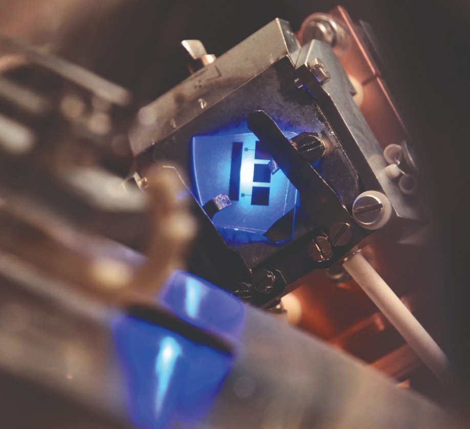
By tracking the energy of non-radiative electrons that pass through an LED while simultaneously recording the light output of this device, researchers from the University of California, Santa Barbara, and the École Polytechnique, France, claimed they had definitive proof that Auger is the cause of droop.
The prospects of emerging devices can be judged by the actions of the biggest players manufacturing products with the incumbent technology. If alternatives have an outside chance of success, a few leading firms might dabble in them; and if they are certain to play a major role, multi-nationals will invest, either through acquisitions or internal development.
Judged in this manner, wide bandgap technology is assured of an important role in the future. All the leading firms in the power electronics sector have branched out from considering only silicon devices, and made headway with either SiC or GaN.
In the case of Infineon, it’s not hedging its bets as to which of these two rivals is going to play a bigger role. Instead, it is pursuing both, viewing GaN as a strong candidate for below 600 V and SiC as the best option for higher voltages. Infineon did not embark on an internal development programme for GaN, instead deciding to acquire this technology. In 2014, it agreed to shell out $3 billion in cash for GaN-on-silicon pioneer International Rectifier (IR). Note, however, that as well as gaining IR’s GaN-based technology, it also picked up its low-voltage silicon MOSFET family, which accounted for the lion’s share of sales. When Infineon took IR into its fold, it viewed GaN-on-silicon as a long-term investment, generating sales at least five years down the line.
In March 2015, Infineon deepened its involvement in GaN, teaming up with Panasonic. This duo signed a deal committing them to jointly develop devices that combined Panasonic’s normally-off GaN-on-silicon transistors with Infineon’s surface-mounted packages that would house these chips.
More recently, Infineon has broadened its portfolio of CoolGaN products, made using its own devices. So GaN is underway and SiC and silicon are well established, giving this German powerhouse an incredibly broad portfolio.
In 2014, Infineon agreed to purchase International Rectifier for $3 billion. Orchestrators of the deal were Reinhard Ploss (left), CEO of Infineon Technologies, and Oleg Khaykin (right), President and CEO of International Rectifier.
During the last 25 years, the two biggest sectors within our industry have headed in very different directions. In the late 1990s five LED chipmakers rose to the fore – Nichia, Cree, Lumileds, Toyoda Gosei and Osram – and all have held on to one of these top spots for many years. Today they are still active, shipping high volumes, but their collective share is in decline, now accounting for less than half of the $20 billion LED chip market.
In stark contrast, the GaAs microelectronics industry, second in revenue to only the LED sector, has seen a dramatic contraction in the number of competitors, despite a growth in revenue over the last 25 years from below $0.5 billion to around $8 billion.
Big players that have left this industry include Anadigics, snapped up in 2016 by II-VI after spending its last few years converting its RF line to the production of VCSELs. Other leading names have merged.
In 2002, Skyworks formed through the marriage of Alpha Industries and Conexant, and more recently Qorvo emerged from the union of two heavyweights, RFMD and TriQuint. This new entity started trading on 1 January, 2015.
That merger had much going for it. Many viewed the two companies as complementary, with RFMD having greater strength in RF technologies for handsets and TriQuint offering a better portfolio of defence products.
Investors clearly approved of the union, with the share prices of both firms enjoying double-digit jumps on disclosure of the plans.
The new entity had the potential to net an annual revenue of just over $2 billion; and thanks to synergies providing yearly savings of $150 million, gross and operating margins were tipped to be 45 percent and 25 percent, respectively.
Five years on, has the merger delivered on all those promises? Well, sales for fiscal 2020, finishing on 28 March of this year, amassed $3.24 billion, with gross and operating margins of 41 percent and 13 percent, respectively.
So sales are well above those expected in 2015, while margins are healthy, but not as high as hoped. Investors seem content with these figures – Qorvo’s share price is now just north of $110, up from $70, the value of this stock on its first day of trading.
If you are a regular reader of this magazine, then by the middle of the last decade you would have been aware of the tremendous promise of gallium oxide. With a whopping bandgap of around 5 eV – the precise value depends on the particular polytype – it has the potential to deliver a knockout blow to those two blossoming middleweights, SiC and GaN.
Thanks to gallium oxide’s far wider bandgap it should be able to reign supreme in that most valued of characteristics, the on-resistance as a function of breakdown voltage. But that’s not its only alluring attribute: it offers versatility, because a thin film of gallium oxide can be deposited by a variety of techniques, including MBE and MOCVD; and there are several options for the substrate. Devices can be grown on sapphire or on gallium oxide, which could tumble in price, because boules of this material can be produced by melt-based techniques.
Gallium oxide’s great promise has had no trouble in attracting interest and initial investment. However, like any material, its first steps towards commercialisation hinged on demonstrations of device capability. They came thick and fast in 2016.
During that year two key breakthroughs emerged from a team at the Air Force Research Labs (ARFL). Using structures made from the β-polytype and grown on a native substrate, engineers working there grabbed
the limelight by producing a MOSFET with a record-breaking critical field strength of 3.8 MV/cm – that’s about four times the critical field strength of GaN. And later that year they realised another breakthrough, reporting the first ever enhancement-mode FET with a high-breakdown voltage in the off-state. This second success demonstrated that a lack of p-type carriers in gallium oxide is not a show-stopper to making a normally-off FET.
The gallium oxide research programme at ARFL had been inspired by the work at Japan’s National Institute of Information and Communications (NICT). Researchers at NICT, working with domestic partners, had driven much early progress in both materials and devices, and gone on to produce the world’s first MESFETs and MOSFETs in 2012.
Four years down the line refinements to NICT’s MOSFET, which included the addition of a field plate, had bolstered the breakdown voltage to just over 750 V, a result that is still impressive today.
Japan also provided another milestone in gallium oxide. In 2016, using a novel growth technique known as mist epitaxy, researchers at Flosfia reported a-Ga2O3-on-sapphire Schottky barrier diodes sporting an on-resistance that trumps state-of-the-art variants made from SiC. This spin-off of the University of Kyoto is commercialising these ultra-wide bandgap diodes, along with accompanying MOSFETs. Production ramps are slated for this year.
What is the most famous valley in the world? OK, it might not be the first answer to trip off your tongue, but a great case can be made for Silicon Valley.
While this region may not have that many fabs today, the engineers that worked here – many of them graduates of Stanford University – are to be thanked not only for their advances in technology, but for giving all of us that work in the semiconductor industry a higher status in society. Today technology is admired, benefitting many, even if the average man in the street has never heard of holes, bandgaps or lithography.
California is not the only part of the world with a cluster of semiconductor companies. They are also found in Leuven, Belgium; in Dresden, Germany; in Eindhoven, The Netherlands; and in Grenoble, France. Together, clusters comprise 800 companies and account for 150,000 jobs. By having many firms nearby, often operating at different positions within the supply chain, they support one another while attracting more engineering talent to the region. This helps to increase the kudos of the clusters, bringing in yet more business and innovation, while fostering an entrepreneurial outlook that gives local start-ups the best chance of thriving.
Efforts to create the world’s first compound semiconductor cluster can be traced back to 2011, when IQE’s charismatic leader, Drew Nelson, met the economic minister for Wales at that time. Nelson put the case for a far stronger infrastructure within the UK to support the compound semiconductor industry. Back then, IQE had virtually no domestic customers. That’s not to say, however, that IQE was the only company in South Wales working in our industry: this part of the UK was and continues to be home to etching and deposition tool maker SPTS, and a Microsemi facility with packaging expertise.
Nelson’s next steps included working within a group set up by the European Commissioner for Technology for the Digital Economy. Involved in a team considering key enabling technologies, Nelson championed the construction of a sovereign capability for compound semiconductors in South Wales to rebuild the continent’s manufacturing capability for this technology.
Building on these efforts, Nelson lobbied the Welsh Government and Cardiff University to set up an Institute for Compound Semiconductors. He had a vision for a local facility, delivering cutting-edge technology, developed using tools and processes compatible with high-volume manufacturing. In March 2015 the UK Government funded this initiative, and a year on planners gave the go-ahead for the construction of a new building for the Institute for the Compound Semiconductors. Forming part of the new Innovation Campus, the Institute is slated to open late next year.
To help commercialise the technology developed at the Institute for Compound Semiconductors, in 2015 IQE and Cardiff University founded a joint venture: the Compound Semiconductor Centre. Using funding from Cardiff University and some equipment from IQE, it runs collaborative research projects.
In 2016 that year, more links were added to the supply chain. In January, the UK government stumped up £50 million, funding the creation of a Compound Semiconductor Catapult, an open access R&D facility focused on helping UK businesses exploit advances in compound semiconductor technologies. And later that year the UK’s Engineering and Physical Sciences Research Council poured £10 million into a Manufacturing Hub for Compound Semiconductors, targeting the translation of research into high-volume chip manufacturing.
With many pieces of the jigsaw now in place, in summer 2017 the cluster officially opened for business, taking the name CSconnected and holding events with speakers from all key stakeholders. The cluster also took a huge leap forward, grabbing an opportunity to get its hand on a production line. The 200 mm silicon fab in Newport, South Wales, had come into the hands of Infineon through its acquisition of International Rectifier. After the German powerhouse evaluated its global chip manufacturing capabilities, it viewed the Newport Fab as surplus to requirements. This facility was put up for sale, with Nelson leading a private equity buyout. Emerging from this deal, Newport Wafer Fab had guaranteed orders from Infineon for two years.
Further ahead, those in the cluster hoped that the lines would also be used to produce compound-semiconductor-on-silicon chips. This fab has a track record in processing GaN-on-silicon devices, produced during International Rectifier’s tenure, but other material systems are possible. Such efforts will be aided by IQE’s acquisition of Translucent, a developer of rare-earth oxides, which can provide a bridge between a silicon wafer and compound semiconductor epilayers.
Those within CSconnected are continuing to advance. The CS Catapult has moved into part of a very large building constructed for LG Semicon, with IQE taking the remainder, using it to create an epifoundry that could house up to 100 MOCVD tools. The cluster has also expanded to include Swansea University, which is constructing a Centre for Integrative Semiconductor Materials. Such activities will continue to create job opportunities and swell revenues. According to a report published last August by Cardiff University, the cluster now accounts for more than £460 million in sales and nearly 1500 jobs. That’s a good start towards a very long-term goal of eventually creating 5,000 positions in the compound semiconductor industry.

Construction of the Institute for Compound Semiconductors is well under way, and should be completed next year.
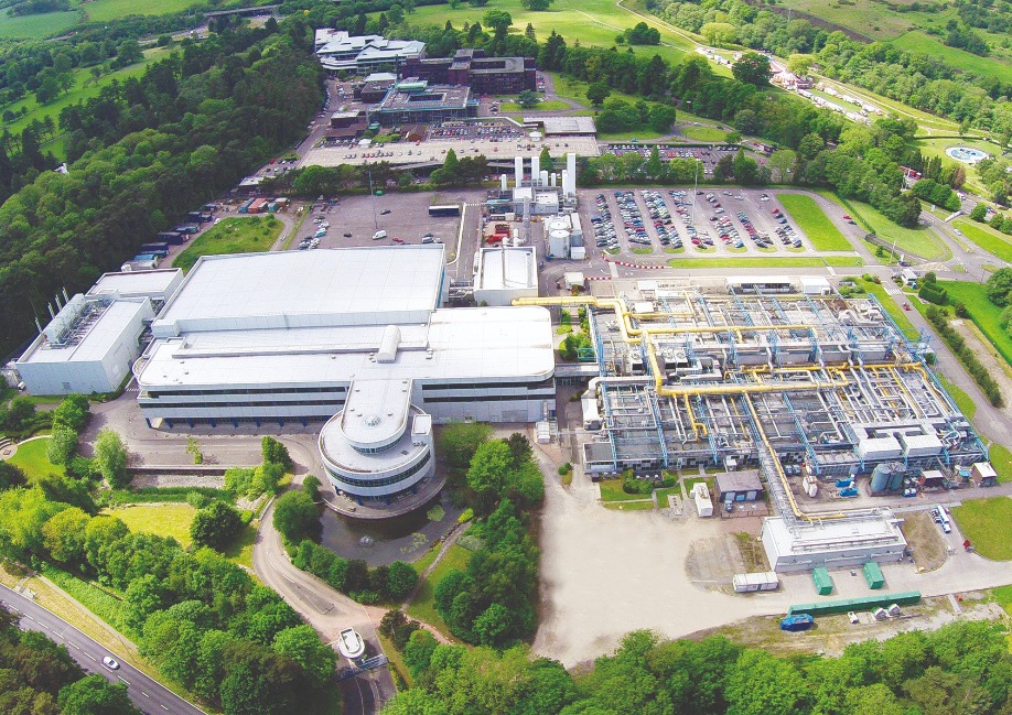
CSconnected, the world’s first compound semiconductor cluster, opened for business in 2017. By the end of the year this cluster, based in South Wales, had strengthened its capabilities, thanks to the launch of Newport Wafer fab, a facility Infineon deemed surplus to its requirements.
The VCSEL has some wonderful strengths. It is efficient, allowing it to run off a battery; it can be turned on and off at very high speeds, making it a great source for transmitting vast amounts of data; by adjusting the size of the aperture, it allows single-mode emission with a circular profile, simplifying optics; and it is well-suited to high-volume manufacturing, partly because its design allows on-wafer testing.
However, there is room for improvement. Despite decades of development, the VCSEL spans a far narrower range of wavelengths than edge-emitting lasers and LEDs. Expansion of the spectral domain has been very slow, given the long history of this device. Its roots go back as far as 1965, when Ivars Melngailis, working in the MIT Lincoln Lab, announced a ‘longitudinal injection laser’ emitting at 5.2 μm. This device, formed from an InSb diode and featuring polished top and bottom surfaces to ensure optical feedback, was incredibly impressive feat for its time, but is far from practical. Lasing required a hefty 20 A drive current and cooling to 10K.
The first real VCSELs came from the labs of Kenicha Iga from Tokyo Institute of Technology. In 1977, Iga proposed a design that shares many of the features of today’s VCSEL. For the next 11 years he almost singlehandedly pioneered this class of device, before other groups noted his breakthrough and redirected their efforts towards this technology. Success followed, with research in the latter part of the twentieth century initially focusing on the near infrared, before attempts were made to widen the spectral range of the VCSEL in both directions.
Initially, breakthroughs with the GaAs-based material system enabled 850 nm and 980 nm VCSELs, before further progress stretched emission to around 650 nm. Wafer-fusion brought yet more success, allowing GaAs-based mirrors to be united with InP-based active regions to realise emission at 1.5 μm.
By the turn of the millennium, researchers started to consider the next goal: expanding emission to the blue and green. Success would open up new markets, allowing devices to be deployed for high-resolution printing, high-density optical data storage, chemical and biological sensing, full-colour displays and lighting.
Producing VCSELs operating in this spectral domain is far from easy. To reach these shorter wavelengths, the GaAs-based material system has to be replaced with one based on GaN and its related alloys. The switch may sound a simple, but it’s anything but.
The biggest issue is producing the mirrors that sit either side of the active region. This is relatively easy in a GaAs-based VCSEL, because this material system is blessed with the pairing of GaAs and AlGaAs. These III-Vs have very similar lattice constants, so strain is not an issue, and there is a significant difference in their refractive index, aiding reflection. When 20 pairs of alternating layers of GaAs and AlGaAs make a mirror, it has a reflectivity of 99 percent, sufficient to make a high-performance VCSEL.
For blue and green VCSELs, to prevent strain from degrading the mirrors, GaN has to be paired with Al0.83In0.17N, a trickier alloy to grow that has a relatively low refractive index contrast. Growing two sets of GaN-based mirrors takes too long, so it is better to combine a nitride-based bottom mirror with a top one based on dielectrics, an approach pioneered by Nicholas Grandjean’s team at EPFL. Their high-point came in 2007 when they reported the first optically pumped GaN VCSEL. Frustratingly, funding dried up for Grandjean, with those holding the purse strings arguing that the first electrical GaN VCSEL would come from Japan. They were more or less right, and now we will never know if Europe could have beaten them to it.
The first GaN VCSEL actually came from National Chiao Tung University, Taiwan, announced in April 2008. This device required cryogenic cooling, a restraint overcome later that year by Nichia, using a pair of dielectric mirrors. Nichia persisted with this design, increasing the output power to 0.62 mW in 2009, before making further minor but additional gains. But the lack of substantial progress appears to have curtailed further GaN VCSEL development by the Japanese chipmaker. Nichia never came close to 10 mW, the ballpark figure for augmented-reality devices, projection systems and displays. That milestone came in 2018, achieved by two Japanese companies working independently. Stanley Electric, partnering with Tetsuya Takeuchi and his team from Meijo University, built on the work at EPFL, improving the growth conditions. In the autumn of that year they reported a blue VCSEL with an output in excess of 15 mW. And in November 2018, Sony unveiled a 12 mW VCSEL with a novel design, featuring a far larger cavity that incorporated a thinned GaN substrate, and a curved mirror grown on the backside of the wafer.
Alongside these breakthroughs in blue VCSEL performance, 2018 will be remembered for the market success of the infrared cousins. Up until then, datacoms provided by the primary revenue stream for this device, but in 2018 the market for handsets caught up, according to Pierrick Boulay, Technology and Market Analyst at Yole Développement.
A year before, Apple had launched iPhones incorporating VCSEL-based sensing, and in 2018 it became the main consumer of these lasers in smartphones. Although VCSELs were also featuring in 2018 models made by Xiaomi, Vivo, Huawei and Oppo, they were far less popular with consumers. Initially, Apple bought its VCSELs from Lumentum. But in late 2017 the technology giant decided that it needed to secure a second source, so dangled a carrot at Finisar, promising orders for $390 million of VCSEL products. Qualifying this device took time and did not dent Lumentum’s orderbook in 2018.
Boulay predicts strong growth for VCSELs, as they will see increasing use in smartphones, continued deployment in datacom networks, and start to feature in sensing applications covering greater distances, such as automotive LiDAR. The market for these surface-emitting lasers is expected to mushroom from $738 million in 2018 to $3.7 billion in 2024.

Facial recognition offers a lucrative market for the infrared VCSEL.
To secure a second source for VCSELs, Apple agreed to purchase $390 million of these devices from Finisar.
In spring 2019, Cree, the developer of SiC substrates and various optoelectronic, RF and power devices, re-aligned its business in emphatic fashion. It’s relatively new CEO Greg Lowe had no qualms in carving off the company’s Lighting Products division to Ideal Industries; giving the LED business that brought so many years of success a back seat; and focusing on wide bandgap materials and RF and power devices.
Helping to have made this monumental decision would have been a number of lucrative SiC wafer supply deals: contracts with Infineon, ST Microlectronics and other companies totalled $500 million.
By summer 2019 Cree’s LED business had softened and it had netted the lion’s share of its $310 million sale to Ideal. These circumstances would have helped Lowe to move forward with his vision, investing $1 billion in massive expansion of SiC capacity. A state-of-the-art, 200 mm facility would be built by 2024, delivering a 30-fold expansion in capacity compared with the first fiscal quarter 2017.
Later that year Cree had an offer it could not turn down – a $500 million grant from the state of New York. Instead of having to spend $450 million retrofitting an existing structure at its headquarters in Durham, NC, it could now invest $170 million in building a new, automotive-qualified 200 mm power and RF wafer fabrication plant in Marcy, New York.
The new building should be up and running in 2022, initially using 150 mm wafers before transitioning to 200 mm wafers two years’ later. Until that comes on line, capacity is being increased at the headquarters.
Since these announcements, the proportion of revenue coming from the less profitable LED products line has continued to decline, while that from the Wolfspeed division – it encompasses SiC wafers, power electronics and RF devices – has seen revenue grow. Sales are currently taking a knock from the Covid-19 epidemic and trading restrictions with China, but the long-term prospects for Cree are very, very good.

Supported by a $500 million grant from the state of New York, Cree/Wolfspeed, is building a new automotive-qualified 200 mm power and RF wafer fabrication plant in Marcy, New York, that should be up and running in 2022.
What will this year be remembered for? With several months still to go it’s not yet clear, but within our industry let’s certainly hope it’s not for Covid-19. Fabs are running, and while business is impacted, compared to many sectors of the economy we are relatively unscathed.
It’s quite possible that 2020 will go down in history as the year when microLED displays started to gain traction. Making them is not easy, as it tends to involve moving millions of micron-sized LED chips from their wafers to a display backplane, while ensuring zero duds. But these efforts are rewarded, with the resulting displays delivering ground-breaking brightness, incredible efficiencies, exceptional levels of contrast and freedom from burn-in.
A tremendous amount of money has already been pumped into microLED technology. According to
Yole Développement, funding to date totals $4.8 billion. Of that, Apple accounts for $1.8 billion, a figure that includes the Luxvue acquisition and internal development.
Facebook is another tech titan with ambitions of using microLEDs in its future products. It is partnering with Plessey, a UK company that has overcome issues of mass transfer by producing its LEDs on GaN-on-silicon wafers subsequently bonded to a silicon backplane. Making blue and green LEDs with GaN is well-known, while red is far more challenging. However, last December Plessey announced that through strain engineering it had realised red emission from this class of device, opening the door to a new way to make full-colour displays.
MicroLEDs also have opportunities outside of displays. This summer engineers at CEA-Leti have broken the record for data transmission for LiFI, using a 10 μm microLED to transmit at 7.7 Gbit/s. This method of transmission can guarantee secure communication within a room, a feature not offered by WiFi or 5G.
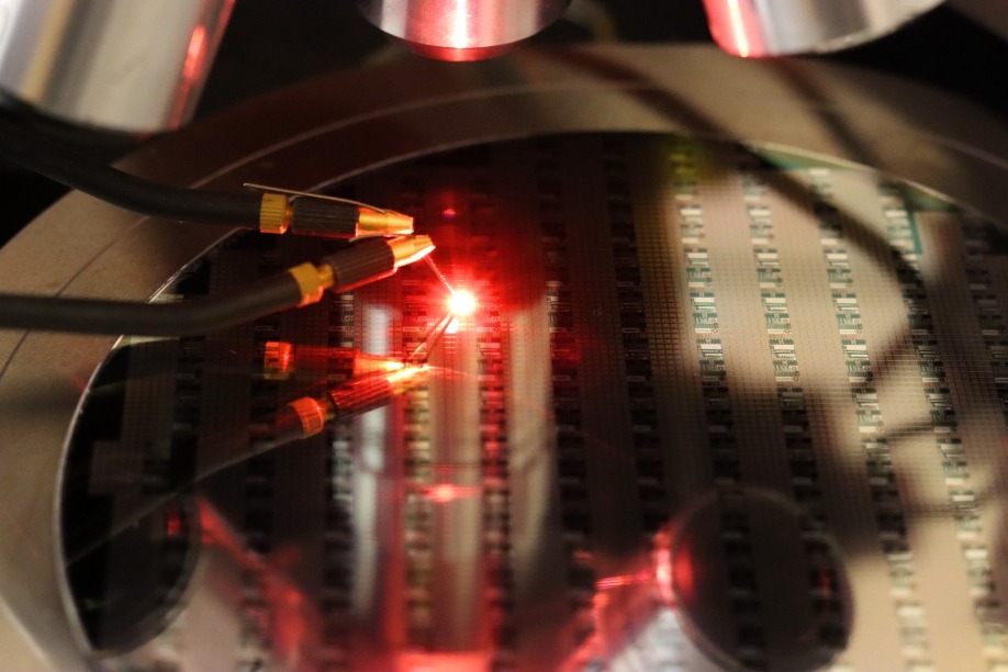
By straining its GaN-on-silicon LEDs, Plessey can produce red, green and blue emitters on the same wafer. This aids the creation of a full-colour microLED display, a technology that has enabled Plessey to team up with Facebook.
Our industry will have expanded its reach by the time Compound Semiconductor celebrates its fiftieth anniversary. Come that milestone, chips made by our industry will be behind: widespread air, water and surface disinfection; superior displays; incredibly efficient power supplies; and breath-taking data rates
BY RICHARD STEVENSON
I EXPECT THAT YOU, like me, are annoyed by the oft-repeated quip ‘gallium arsenide is the material of the future and always will be’. That view surely smacks of ignorance. Those that say such things are clearly unaware of the GaAs-based laser diodes in their CD and DVD players, the high-power variants used to cut and weld metals that form the skeleton of their cars, and the GaAs HBTs that amplify the RF signal within their smartphones.
However, while some of those working within the silicon industry may irk us all – whether we are part of the GaAs industry, or a sector involved in the manufacture of InP, GaN or SiC chips – we have to admit that we can learn a lot from them. The reality is that those of us that work in compound semiconductor fabs dream of replicating the maturity of their technology, their understanding of reliability, and their low levels of defects.
Another lesson we can learn from the silicon industry is that if we plot the rate of success to date and extrapolate this, we see what the future holds. It’s a point well-illustrated by Moore’s Law, a rate of progress that has been maintained for decades. Even when continual success seems unlikely, with further miniaturisation throwing up issues with no obvious solutions, progress has continued at historical rates.
We can also plot progress in our industry. This gives us the opportunity to not only look back at how far we have come, but see where we might be in the future. Using this approach we can take an educated guess at not only where the performance of compound semiconductor chips could be in the future, but also the advances in the technology they support.
In the LED industry, progress follows Haitz’s Law, which states that with the passing of every decade, the cost-per-lumen plummets by 90 percent and the output of a packaged LED climbs by a factor of 20. It is this rapid rate of progress in the bang-per-buck that has enabled white LEDs to move on from their first killer application of providing illumination in the handsets to backlighting screens and eventually providing general lighting. Over the next few years, further falls in the price-per-lumen will help LED lighting become the incumbent technology everywhere. Revenue for this sector is tipped to climb, but the LED light bulb is arguably now a commodity, offering razor-thin margins to chipmakers.
An emerging opportunity for visible LEDs is in displays made from microLEDs. This application, which could net billions and billions of dollars, will be helped by a fall in the cost-per-lumen. However, if this type of display is to become commonplace, a breakthrough is needed in the efficient mass transfer of the tiny chips that create the pixels. It’s a problem that has been grappled with for several years, and there are some promising solutions, such as eLux’s microfluidic technology – but more progress must follow if this is to become the next killer application.
LED on Mars
For deep-UV LEDs, if progress continues to follow Haitz’s Law, these devices will be everywhere by the time Compound Semiconductor celebrates its 50th anniversary. By 2045, packaged deep-UV LEDs could deliver several hundred watts of power, at a cost of just a dollar-per-Watt, thanks to improvements in the chip’s design, its package and the way it is driven.
If that happens, today’s incumbent source of deep-UV emission, the mercury lamp, will be relegated to museums. By then, the UV LED will be the dominant technology for purifying water and disinfecting surfaces and air, and it will also be deployed in numerous processes involving the curing of adhesives. Some devices may even be on Mars – NASA has manned missions slated for the 2030s, and even if there are delays, there is a good chance that within the next 25 years deep-UV LEDs will be purifying an astronaut’s drinking water on the red planet.
The coming decades should also witness a steady increase in the efficiency of blue lasers. While blue LEDs can operate with wall-plug efficiencies exceeding 70 percent, today’s best single-mode blue lasers are only operating in the high thirties, and their multi-mode variants in the mid-forties. Both figures are on the rise, and even if the rate of improvement is not maintained in the coming decades, efficiencies could still exceed 70 percent by 2045.
What would be the implications of such efficient emitters, which have the added benefit of easing thermal management? There is sure to be a rise in the use of these sources for processing copper and other yellow metals, because these materials have an absorption sweet-spot in the blue. In comparison, when today’s more common infrared lasers are used to process yellow metals, this leads to sputtering and ultimately inferior welds.
In addition to a hike in sales for material processing, driven by the growth in electric-vehicle production, blue lasers are tipped to see increasing use in colour projectors. Insufficient brightness has held back sales, but the opportunity to dispense with a backlit screen is a major asset in both the home and the office. Efficient green lasers are also needed. While they lag those in the blue, they are also improving, and they don’t need to be quite as efficient, because they operate at around the eye’s most sensitive wavelengths.
Given the merits of on-wafer testing, a circular emission profile and a very high modulation rate, the next 25 years should witness growth in shipments and spectral coverage of the VCSEL. Over the next few years, infrared variants will gain greater deployment in smartphones, where they support facial recognition, and further ahead in vehicles, providing a light source for LiDAR. GaN-based blue and green VCSELs are still in development, but there is no doubt that they will move into production, probably initially as sources for car headlights. By 2045, they should have entered other markets, possibly including displays.
Multi-junction missions
In the next few years many satellites are going to be launched. Contributing to this hike is the SpaceX Starlink programme, aiming to create a network of 12,000 small satellites by 2027. The satellites will form the backbone of global broadband internet.
Such efforts will provide much business for makers of multi-junction solar cells. Although these devices are pricey, the higher efficiency and great robustness to radiation allow them to monopolise this market. The efficiency of these cells is increasing, but gains are not easy to come by. One option currently being explored is to concentrate sunlight, an approach that can deliver a substantial gain.
Efforts at concentrating sunlight previously offered much promise for the creation of a terrestrial industry, before hopes were dashed by a dummy whammy: plummeting silicon prices; and a financial crisis, which starved fledgling firms of much needed investment. Far fewer teams are now battling for the bragging rights that come from having the most efficient cell – a potential solution to cutting costs – but records continue to rise. Leading the way is a team from NREL, pursuing a six-junction design. This device has an efficiency of just over 47 percent, and if its resistance can be reduced to that found in four-junction variants, this architecture could break the 50 percent barrier.
Further gains are possible, with values of just over 60 percent a realistic upper limit. Given the slow progress with silicon cells, that would be more than double the record value for the incumbent technology. But even an advantage that significant is not necessarily going to lead to a re-birth of the terrestrial CPV industry, which is in a catch-22 situation. For costs to come down there needs to be economies-of-scale, alongside refinements coming from insights associated with significant production volumes. Could that come from CPV in space? If it does, and the power generated per unit area comes to the fore as a key metric in sunny climes, CPV stands a chance of being a big industry by 2045.
SiC, GaN and gallium oxide
In the wide bandgap industry, progress is fast, spurred on by Cree’s $1 billion investment in SiC that will increase its capacity by a factor of 30 between 2017 and 2024. Many of its SiC devices will be deployed in electric vehicles, which will become more common as governments all around the world look to trim their carbon footprints. Shipments of GaN-on-silicon power devices are also tipped to take off. Operating at lower voltages – initially 600 V and below – they will enable an increase in the efficiency of numerous forms of power supply. Further ahead, GaN CMOS should start to appear, leading to further gains in circuit efficiency, realised with smaller, lighter-weight units.
However, by 2045, these middleweights – and that is how we should look at GaN and SiC – could well be in decline. By then, they could be overtaken by gallium oxide, a heavyweight with many attractive attributes. Gallium oxide’s potential performance, judged in terms of Baliga’s figure-of-merit, is better by an order of magnitude, and the cost of manufacture will be competitive. Unlike SiC and GaN, native substrates can be grown by melt-based techniques, allowing production of competitively-priced devices with great crystal quality. Like GaN, transistor performance is impeded by difficulties in realising p-type doping, but engineers can turn to a similar trick to ensure success: use the work function of the gate to pinch off an array of fin channels. Another issue with gallium oxide is its low thermal conductivity, but again, the solutions adopted with other compounded semiconductor devices offer routes to success. By following in the footsteps of other parts of the wide bandgap industry, it is possible that gallium oxide devices will take less time to get to market, and undergo a faster ramp to production volumes.
The shape of 7G
Based on historical rates of progress, which indicate that it takes about a decade to migrate from one generation of mobile technology to another, we should have 7G well established by 2045. If this happens, one can envisage incredibly fast data rates, possibly at hundreds of gigabits per second, using transmission in the terahertz domain.
But is it inevitable that we shall have this technology? Some well-informed sceptics suggest not, offering a range of compelling arguments based on market economics. Many of us are upgrading our smartphones far less frequently than we used to, because the latest models offer only incremental benefits – maybe a better camera, or water-resistance. Often we are reluctant to pay high fees for call plans, and so it’s hard for carriers to grow their revenues. The problem is essentially that as time goes on, we expect more while paying less. With that mindset at play, carriers should be reluctant to invest in any new generation of technology. And this concern should be magnified, because the roll-out of successive generations of technology is now getting more expensive. New generations of mobile technology operate at higher frequencies, where attenuation is higher. As increasing the transmission power is not a viable option – regulators are unlikely to approve, and a hike in power would be detrimental to battery life – the solution is to go to smaller cells, and this increases roll-out costs.
One may also wonder why anyone would need these breath-taking transmission speeds. It makes no sense to watch a broadcast in ultra-high-definition on a portable device with a small screen. Maybe ultra-fast data rates would be used for remote robotic surgery, but that is hardly a mainstream application. So, if most of us can’t see the need for super-high speeds, why would we ever be willing to pay extra for them? The threat is that carriers will never recoup their investment.
But maybe we are not looking at this in the right way. Back in the 1990s, when the much-lamented Word 5 provided the jewel in the Microsoft suite, there didn’t seem any need for more computational power, either in speed or memory. But if we were to try and use those machines today, they would feel very clunky and fail to cope with our high-res photos, digital downloads and so on. The extra levels of computational performance have been used in ways that we value today, but had not been envisaged.
Right now, the Covid-19 pandemic has shifted the world of work. While we might now get into the office, if we attend a conference, it’s probably involving logging on and listening to presentations. It’s a poor second to being there, as we can’t interact with the same level of intimacy as before. For example, we can’t pick up on body language. However, suppose we had ultra-fast communication, offering a more immersive experience involving some form of virtual reality. This could be so beneficial that companies would be willing to pick up the tab for the connection, reasoning that it offered a good return for an outlay far less than plane tickets and hotel bills. It would also help to trim carbon footprints, an issue that may be taken more seriously in the 2040s.
If 7G does roll out before this magazine celebrates its fiftieth anniversary, it will surely be good news for our industry. Whether communication occurs high in the gigahertz realm, where there is plenty of space, or in the terahertz domain, compound semiconductor devices are sure to features in handsets and infrastructure. GaAs may still dominate, but it could lose out to InP, the king of speed within the III-Vs.
Successes in this sector, plus those in power electronics, satellites, displays and disinfection, suggests that even those in the silicon industry currently failing to appreciate the benefits of compound semiconductors today should have started to change their mind well before 2045. Compound semiconductor devices are already pervading society, and in 25 years’ time the role they play will be even more significant.
From flat panel displays to semiconductor wafers, the use of indium in electronics continues to grow.
By Robert Ploessl, Indium Corporation
The element with atomic number 49 – indium – is central to modern life. Just consider a typical day: often we will spend hours staring at a flat panel display containing hundreds of thousands of pixels, each turned on and off by thin-film transistors and illuminated by some form of LED. While these transistors and LEDs might contain indium, there is no doubt that this element is encountered by the light traversing the display stack, as it will pass through indium-tin oxide (ITO) electrodes. This oxide combines transparency with conductivity, making it a great material for the display industry. In some of the latest high-colour-gamut TVs, indium crops up again, appearing in the display’s InP quantum dot layer of the colour filter that yields brilliant reds and greens. This makes five potential encounters between photons and indium-based materials before the light hits our retina. And there may be even more. If we watch content stored remotely, such as streaming video, it will reach us through a network of optical fibres, transmitting infrared light generated by an InP-based laser.
For those of us that are reading this on an electronic screen, the chances are that most of the above applies – there is no doubt that indium seems to be everywhere. Yet, despite its ubiquity, the economics of indium are poorly understood. That’s because most of the building blocks of modern technology emerge from supply chains that are rarely discussed, even in the technical press. To put it frankly, most of us don’t have much of a clue where indium comes from.
Let’s go back to the beginning. Like all heavy elements, indium was created during supernovas as planets condensed and formed. Due to its geo-chemical properties, indium appears in sphalerite, the most common ore of zinc, where its concentration can be as high as 100 parts per million. Another common carrier element for indium is lead. Deposits containing relatively high concentrations of indium are found all over the world. According to an exhaustive survey detailed by Ulrich Schwarz-Schampera and Peter Hertzig in Indium: Geology, Mineralogy, and Economics, a large number of indium-bearing deposits have been found around the Pacific Rim and in many other sites in Europe, Africa, and central Asia.
It comes as a shock to many, including quite a few working within the semiconductor industry that there are no indium mines anywhere. Element 49 is almost always co-mined with zinc. That’s not actually too surprising, as there are only a few carrier elements that have their own corresponding production infrastructure, such as copper, iron, and aluminium. When demand swings for most co-mined elements, such as indium, supply at the carrier infrastructure is often relatively inelastic. The real supply for indium is actually set downstream from the mines at the refiners where material is processed to produce an indium content up to 4N (99.99 percent). Indium ore is found all over the globe but refiners are heavily concentrated in China.
The overall global abundance of indium is in the range of 5-7 parts per million. That may not seem like a lot, but it is almost exactly the same value as that for silver. However, unlike that precious metal, which has been in use since ancient times, indium only started its commercial life in the twentieth century and was initially explored for its mechanical properties. One of the first successful applications of indium began in the 1940s when engineers diffused this metal into the surface layer of the bearings in aircraft engine pistons. Indium provided lubrication on the atomic scale, reducing wear and tear on the engine and increasing fuel efficiency – a prime example of our strongly held belief at Indium Corporation that materials science changes the world.
Fast forward to the age of electronics and high-speed communication when InP semiconductor crystals came to the fore, thanks to a bandgap that matches the transmission window of optical fibre. With a light source and a lossless technology for transmitting information, the groundwork was laid for the Internet and the connection of computers. It is a success story that we all know.
The InP-based lasers in optical networks are built on wafers sliced from monocrystalline boules, which are grown using techniques such as vertical freeze gradient and the Czochralski method – both requiring high-purity indium ingots as the starting ingredient. It is not sufficient to use standard commercial indium metal, which has a purity that starts at a 4N. That purity is suitable for making inorganic compounds and ITO sputter targets, but is not nearly enough for the production of compound semiconductors, which require a purity at least 500 times higher, typically 6N5.
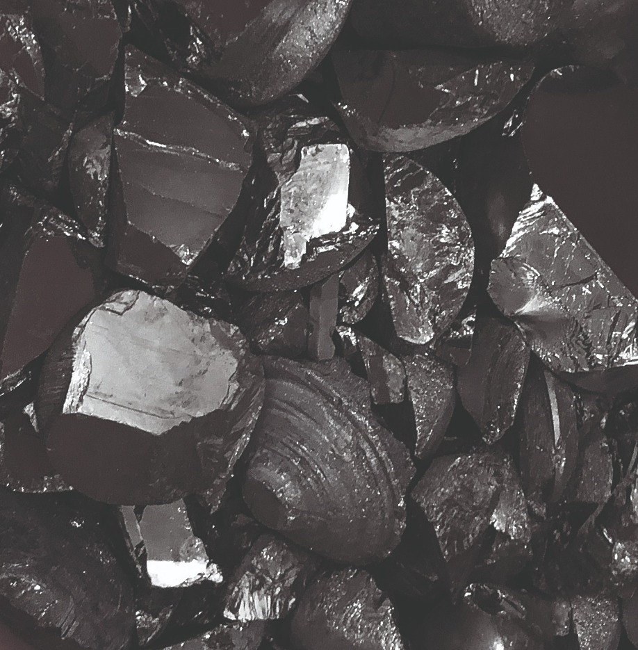
Indium phosphide crystal pieces from wafer boule manufacturing – the raw material for reclaiming indium from InP.
What happens to the InP crystals and wafers that are left over from their respective manufacturing process? What about the sustainability of the indium value chain?
From the start, the ITO and flat panel display industry have been reclaiming indium and the compound semiconductor industry is now following suit. This is to be expected, as every mature, high-value-added materials-using industry should have a recycling loop for its valuable input materials. At Indium Corporation we have added this reclaim capability, initially for InP crystals and wafers, and we plan to add capabilities for InSb in the near future.
There is no doubt that it makes sense to do this at the industrial level with end-of-life wafers and unused crystal material. It is harder to accomplish this with packaged electronic InP devices or end-of-life consumer products – this probably explains why we are not aware of any companies doing so. However, if our society is to be a responsible steward of our planet, this is an important objective.
As of today, we are concentrating on output from crystal growers, InP wafer makers, and output from fab and epi-wafer fabs. If you are using InP wafers in a fab and have any recycling needs, we certainly would like to hear from you.
So, what does the InP-consuming industry landscape currently look like and how has it evolved? 25 years ago, this magazine reported that global InP wafer consumption totalled 58,000 wafers, equating to a surface area of 183,000-square inches. Back then, Japan led the world and was responsible for 56 percent of wafer consumption. Today, according to a recent report from SEMI, 64 fabs are capable of processing InP wafers – 40 percent are found in North America, 31 percent in Europe, and the balance in Asia. This report claims that the capacity figure of all these InP fabs, based on 200 mm equivalent wafers, totals 667,000. That’s a figure that equates to just over 11 times that of global consumption in 1995. So, it is clear that there has been an astonishing growth of InP, even with the caveat that the SEMI figures are capacities, rather than actual output. They are total fab capacities; that is, the InP output is in the mix but not the total number.

Polycrystalline InP wafers form part of the input stream for indium reclaim.
Another use of indium is, of course, in indium-containing epilayers. They are grown epitaxially, often by MOCVD, using the metal-organic trimethyl-indium. This source is made from high-purity indium trichloride, available as an anhydrous salt. The density of this salt may be tailored to the process of our customers.
When engineers use trimethyl-indium to grow heterostructures by MOCVD, they control the flow of this source of indium. With this lever, they tune the band structure and shift the emission or absorption wavelength of a device. An exciting new development over the last few years is the development of hybrid integration, a technology that allows compound semiconductor layers to be constructed directly on a silicon substrate.
As this technology is still in its infancy, outside the display market the growth of indium consumption is largely driven by data centres. They are the workhorses for the cloud, which has become both the storage and the processor of internet core computing. The cloud holds messages, photos, videos; it hosts entire web sites; and it runs software algorithms like machine learning. And if you are reading this online, the article will be stored there and brought to you via InP lasers to a screen coated in ITO, probably backlit with InGaN-based LEDs.
U. Schwarz-Schampera, P. M. Herzig, Indium – Geology, Mineralogy, and Economics, Springer 2002
SEMI report: SEMI – Power & Compound Fab report 2013 to 2024Jan 2013 to Dec 2024, update April 24, 2020 Edition https://www.semi.org/en/news-resources/market-data

Double-layered NiO contact provides a great p-type layer
Engineers at Nanjing University, China, have poineered a new architecture for the Ga2O3 p-n diode. Their device features a double-layered NiO p-type layer.
Even without field plates and edge-termination structures, this new design is claimed to offer a higher breakdown voltage and a lower leakage current than comparable Ga2O3 devices based on either Schottky barriers or p-n junctions.
Spokesman for the researchers, Jiandong Ye, points out that the merits of their novel device are not limited to a high breakdown voltage – they also include a low leakage current density and a high thermal stability.
Ye and colleagues are developing diodes with a p-n junction, rather than a Schottky barrier, because the latter fails to take full advantage of the intrinsic breakdown field of Ga2O3. Due to tunnelling and thermionic emission currents, the maximum surface electric field for a typical Schottky barrier diode, employing nickel contacts, is only 2.4-3.2 MV cm-1. That’s well short of the intrinsic breakdown field, which is 6-8 MV cm-1.
Switching to a p-n junction realises higher breakdown fields. As it is incredibly challenging to produce p-type Ga2O3, several research groups have investigated other oxides for the p-type layer. There are reports of Ga2O3 diodes with p-type CuO2 that have a breakdown voltage of 1.49 kV, and variants with a NiO p-type layer with a breakdown of 1.06 kV. Ye and co-workers have taken the latter to a new level by introducing a double-layer of NiO.
To evaluate the benefits of the double layer of NiO, the team constructed two diodes. One had a 350 nm-thick lower-side layer doped to 5 x 1017 cm-3, followed by a 100 nm-thick upper-side layer doped to 3.6 x 1019 cm-3; while the control just had the lower side layer. A Ni/Au stack provided the top contact. Electrical measurements revealed that replacing the single layer of NiO with two layers led to an increase in the blocking voltage from 0.94 kV to 1.86 kV. Simulations suggest that the higher breakdown voltage stems from suppressing electric crowding, thanks to a reduction in the hole concentration in NiO.
As defects within NiO films and at the interface between NiO and β-Ga2O3 inevitably serve as conduction paths for the reverse leakage current, interface engineering is needed to suppress interfacial states.
“To solve the electric field crowding problem at the device edge, field management such as a field plate, guard ring, trench structure and a bevelled mesa structure is also essential,” explains Ye.
The team is taking on these tasks, using a laser MBE technique to produce NiO with well-define doping, and introducing new designs to prevent high peak fields.
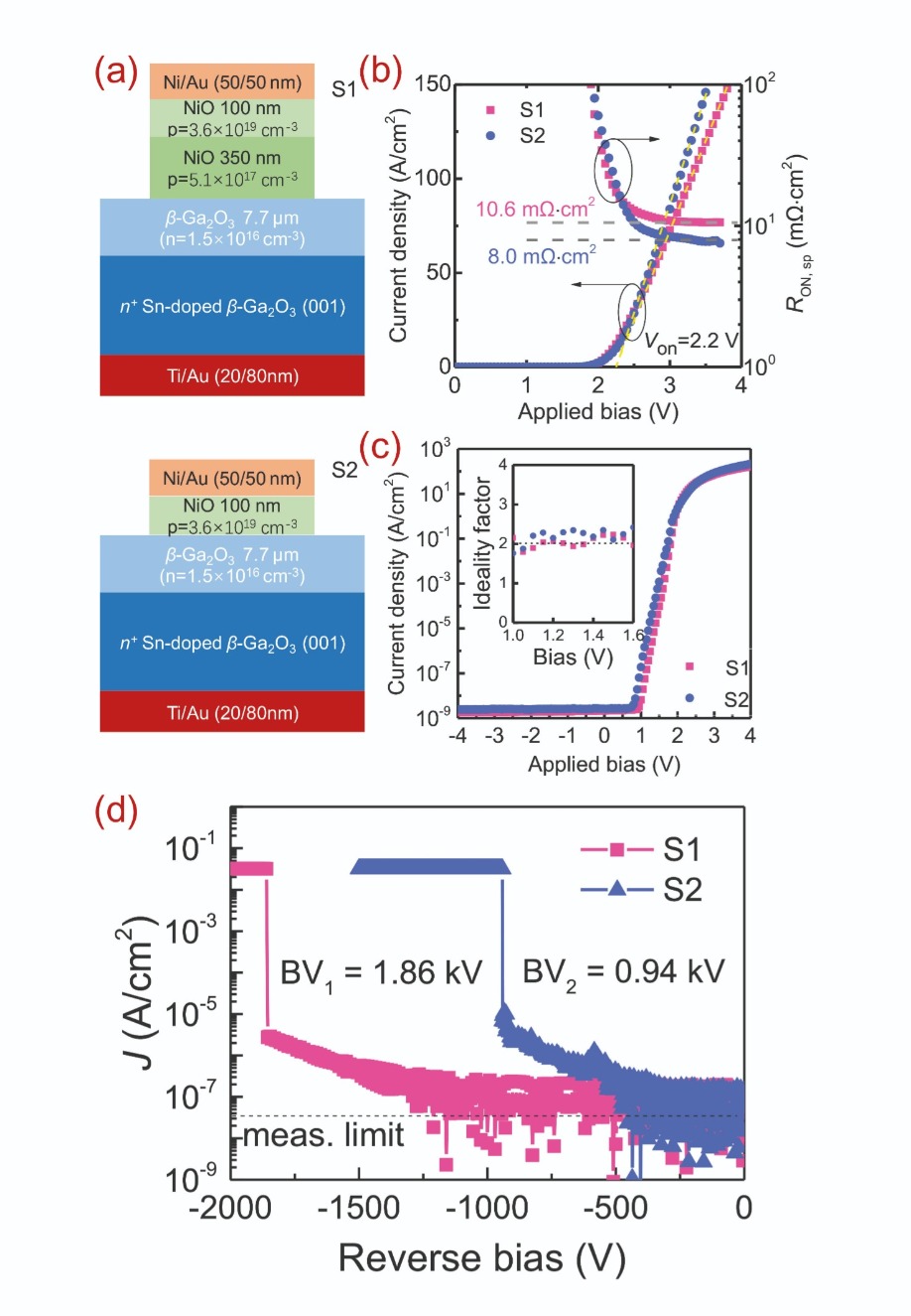
a) Cross-section of a vertical NiO/β-Ga2O3 heterojunction diode with two structural designs; (b) linear plots of current-voltage characteristics and extracted specific on-resistance as function of forward bias, with the turn-on voltage obtained by fitting the linear segment; and (c) semi-logarithmic plots of current-voltage characteristics. The inset of (c) illustrates the extracted ideality factor. (d) semi-logarithmic plots of breakdown characteristics.
H. Gong et al. Appl. Phys Let. 117 022104 (2020)

Adding a nanoscale cylindrical waveguide to a GaN VCSEL yields record-breaking output powers
Complex methods for controlling the transverse mode in blue-emitting VCSELs are holding back commercialisation of this device. But this issue can be addressed by introducing a nanoscale cylindrical waveguide, a technique recently pioneered by researchers at Stanley Electric and Meijo University.
Single- and multi-mode GaN VCSELs produced in this manner can deliver a high level of performance, making them attractive candidates for a variety of applications. Single-mode variants, which combine a circular emission profile with low divergence and high spectral purity, could be deployed in retinal scanning displays, atomic clocks and bio-sensors. And more powerful cousins with multi-mode operation could be used in colour projectors and car headlamps.
Many complex approaches have already been used to control the transverse mode in GaN VCSELs, including: silicon-diffusion confinement; the insertion of photoelectrochemically etched air-gap structures; the addition of either a monolithic curved structure or a Nb2O5 convex structure; and the construction of a tunnel-junction intercavity contact.
The team from Stanley Electric and Meijo University have previously added to this list with the formation of a buried lateral waveguide. It was created by dry-etching p-type GaN, before depositing SiO2 with a self-aligned process. A high-performance VCSEL resulted, which used the insulating oxide for optical confinement, but not lateral current confinement.
Building on this development, the team are now using reactive-ion etching to create even better VCSELs. They feature a GaN cylindrical waveguide with a step height of just 5 nm that provides current and optical confinement.
Spokesman for the team, Masaru Kuramoto from Stanley Electric, points out that reports in other papers show that dry-etching using chlorine-based gases causes compensation of acceptors in p-type GaN surfaces, due to the generation of nitrogen vacancies. This degrades rectifying quality and limits the formation of p-type ohmic contacts.
“Based on these studies, it is expected that a newly designed structure, using chlorine-based reactive-ion etching plasma treatment, can also be employed to achieve current confinement.”
To produce VCSELs, the team loaded a GaN substrate into an MOCVD reactor and deposited a 40-pair AlInN/GaN distributed Bragg reflector and a cavity containing five 3 nm-thick InGaN quantum wells. Chlorine-based reactive-ion etching defined a 5 nm-high cylindrical waveguide, before addition of an indium tin oxide layer, followed by a top mirror formed of 10.5 pairs of SiO2 and Nb2O5, completed device fabrication.
Measuring the near-field profile of this VCSEL, operating below threshold, revealed a homogeneous emission pattern across the aperture, which is defined by the waveguide. This finding indicates the high degree of optical and current confinement within the VCSEL.
Operating at 20 °C, devices with a 7 μm-diameter cylindrical waveguide produced a continuous-wave output power of 23.7 mW, a maximum slope efficiency of 1.2 W A-1, and an external differential quantum efficiency of 43.6 percent. Operating temperature for these 450 nm lasers could reach 140 °C. According to the team, all these values break new ground.
The researchers also produced a variant with a smaller waveguide, delivering single-mode emission. Using a diameter of just 3.3 μm, this VCSEL, which emits at the slightly shorter wavelength of 442 nm, produced a continuous-wave output power of 7 mW, a maximum slope efficiency of 0.7 W A-1 and an external differential quantum efficiency of 25 percent.
One of the goals for this team is to further improve the efficiency of their GaN-based VCSELs. “They are still relatively low in comparison with GaAs-based VCSELs and GaN-based edge-emitting laser diodes,” says Kuramoto.
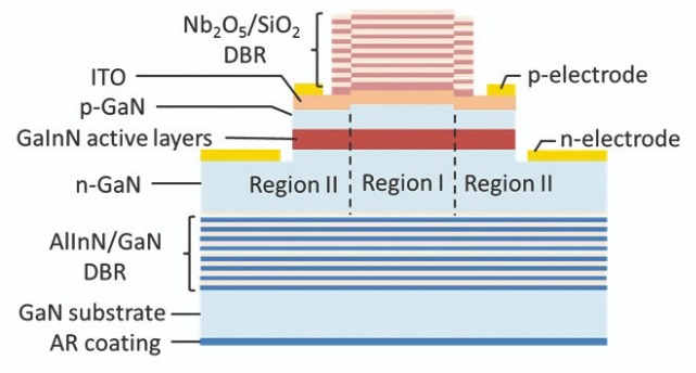
A cylindrical waveguide with a height of just 5 nm provides lateral confinement for the current and optical modes.
M. Kuramoto et al. Appl. Phys. Express 13 082005 (2020)

Oxide vapour phase epitaxy enables an incredibly low on-resistance in GaN p-n diodes
A team from Japan has produced vertical GaN p-n diodes with an on-resistance of just 0.08 mΩ cm2.
“The on-resistance is a record for gallium nitride, and lower than values for gallium oxide, as far as I know,” says team spokesman Junichi Takino, who is affiliated to Panasonic Corporation and Osaka University.
The key to this incredibly low on-resistance is a high-quality substrate produced by oxide vapour phase epitaxy (OVPE). Substrates have a dislocation density of 8.8. x 104 cm-2 and a resistivity of just 7.8 x 10⁻⁴ Ω cm.
Takino believes that the technique used to make these substrates is compatible with high-volume manufacturing. The OVPE method does not generate solid by-products and reactor maintenance is easy. What’s more, this growth technology produces GaN wafers with far simpler apparatus than that associated with HVPE, the mainstream method for GaN wafer manufacturing.
The team from Panasonic, Osaka University and Hosei University produced their high-quality material by loading a free-standing, HVPE-grown GaN seed wafer into a growth chamber and introducing ammonia and Ga2O gas, which is generated by reacting gallium metal with H2O gas. Hydrogen and nitrogen act as carrier gases.
Using temperatures in the growth and source zones of 1200 °C and 1130 °C, respectively, 500 μm-thick films were produced using a growth rate of 60 μm/hour. Following substrate removal, polishing yielded high-quality free-standing wafers (see Figure 1).
Given the growth conditions, it’s not surprising that the GaN substrate is heavily doped with oxygen. However, this did not lead to cracks, dislocations and unwanted doping in an MOCVD-grown GaN epilayer, due to lattice mismatch and diffusion of oxygen.
Diodes were produced on OVPE-grown GaN substrates, and, to provide a control, also on HVPE-grown substrates. After growth of the epistructures (shown in Figure 2), dry etching defined mesa structures. Depositing a spin-on glass and SiO2 film added an anode and cathode, completing device fabrication.
Measurements on the p-n diodes revealed that the device produced on OVPE-grown GaN had a current density of just 10-4 A cm-2 up to 1.8 kV. For the control, the breakdown voltage is slightly lower for reasons still under investigation.
Driven at 4.5 V, the diode on the OVPE-grown GaN substrate had an on-resistance of just 0.08 mΩ cm2, compared with 0.68 mΩ cm2 for the control. Enhanced conductivity modulation is thought to account for this dramatic difference.
Goals for the team are to produce 6-inch wafers with their growth technology, and demonstrate diodes and transistors capable of handling 100 A or more.
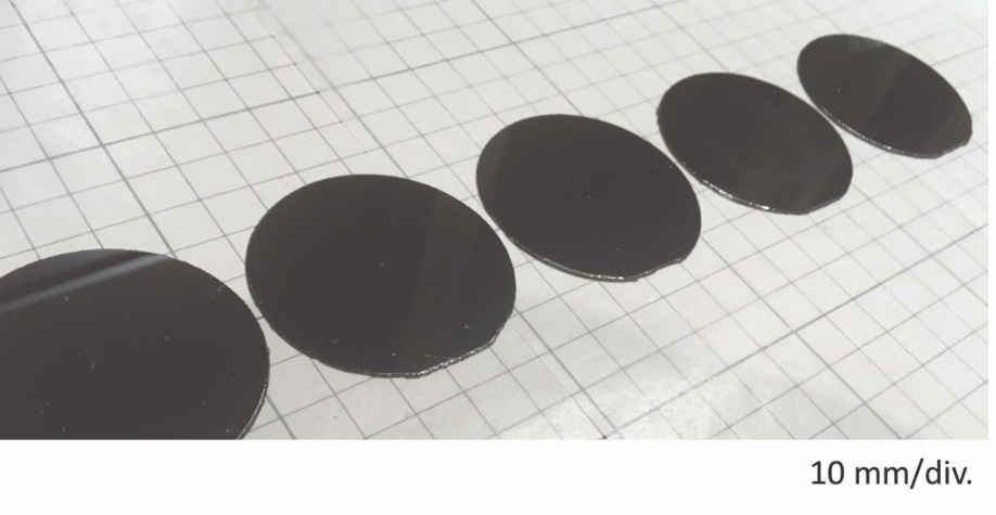
Figure 1. OVPE produces freestanding 2-inch GaN substrates with very low defect densities.
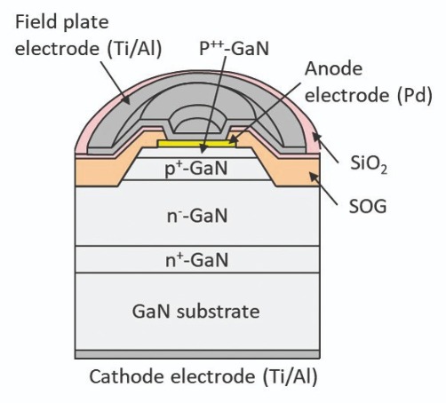
Figure 2. The diode contains: a 2 μm-thick GaN buffer layer; 13 μm-thick and 0.5 μm-thick GaN layers doped with silicon to a concentrations of 2 x 1018 cm-3 and 1 x 1016 cm-3, respectively; and GaN layers, with thicknesses of 0.5 μm and 30 nm, magnesium-doped to concentrations of 1 x 1018 cm-3 and 2 x 1020 cm-3, respectively.
J. Takino et al. Appl. Phys. Express 13 0710101 (2020)
