


IN THE JUNE EDITION of Compound Semiconductor, I always take a look at changes in the share prices of leading companies in our industry.
As I embarked on the task this year, I had a sense of dread. I knew that while the most devasting impact of the Covid-19 pandemic had been the loss of hundreds and thousands of lives, a heavy toll had been inflicted on the economy. Millions of jobs have disappeared, and there have been unprecedented falls in the price of numerous shares.
But not all shares have fallen far – and some have made a great recovery. In general, tech stocks tend to have fared well, and as is the case in many years, if you had backed the right firms within our industry, your portfolio will have gained in value – and if you had backed the wrong horses, you would be out of pocket.
Maybe the relative success of our industry is not as surprising as it first appears. For starters, many chipmakers have not had to shut their fabs, because governments deem them as an essential activity. And the devices they are churning out are being deployed in products in high demand that are needed to get us all through the crisis.
Take Lumentum, for example, occupying second spot on this year’s Share Price Leaderboard. The impact of Covid-19 on its business has been well documented in a candid conference call on 5 May discussing third fiscal quarter earnings. During that call company CEO Alan Lowe revealed that while revenues took only a relatively small hit in the third quarter, they will take a far bigger one in the fourth. Note that this admission did not spook the markets, which must believe that Lowe is handling this crisis well. Instead, the company’s valuation went up a few percent.
Lumentum is a multi-national, running wafer fabs on three continents, and the spread of the pandemic has exacerbated the challenge. Issues were first felt at the manufacturing facility in Shenzhen, China, which struggled after Chinese New Year, due to difficulties in obtaining supplies from third-parties. While this situation is now improving, the facility in Malaysia is only just starting to recover after a three week shut down and fabs in the US, the UK and Japan are not at operating at full throttle, due to the social distancing measures.
Many companies will be experiencing similar problems to those of Lumentum. Let’s be under no illusion that the coming months will be tough, but with our fabs still running, we are in a far better position than that facing many other sectors.
Micro-LEDs could become a mainstream technology for displays of all sizes, according to IDTechEx, which outlines the challenges and opportunities in a new report MicroLED Displays 2020-2030: Technology, Commercialisation, Opportunity, Market and Players.
Display markets today are dominated by LCDs, whose manufacturing is shifting to China for cost reasons. OLED technology is used in premium displays and is dominated by South Korean firms. MicroLEDs open up some new opportunities, says IDTechEx. They offer a wide colour gamut, high luminance, low power consumption, excellent stability and long lifetime, wide view angle, high dynamic range, high contrast, fast refresh rate, transparency, seamless connection, and sensor integration capability.
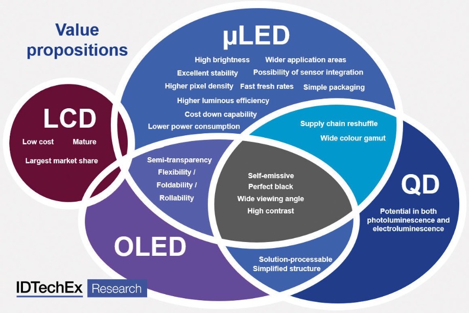
An increasing number of MicroLED prototypes have already been displayed to the public, but there are still engineering and manufacturing issues to overcome. For instance, conventional LEDs can reach external quantum efficiencies as high as 70 percent, while tiny microLEDs less than 10 μm in size may struggle to reach 20 percent. Red LEDs are especially challenging, with low efficiencies and brittle features. Tiny microLEDs have large surface areas, which may lead to more defects during the fabrication process.
Solving engineering/manufacturing challenges is important, including die size miniaturisation while maintaining the high efficiency, chip design and chip manufacturing technique improvement.
There are many steps and processes to fabricate a microLED display, with varied difficulties. In earlier years, the major focuses of research and development were on die miniaturisation, chip design, efficiency enhancement, mass transfer and full colour realisation.
Recently, more and more players realise a complete understanding of all of the processes is the key. Therefore, an increasing number of firms have put more efforts into technologies such as inspection, repair, driving, image improvement, light management and high-volume production equipment.
Involving multiple existing industries and new industries, micoLED displays may re-shape the existing LED and display supply chain, resulting in a lengthy and complex new one. New technology approaches and new products can also provide new opportunities for the players, such as the CMOS industry taking a position in the microLED-based micro-display supply chain.
Each player will optimise their gain in the value chain, and therefore, a deep understanding of the technology and market status is important.
Luminus Devices, a US start-up that uses technology originated from Massachusetts Institute of Technology (MIT), has announced the availability of its newest UVC LED, the XBT-3535, with performance ranging from 50 mW to
80 mW in the 275-285 nm range.
According to the company, the price-performance combination of the XBT-3535 will allow companies to quickly bring novel and affordable disinfection and sterilisation solutions to market.
The germicidal effectiveness of UVC LEDs against E-coli, MRSA and a variety of pathogens has been well documented. UVC LEDs with wavelengths shorter than 280 nm are shown to be as or more effective than mercury lamps for disinfection and sterilisation. However, performance, cost, and lifetime have been, in some combination, the factors slowing adoption of UVC LEDs.
“Luminus’ mission is to improve people’s health and wellness by making LED-based disinfection technology universally affordable in healthcare, water- and air-purification applications,” said Murali Kumar, director of specialty marketing.
“Our latest devices, like the new XBT-3535 from Luminus, now have median lifetimes well in excess of 10,000 hours at nominal operating conditions, their increased power output minimises the number of LEDs required in a system, and pricing in volume has been reduced to a level below $0.10/mW. The convergence of these three factors makes the large-scale deployment of UVC LEDs practical and accelerates the phase-out of lamps containing harmful substances such as mercury.”
According to a new report by Global Market Insights, the market valuation of infrared LEDs will cross $1 billion and shipments cross 8 billion units by 2026.
IR LEDs of wavelength 700 nm – 850 nm are likely to witness the strongest growth over the forecast period owing to their increasing applications in medical treatment appliances and IR illumination in solid-state lasers.
Favourable government regulations to mandate the use of IR lighting to ensure driver safety will add an opportunity for market growth.
This has led to manufacturers investing in interior and exterior lighting applications, such as night vision lighting systems, head-up displays, and front lighting with active bending features, driving the demand for IR LEDs.
The rising demand for a strong surveillance system worldwide is also likely to boost IR LED market growth over the coming years. The integration of disruptive technologies with surveillance systems, such as smart sensors and IoT, to improve the performance will add an opportunity for market growth. These systems are experiencing high adoption from military applications, smart cities, industries, among others.
The 950 nm –1020 nm segment held a market share of over 5 percent in 2019 and is likely to grow at a CAGR of
5 percent over the forecast period, according to the report.
These high-wavelength devices are used for light sources for remote controller, infrared communications, and photo couplers. This will increase their adoption in applications such as surveillance cameras, sensors for factory automation, infrared range finders for digital cameras, and smoke detectors.
Imaging applications are anticipated to register a CAGR of over 7 percent over the forecast period.
IR LEDs for image processing are used in a wide range of applications such as defence & security, medicine, industrial, and handheld mobile devices.
Global smartphone shipments dropped by 16.8 percent in the first quarter as vendors struggled to manage coronavirus-driven production shutdowns, product-launch delays and depressed consumer demand.
Shipments in the first quarter fell to 274.4 million units, down from 329.9 million during the same period in 2019, according to the Omdia Smartphone Intelligence Service. This plunge impacted all the major smartphone brands, with nine of the top-10 OEMs suffering shipment declines compared to the first quarter of 2019.
“Early in the first quarter, the smartphone market was sent reeling by the shutdown of production at facilities in China, which halted the manufacturing of phones and their key components,” said Jusy Hong, smartphone research and analysis director at Omdia.
“While concerns about this situation have been alleviated, the smartphone brands also faced new challenges, including disrupted launch schedules for new phones. Even more troubling for smartphone makers is a major decline in global demand due to government lockdown mandates.”
Despite expected rebounds in some countries, the rest of the year is expected to be challenging for smartphone OEMs. Omdia forecasts global smartphone shipments will decline to 1.20 billion units this year, down 13.1 percent from 1.39 billion in 2019.
Almost across the board, smartphone OEMs faced significant declines in unit shipments compared to the first quarter of 2019.
Samsung retained the top position, with 58.9 million units shipped during the first quarter – a 17 percent decline compared to the first quarter of 2019.
Second-ranked Huawei saw its shipments decline by more than 17 percent, to 49 million units, down from 59.1 million in the first quarter of 2019. Apple, in third place, saw shipments decline to 38.5 million units, down from 43.8 million a year earlier. The 12.0 percent decline comes during the first quarter, historically the weakest period of the year for Apple.
Rounding out the Top 5 are Xiaomi and Oppo. Out of the Top 10, Xiaomi experienced the second least severe decline in the quarter, of 8.2 percent. Only Tecno, in 10th place, attained a lower decrease with a 7.6 percent year-over-year decline. Xiaomi shipped 25.3 million units in the first quarter, compared to 27.5 million units in 2019. Oppo, on the other hand, suffered a 19.2 percent decline, with shipments falling to 20.4 million units, down from 25.2 million a year earlier.
The rest of the Top 10 is made up of vivo, Realme, Motorola, LG, and Tecno. The bright spot here is Realme, which achieved year-over-year growth based on its continued success in India. Seventh-ranked Realme was the only top-10 OEM to attain growth during the quarter, with shipments totaling 6.1 million units, up 88 percent from 3.2 million during the first quarter of 2019.
For the others in this group, the first quarter brought significant challenges. Looking at vivo, company shipments declined 19.9 percent, falling from 24.3 million units last year to 19.5 million this year. Motorola, in eighth place, saw shipments decline 35.4 percent to 5.5 million units. While Motorola finally launched its updated RAZR, featuring a foldable display, the publicity surrounding that high-profile device was not enough to support the overall performance of Motorola’s product portfolio.
With or without the impact of the pandemic, LG continues to struggle with its mobile handset division. Shipments declined to 5.4 million units, down from 8.6 million units a year ago – a drop of 37.4 percent. Rounding out the top 10 is Tecno, which saw units decline by a relatively modest 7.6 percent, declining from 3.8 million units last year to 3.5 million units in the first quarter.
“The smartphone market will face major struggles in the first half of 2020 as different countries experience the initial shock and recovery periods at different times. That’s why OEMs are more afraid of second-quarter sales results,” Hong said. “However, Omdia does expect the smartphone market to start to recover in some countries and regions in the second half of the year.”
Early in the first quarter, the most severe impact on the smartphone market was the shutdown of production and supply chain facilities in China. However, fears over a prolonged closure of essential production, supply chain and logistics operations in China have been alleviated, as signs point to economic activity ramping up quickly in the country.
Smartphone makers in the first quarter also had their product-launch plans disrupted by the cancellation of the Mobile World Congress event in Barcelona, Spain, where many companies had planned to roll out new products.
“Because of the cancellation of the Mobile World Congress, and uncertainty in the supply chain, original product schedules had to be re-evaluated,” said Gerrit Schneemann, senior analyst, smartphones, at Omdia. “However, OEMs seem to have found their footing on how to address new device launches going forward.”
The impact of the outbreak on the smartphone business has now shifted almost completely to the demand side of the equation.
“Although handsets can be produced at nearly normal levels, the markets for these handsets are mostly in some state of shutdown,” Hong said. “Some countries have made more progress in dealing with the outbreak, while others are still in the midst of fighting the pandemic, and still others won’t feel the full effects of the pandemic until later in the year.”
In Europe, where some countries have been under strict lockdown rules for some time, initial efforts have been made to ease restrictions.
Power Integrations has announced that its InnoSwitch3-MX isolated switcher IC family has been expanded with the addition of three new PowiGaN devices.
As part of a chipset with Power Integrations’ InnoMux controller IC, the new switcher ICs now support display and appliance power supply applications with a continuous output power of up to 75 W without a heatsink.
The InnoMux chipset employs a single-stage power architecture that reduces losses in display applications by
50 percent when compared with conventional designs, increasing overall efficiency to 91 percent in constant-voltage and constant-current LED backlight driver designs.
Additionally, by eliminating the need for post regulation (i.e. buck and boost) stages, TV and monitor designers can halve component count, improving reliability and reducing manufacturing cost.
With a high breakdown voltage of 750 V, the PowiGaN InnoSwitch3-MX parts are also extremely robust and highly-resistant to the line surges and swells commonly-seen in regions with unstable mains voltages.
InnoSwitch3-MX flyback switcher ICs combine the primary switch, the primary-side controller, a secondary-side synchronous rectification controller, and PI’s innovative FluxLink high-speed communications link.
The InnoSwitch3-MX receives control instructions from its chipset partner InnoMux IC, which independently measures the load requirements of each output and directs the switcher IC to deliver the right amount of power to each output, maintaining accurate regulation of current or voltage.
“By using our PowiGaN technology we are able to address higher-output applications in TVs, monitors and appliances that employ LED displays. The chipset increases efficiency beyond the requirements of all mandatory regulations and improves manufacturers’ scores in EU efficiency labeling programs,” said Power Integrations’ product marketing manager Edward Ong.
MKS Instruments has announced the Ophir FluxGage 604 compact measurement system for LED luminaires.
This new series features four additional colour sensors evenly arranged in the bottom of the device delivering further x,y, and CCT data as well as the illuminance.
Within seconds the user gets an overview of the colour and overall uniformity of the measured light, according to MKS. This allows direct evaluation of LED chips or optical assemblies used for colour mixing and beam shaping within the design process in order to find the optics that provide the optimal light for a particular application.
The system can also be used in end-of-line LED luminaire production applications to instantly detect issues, ensuring high-quality product standards are met. The Ophir FluxGage measurement system also measures total luminous flux, colour parameters and flicker.
“Knowing the uniformity of light is important in a wide variety of applications, such as lighting in industrial, educational, or medical facilities; offices; TV studios; as well as streets, parks, and other urban spaces,” said Simon Rankel, business development manager LED for the Ophir brand.
“Historically, it has been challenging to measure the colour uniformity of LED luminaires as measurement devices like goniometers deliver a detailed analysis but are large, relatively slow, and expensive.”
“Ophir FluxGage 604 measurement system revolutionizes the testing of LED luminaires as the compact system only needs a space the size of the luminaire being tested, which makes handling easy. In addition, measurements can be performed in less than two seconds and literally in any environment.”
Ophir FluxGage 604 measurement system features smart tristimulus (RGB) colour sensors that boost the measurement system’s capabilities, making it suitable for fast testing, both in R&D and for quality control in a production environment. All photometric measurements are performed in 2p geometry, thus the colour distribution of LED assemblies and luminaries can easily be evaluated with the FluxGage system.
In addition, the new colour-sensor functionality enables useful comparisons of the colour-mixing performance of LED lenses, reflectors, diffusers, and homogenisers without the need for an expensive goniometer.
As the total luminous flux of the different LED luminaires can vary significantly depending on its application, Ophir FluxGage 604 measurement system is available in two sensitivities to deliver precise measurements.
The standard FluxGage 604 measurement system measures LED luminaires in a luminous flux range between 500 and 40,000 lumens. The high-sensitivity FluxGage 604/100LM measurement system covers the range between 100 and 5,000 lumens. Both versions include four sensors to measure colour uniformity.
All FluxGage systems are based on technology that uses solar panels as light detectors. The panels are arranged on the inside walls of the measurement cavity and are covered with a special black layer with hundreds of transparent pinholes, creating the effect of many tiny radiometers.
MKS says that the design significantly reduces the reflectance of the solar panels, creating a measurement system resembling a goniophotometer in a dark room.
Unlike an integrating sphere, the FluxGage system is insensitive to reflections going back and forth between the measurement device and the luminaire under test.
Luminous flux and other colour parameters are calculated based on the measurements of the integrated spectrometer; a fast photodiode is used for measuring flicker.
Integrated application software simplifies set up and operation; all of the photometric data of the light source is displayed. The FluxGage system connects to a PC via a USB cable. The Ophir FGC100, a NIST-traceable, broadband LED calibration standard, is used for periodic calibration of the FluxGage system.
Aixtron’s supervisory board has appointed Jochen Linck as a new member of the executive board with effect from December 1, 2020 or earlier in the role of chief technical and chief operating officer. At his own request, board member Bernd Schulte will retire at the expiry of his contract on March 31, 2021, and Felix Grawert will take over as chairman and CEO.
Linck’s appointment is for three years. As of April 1, 2021, he will assume responsibility at Aixtron for the areas of development, purchasing, manufacturing and logistics, quality management and IT.
Linck has many years of experience in international management functions in various areas such as development, product management or launch management. The 54-year-old most recently served on the Executive Committee of Diebold Nixdorf. a global provider of cash management and self-service machines for banking and retail.
As managing director of DN Systems, he was responsible for the development and launch of a new product generation of ATMs. Prior to this, the engineer with a PhD in lean production was a partner at McKinsey & Company, with a functional focus on product development, production and strategy in the mechanical engineering, aerospace and automotive industries.
The supervisory board considers the technology expert with many years of management experience to be the ideal person to lead Aixtron into the next growth phase together with his colleagues on the board and the entire team. In addition, the executive board is to be expanded to include a CFO, bringing the total number of members to three. The Supervisory Board’s Nomination Committee is working to soon fill this position.
Aixtron’s technologies address a number of different growth markets, for which market researchers predict double-digit annual growth rates over the next few years. Aixtron intends to benefit from this growth and, with an expanded board, sees itself well set up for the future.
Bernd Schulte has been with Aixtron since 1993 in various positions and has been a member of the board since 2002. Today, he manages the company together with Felix Grawert and intends to retire when his board contract expires in March 2021. Until then, Schulte will be at full disposal to the Company and the board to actively support his new colleagues.
Kim Schindelhauer, chairman of the Supervisory Board of Aixtron SE comments: “We would like to express our special thanks to Bernd Schulte, who has accompanied and successfully led Aixtron for more than 28 years at the time of his retirement. Schulte has shaped Aixtron with his deep understanding of technology, close customer relationships and entrepreneurial drive, and has made a significant contribution to the company’s success. On behalf of the Supervisory Board, I would like to thank Schulte for his many years of successful service to the company. The Supervisory Board wishes him all the best for his personal future”.
“The generational change in the Aixtron Group’s leadership has started with the appointment of Felix Grawert in 2017. The appointment of Jochen Linck and the soon to be appointed CFO, will then complete the generational change. With this management team, the company is excellently positioned for future growth,” explains Kim Schindelhauer.
Osram Opto Semiconductors has announced a new family of LEDs called Synios S 2222, suitable for a wide range of applications: from customised lighting solutions for electronic devices, ambient lighting for trains and planes to high-quality architectural lighting.
The product family has compact dimensions, combined with very good brightness values and the ability to cover the entire colour palette.
Osram says the new family provides an efficient and flexible platform for a variety of low- and mid-power applications, and spans 10 mA to 200 mA. Customers can choose from six colours and combine them to create more. In addition to white versions (3000 – 6500 K, CRI >80), the product family includes versions in blue (445 nm – 460 nm), green (520 nm – 540 nm), yellow (583 nm – 595 nm, conversion and direct emission), red (612 nm –
626 nm) and deep red (626 nm – 636 nm).
The family’s uniform dimensions of 2.2 mm x 2.2 mm and solder pad design make it particularly easy to integrate into many different solutions. The low package height of only 0.6 mm makes extremely flat lighting solutions possible.
Osram is responding to the trend of producing ever smaller discrete components with the highest possible performance.

For example, the yellow converted variant delivers an outstanding brightness value of 50 lumen at 140 mA. Depending on the application, additional optics can be easily applied to the respective component due to the centric chip position in the package.
“With the Synios S 2222 product family, we offer our customers compact, high-quality LEDs to help them easily realise individualised lighting solutions. “
“Thanks to the special package design, the products are easy to handle via pick and place in series production,” explains Alvaro Wulff, Product Manager for Illumination at Osram Opto Semiconductors.
“Depending on the application, customers can choose from a wide range of colours while benefiting from our latest chip and package technologies.”
With a heavy dependence on cellular terminals, recent forecasts of declining handset shipments in response to the Covid-19 pandemic will result in lower GaAs device revenue in 2020. This is a conclusion of the Strategy Analytics Advanced Semiconductor Application (ASA) insight A First Look at the Effects of COVID-19 on GaAs Revenue.
Based on current trends in several application segments, the insight forecasts a likely trajectory for GaAs revenue out to 2025.
“GaAs RF device revenue growth has struggled in recent years and revenue actually declined for the first time in many years in 2019,” noted Eric Higham Director of the Advanced Semiconductor Applications (ASA) service. “GaAs revenue links closely to trends in the cellular segment, so recent forecasts of sharp drops in smartphone shipments caused by the Covid-19 pandemic will contribute to further declines in GaAs revenue.”
He went on to say, “The complete effects of Covid-19 on the supply chain remain unclear, but I’m optimistic about the future of GaAs device revenue. Based on the most recent information, 5G will become a strong growth engine and GaAs device revenue should be reaching new highs in the next few years.”
SweGaN AB, a manufacturer of custom-made GaN-on-SiC epitaxial wafers based on a unique epitaxial growth technology for RF and power components and devices has announced a new benchmark for GaN high-frequency devices based on SweGaN QuanFINE material. The demonstration promises commercial benefits for the entire GaN RF value chains including telecom, space, and military markets.
In a new joint study with the Chalmers University of Technology Department of Microtechnology and Nanoscience, SweGaN explored QuanFINE epitaxial wafer performance, based on GaN HEMT technology at Chalmers - Gothenburg, Sweden.
Collaborating with scientists from the university, the team performed a new benchmark comparing the conventional 1.8-μm thick iron-doped GaN buffer epi-structure to SweGaN’s ‘buffer-free’ QuanFINE GaN HEMT heterostructures for microwave applications. The study revealed that the new concept using a total GaN layer thickness of 250 nm does not compromise the material quality and device performance. Furthermore, the device results indicate that the ‘buffer-free’ QuanFINE material can outperform conventional materials at the device level in the long run.
For SweGaN customers and manufacturers, the ultimate benefits – resulting from the new ‘buffer-free’ concept, and including lower trapping, better carrier confinement and lower thermal resistance – could lead to higher device power efficiency and better reliability of GaN high-frequency devices.
Findings from the research collaboration are published in IEEE Electron Device Letters (Early Access) Microwave Performance of ‘Buffer-Free’ GaN-on-SiC High Electron Mobility Transistors by the joint research team of Ding-Yuan Chen, Anna Malmros, Mattias Thorsell, Hans Hjelmgren, Olof Kordina, Jr-Tai Chen and Niklas Rorsman.
“The new QuanFINE concept possesses many interesting features that are very attractive for both high frequency and power electronics,” says Niklas Rorsman, Research Professor at Chalmers University of Technology. “As an example, the possibility of a pure AlN back-barrier will be beneficial both for good electron confinement and thermal resistance. We at Chalmers are thrilled to be part of this development in GaN HEMT Technology.”
“Currently, GaN-on-SiC epitaxial wafers for Ka band applications are either immature or suffer from severe trade-offs,” says Jr-Tai Chen, CTO at SweGaN AB. “Our QuanFINE epiwafers are a highly feasible solution that can resolve issues our customers are dealing with regarding short-channel effects in the high-frequency devices.”
“We already have numerous product companies interested in our material as well as end users in the value chains,” continues Chen. “Four key target groups for QuanFINE epiwafers include the world’s leading foundries, IDMs (integrated device manufacturers), fabless companies, and end users, in Europe, Asia and USA. ”
Key demonstrations from the joint collaboration are:
• Physical simulations (TCAD) indicating that QuanFINE can be highly favourable for improved electron confinement.
• Pulsed-IV measurements that demonstrate a unique advantage of using the QuanFINE concept, showing a lower buffer-induced dispersion compared to the conventional thick, iron-doped buffer.
• Large signal measurements showing that the QuanFINE concept can provide highly competitive output power levels and efficiency, vastly beneficial to product companies and end users.
According to SweGaN, the beauty of the QuanFINE concept is a thin undoped GaN channel layer in between an AlGaN barrier layer and a AlN nucleation layer which acts as a sandwich-like double heterostructure – offering sufficient 2DEG confinement with much lower trapping effects as compared to conventional iron- and carbon-doped epi-structures. Moreover, the further reduction of GaN channel thickness will path a new road for small gate length devices as compared with conventional AlGaN back-barrier epi-structure, which suffers from weak thermal dissipation performance.
Further studies of the carbon impurity and the thickness of the UID GaN layer, are anticipated to continue to further improve the ‘buffer-free’ QuanFINE concept.
GaN Systems has announced the debut and availability of a new amplifier evaluation kit for high sound quality Class-D audio systems.
The evaluation kit includes a 2 channel, 200 W per channel (8 Ω) Class-D audio amplifier and companion 400 W, continuous power audio-grade SMPS. This solution highlights an easy plug and play design with features such as multi-audio signal inputs, bridge-tied load output, and open-loop/closed-loop toggling.
With GaN, the design is very efficient and operates without heatsinks. These features allow audio design engineers to create premium audio products at shorter time to market and at an affordable price.
The convergence of audio trends including demand for more power, size and weight reduction, and growing consumer demand for better audio quality requires innovative approaches to enhance sound quality, increase efficiency, and reduce size which is served by GaN power semiconductors. Applications include smart speakers to automotive and high-end home audio systems.
“Class-D Audio amplifiers are reaching a new level of performance with GaN. Industry experts and audiophiles alike have tested and listened to the output of our design and are truly impressed,” says Paul Wiener, GaN Systems’ VP of strategic marketing.
“The audio quality combined with the thermal and EMI/EMC performance provide a great solution for our customers.” Additionally, GaN Systems has published a new white paper, See, Feel, and Hear the Difference with GaN Class-D Amplifier and Companion SMPS, reviewing the GaN Systems audio evaluation kit using the standard set of industry performance and validation tests.
ZF Friedrichshafen AG, an automotive supplier, and VisIC Technologies, a maker of GaN devices for automotive high-voltage applications, has announced they will work together to create the next generation of high-performance and high-efficiency electric drivelines for vehicles.
The partnership will see the two companies deepen their development efforts, based on VisIC D3GaN semiconductors technology. The focus of the joint efforts will be on 400 V driveline applications, covering the largest segment of the electric vehicle market.
“Our partnership with ZF for the development of GaN-based power inverters in electric vehicles illustrates the break-through of GaN technology in the automotive industry,” said Tamara Baksht, CEO of VisIC.
“VisIC’s D3GaN technology was developed for the high reliability standards of the automotive industry and offers the lowest losses per Rds(on). It also simplifies the system solution and enables high-efficiency and affordable power train solutions. It is definitely the next step for the automotive electrical driveline.”

ZF’s fast adoption of semiconductor technologies such as SiC and GaN makes it a leader in the development of the most cost-effective and highly efficient electric drivelines. Through their extended R&D partnership, ZF and VisIC deepens their existing joint efforts in the application of GaN semiconductors for inverters.
Amid trying times, precursor supplier Ereztech has opened a US manufacturing facility to deliver more materials to more compound semiconductor manufacturers. Rebecca Pool investigates.
WHILE THE CORONAVIRUS PANDEMIC might be a surprising time to launch a manufacturing facility, Ereztech has done just this. In May this year, the manufacturer of organometallic precursors – critical to semiconductor thin-film deposition – opened its new R&D lab and manufacturing facility in Wisconsin, US.
The new operation adds US manufacturing capability to Ereztech’s Russia-based distribution network of precursor manufacturers and manufacturing operations. And it also allows the company to synthesize more exotic and reactive precursors based on pyrophorics and noble metals.
“Coronavirus and the subsequent economic challenges certainly add a layer of uncertainty, but we see this only as a short- to mid-term problem,” says Ereztech chief executive Roman Rytov. “This expansion brings our advanced and cost-efficient precursor development closer to our US customers, allowing for a broader product selection and accelerated development.”
“We started the process for setting up the facility back in 2019 and nobody predicted that this [pandemic] would happen but we are very positive about the future,” he adds.
Indeed, Rytov and his Ereztech colleagues are probably well-placed to deal with these uncertain times. Without a doubt, working with organometallic precursors is hardly a predictable business, with these reactive complexes often delivering surprising chemistry.


As Rytov puts it: “We’ve witnessed curious stories such as synthesising a molecule which the customer anticipated being solid and the end result was a liquid... This type of chemistry often surprises, but for us, this is normal.”
Indeed, for every ten new molecules that the company initially synthesises – to assess for stability and yield – only one will be suitable for further processing and scaling. So with this in mind, Ereztech has developed its so-called 25 grams programme, which promises at-cost synthesis of as little as 25 g of a target molecule, while protecting intellectual property for its customers.
According to Rytov, the programme allows molecule characteristics to be analysed swiftly and efficiently and can help to provide reliable and predictable pricing for larger molecule quantities.
“We believe this programme is unique amongst precursor materials manufacturers,” he says. “Due to the high risk of failure at this stage of precursor development, we decided to find out the absolute minimum viable amount of a molecule you need to synthesise, to understand how it works, and at 25 grams, this doesn’t come with a large price tag.”
And if the 25 g test batch is stable and meets purity standards, then Ereztech can refine the compound and eventually scale production to thousands of kilograms. “Customers can get 25 g of a new molecule for as little as US$1500,” says Rytov. “We’ve had tens and tens of molecules that have gone through this process... and molecules that have come out of this programme and gone into volume production with customers now make up some
50 percent of our overall business.”
For the semiconductor industry, and especially compound semiconductor players, this trial-batch method makes sense. As manufacturers become ever-more reliant on MOCVD and ALD vapour phase processing, having access to a reliable source of precursors is critical. And the slow but steady rise of ALD has also meant manufacturers can experiment with more options for volatile precursors.
During ALD, the gas precursors are typically pulsed into the reaction chamber one at a time to slowly deposit the thin film. Crucially, the release of precursors is separated by inert gas purging to avoid unwanted gas phase reactions.
As Ereztech’s chief technology officer David Roberts points out: “Separating these reaction components was a real game-changer and people have been using precursors that simply wouldn’t have even been considered back in the 1990s due to issues over contamination of the deposited material.”
“We’ve seen this explosion in precursor options that didn’t work well with CVD – many were rejected years ago, but are now coming back for ALD,” he adds.
Proliferating device types and shrinking geometries also see industry players experimenting with different thin films and epitaxial layers to achieve the finer features during deposition processes. Roberts points to the need for Group III-V channel replacements, Ta and Mn nitride sources for dimensionless copper barriers as well as high-k dielectrics for MOSFETs.
“Many manufacturers don’t want to necessarily use the usual metal-alkyl and metal-hydride ligand precursors, but want to try something a little different.” he says. “For example, we’ve seen increasing interest in gallium sources that are not alkyls... and I think people are really beginning to investigate this, particularly for nitrides.”
“We do also see a lot of work in the simple oxides; it’s amazing the utility of that kind of thin film, and sometimes it’s difficult to tell what manufacturers are using that for,” he adds.
Critically for Ereztech, the company will now be able to synthesize these more weird and wonderful, and reactive, precursors in its US facility. According to Roberts, importing such materials from Russia to the US had sometimes proven problematic; air travel wasn’t an option while shipment via sea was time-consuming.
Instead, the company can now manufacture more and more of these up and coming precursors in the US. Case in point is diethyl zinc, increasingly used to produce highly conductive and transparent ZnO layers for transparent electrodes in thin-film solar cells, piezoelectric sensors, transistors and more.
“This is a mainstay precursor in compound semiconductors and as we dig deeper into our new US capability, we can start to make more reactive materials such as this, that were difficult to bring into the country before,” says Roberts.
And as Rytov adds: “We are already making diethyl zinc, dimethyl zinc, pyrophorics and other products in the US... we’re also expanding our product line with a few noble metal precursors, while duplicating some of our Russia-made qualified products.”
Still, few would disagree that the opening of Ereztech’s new US lab in Wisconsin can’t be the easiest of endeavours right now. Covid-19 complications have shuttered many businesses, with the need for workplace sanitation, absences and limits to face-to-face interactions complicating operations worldwide.
However, Rytov isn’t fazed. “We are still working with our industrial partners – activities are slower, but we haven’t got any cancelled projects,” he says.
“Before this, industry forecasts had been so optimistic and positive, and we’d been dreaming about opening a US facility for years,” he adds. “So we will bite the bullet and pull through... we see lots of opportunities in the compound semiconductor space – these are interesting times.”

Ereztech is serving up precursor R&D, synthesis and volume manufacturing from its new US facilities.
Thanks to the promise of substrate manufacturing costs that are comparable to sapphire and an ultra-wide bandgap that aids performance, gallium oxide power devices have the potential to displace those made from SiC and GaN by delivering a better bang-per-buck, argues National Energy Renewable Laboratory’s Senior Engineer and Analyst Samantha Reese and Scientist, Andriy Zakutayev.
INTERVIEW BY RICHARD STEVENSON
Q: When we look at wide bandgap materials for power electronics, there are the middleweights – silicon carbide and gallium nitride, which are today’s success stories – and the ultra-wide bandgap heavyweights gallium oxide, diamond and aluminium nitride. Do you think aluminium nitride and diamond can have any success?
SR: I definitely don’t expect diamond to have much of an impact, due to its high cost. However, maybe these devices could be used on satellites, where cost is far less of an issue.
My impression from attending the recent SPIE Photonics West conferences is that AlN has some technical challenges, so I’m not sure it will be a success in power electronics, but it may be useful for optoelectronics.
Q: Do you see gallium oxide as a competitor to gallium nitride? Or to silicon carbide? Or both?
SR: I think gallium oxide can take on both, as we could get devices with a low cost. Gallium oxide could easily take on silicon carbide, due to this. Gallium nitride, which is behind silicon carbide in terms of commercialisation, operates at lower voltages, and is lower in cost. But if gallium oxide gets to market quickly, it could thwart gallium nitride before it is established.
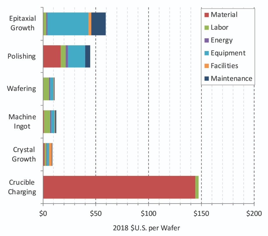
Figure 1. Ga2O3 wafer manufacturing cost by step
SR: The cost of the device depends on the cost of the wafer. Silicon carbide is a hard material, requires expensive material for wafer production, such as diamond-based polishing slurries, thus it is expensive to make. Producing gallium oxide boules is very similar to producing those of sapphire, which is used to make LEDs. So gallium oxide promises low cost.
AZ: The bulk single crystal growth from melt also has other advantages compared to chemical processes that are not directly captured in substrate cost but may impact device cost – for example, a lower defect density of the wafer, and better yield for subsequent device fabrication.
Q: Do you view the wide bandgap as the greatest strength of gallium oxide?
AZ: The biggest merit in my opinion is the availability of large-size, high-quality, electrically-dopable bulk single crystal substrates with projected low cost. This is qualitatively different from silicon carbide and gallium nitride, or aluminium nitride and diamond; the width of the band gap is only a quantitative difference.
SR: Its other strength is its ability to work at high temperatures. This is useful for making sensors that go down deep wells. It could be used by the oil industry, which needs medium-voltage devices.
Q: One of the weaknesses of gallium oxide is its low thermal conductivity. Could that be a show stopper?
SR: That depends on who you talk to. Gallium oxide devices can be very small and thin, so you can use very effective thermal management, even though the thermal conductivity is so low.
At the recent IEEE Workshop on Wide Bandgap Power Devices and Applications, a paper given by a colleague of mine – Paul Paret from NREL in Golden, Colorado – showed thermal modelling of gallium oxide devices attached to a base plate. Because the base plate can be so large compared with the size of the device, there was no impact associated with the low thermal conductivity.
AZ: In real-world power electronics systems, the overall thermal resistance is often limited not by the thermal conductivity of the substrate, but by the thermal resistance of various interfaces between the semiconductor chip and other components. So low thermal conductivity of gallium oxide may be not as big a problem as often perceived. Also it depends on the use – power electronics versus RF devices versus a myriad of other potential applications – and some are more sensitive to this problem than others.
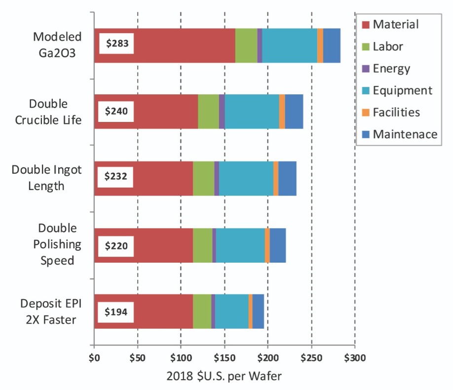
Figure 2. Ga2O3 Wafer Manufacturing Potential Cost Reduction Pathway
AZ: It is an issue for traditional device designs, but also an opportunity for creating thinking. For example, enhancement-mode – that is, normally-off – gallium oxide vertical transistors with breakdown voltage of more than a kilovolt have been demonstrated without p-type doping, using a FinFET-like structure, by a team led by researchers at Cornell.
Q: You have modelled the costs associated with producing gallium oxide devices. Tell me about the assumptions you make, and how they are justified.
SR: I modelled the cost of the gallium oxide wafer with an epilayer, and stopped at the wafer level. However, I think that the cost of making a device from a wafer could be similar for gallium oxide and silicon carbide.
The cost of producing gallium oxide is dominated by the iridium crucible. We have been very conservative in calculating this cost, assigning the number of times that it could be re-used to sources that were credible. We are confident that that it can be re-used ten times, however there were anecdotal references in literature that it could be re-used considerably more or refurbished without significant cost.
We have assumed that all the equipment for making the wafers has had to be bought new, and that there are no subsidies for the manufacturer. We also assume that the equipment is running all the time, apart from downtime for maintenance. Obviously, if you only make one or two gallium oxide wafers per month, it is going to be prohibitively expensive.
Another assumption that we made is that the gallium oxide wafers are 6-inch. Today they are commercially available in 2-inch or 4-inch, and 6-inch are in a development process, but we have used 6-inch in our modelling because we want an apples-to-apples comparison with the published silicon carbide cost.
Q: What were your key findings, in terms of wafer costs?
SR: Our figures are based on current material quotes for gallium oxide powder. If production took off, costs could come down, as there is not much of a market for gallium oxide powder today. With the stated assumptions, we find that the cost of gallium oxide is three times lower than silicon carbide, and with improvements could be five times less expensive. Additionally, gallium oxide wafer manufacturing could benefit from the expertise already gained in manufacturing of sapphire wafers.
Q: Why are the iridium crucibles so expensive?
SR: Iridium is a rare and expensive material. It’s not due to high processing costs for producing the crucible.
Q: Your work shows that the cost of a 6-inch gallium oxide wafer could be just under $300 – that’s a third of that for silicon carbide. That’s very encouraging. And you think it could be even lower than that. What are the most promising routes for getting the costs right down, and how big an impact could they have?
SR: The cost of the indium crucible could come down by 15 percent. If the size of the ingot were to double, this would provide an additional 3 percent saving. If the processing rate were to increase by 60 percent, then this could trim another 4 percent. A doubling of the growth rate could cut another 9 percent. If you put that all together, the cost of the wafer could come down from $300 to $200, a 33 percent reduction.
After that, replacing iridium with another metal would be the most promising transformative route.
Q: Novel Crystal Technology, a joint venture by Tamura Corporation and the National Institute of Information and Communications Technology, is producing gallium oxide material by two different methods. How do you think your findings relate to Novel Crystal’s production costs? Could there be differences due to economies of scale, and the maturity of the production process?
SR: I can’t comment on Novel Crystal Technology or other specific companies. However, at a conference one gallium oxide substrate maker indicated that their internal costs of production are very similar to those of our model, when they make the same assumptions. This is the best validation of our work we can get.
When companies produce just a few wafer per month, the manufacturing costs will be higher. But when you scale to volume, the costs will come down.
Q: Does a lower wafer cost directly translate into a lower bill-of-materials for a device?
SR: It is not a one-to-one scenario. There are other ‘fixed costs’. For about a three-fold reduction in the cost of the epi-wafer, the device would be about half as expensive, since the wafer is usually 60-to-70 percent of the cost of the device.
With wide bandgap devices, whether they are silicon carbide or gallium oxide, they can produce cost reductions at the system level, thanks to a reduction in the cost of the magnetics.
There is also an increase in the efficiency. Take a 50 kilowatt inverter, for example. Turning to gallium oxide devices might provide a 5 or 6 percent increase in efficiency, leading to a 2 percent increase in the electrical output from a solar farm, so an increase in revenue.
Q: Which company’s do you think will bring the first devices to market? Flosfia of Japan?
AZ: Our SPIE and Joule papers are about β-gallium oxide, which has a monoclinic structure. Flosfia is working on a-gallium oxide, which has a hexagonal ‘corundum’ structure that is similar to sapphire. That is a completely different technology. It’s not clear yet which company would emerge as a leader in β-gallium oxide devices.
Q: With silicon carbide, it took more than a decade to follow up the launch of the first Schottky barrier diode with the first MOSFET. With gallium oxide, do you expect diodes to launch first, followed by MOSFETs? And could the gap between them be a decade or more?
SR: I think it will probably be diodes first, but the wait for MOSFETs will be shorter than it has been for silicon carbide. That’s because silicon carbide has helped to pave the way for the commercialisation of gallium oxide. For example, contact layer sintering processes have been established, and there are high-temperature modules that gallium oxide devices can be designed into. The US Air Force Laboratory is very excited about gallium oxide. And if you look at the number of papers published in total, you can see that there is major interest in gallium oxide worldwide.
AZ: I agree that it is likely that gallium oxide Schottky barrier diodes will be commercialised first, because their fabrication technology is relatively straightforward. However, lateral radio-frequency transistors similar to gallium nitride may be commercialized sooner than vertical power transistors similar to silicon carbide.
SR: I can’t comment on Novel Crystal Technology or other specific companies. However, at a conference one gallium oxide substrate maker indicated that their internal costs of production are very similar to those of our model, when they make the same assumptions. This is the best validation of our work we can get.
When companies produce just a few wafer per month, the manufacturing costs will be higher. But when you scale to volume, the costs will come down.
Q: Does a lower wafer cost directly translate into a lower bill-of-materials for a device?
SR: It is not a one-to-one scenario. There are other ‘fixed costs’. For about a three-fold reduction in the cost of the epi-wafer, the device would be about half as expensive, since the wafer is usually 60-to-70 percent of the cost of the device.
With wide bandgap devices, whether they are silicon carbide or gallium oxide, they can produce cost reductions at the system level, thanks to a reduction in the cost of the magnetics.
There is also an increase in the efficiency. Take a 50 kilowatt inverter, for example. Turning to gallium oxide devices might provide a 5 or 6 percent increase in efficiency, leading to a 2 percent increase in the electrical output from a solar farm, so an increase in revenue.
Q: Which company’s do you think will bring the first devices to market? Flosfia of Japan?
AZ: Our SPIE and Joule papers are about b-gallium oxide, which has a monoclinic structure. Flosfia is working on a-gallium oxide, which has a hexagonal ‘corundum’ structure that is similar to sapphire. That is a completely different technology. It’s not clear yet which company would emerge as a leader in b-gallium oxide devices.
Q: With silicon carbide, it took more than a decade to follow up the launch of the first Schottky barrier diode with the first MOSFET. With gallium oxide, do you expect diodes to launch first, followed by MOSFETs? And could the gap between them be a decade or more?
SR: I think it will probably be diodes first, but the wait for MOSFETs will be shorter than it has been for silicon carbide. That’s because silicon carbide has helped to pave the way for the commercialisation of gallium oxide. For example, contact layer sintering processes have been established, and there are high-temperature modules that gallium oxide devices can be designed into. The US Air Force Laboratory is very excited about gallium oxide. And if you look at the number of papers published in total, you can see that there is major interest in gallium oxide worldwide.
AZ: I agree that it is likely that gallium oxide Schottky barrier diodes will be commercialised first, because their fabrication technology is relatively straightforward. However, lateral radio-frequency transistors similar to gallium nitride may be commercialized sooner than vertical power transistors similar to silicon carbide.
P. Paret et al. “Thermal and Thermomechanical Modeling to Design a Gallium Oxide Power Electronics Package.” 2018 IEEE 6th Workshop on Wide Bandgap Power Devices and Applications (WiPDA). IEEE, 2019
Z. Hu et al. “Enhancement-mode Ga2O3 vertical transistors with breakdown voltage> 1 kV.” IEEE Electron Dev. Lett. 39 869 (2018)
S. Reese et al. “Regional Manufacturing Cost Structures and Supply Chain Considerations for Medium Voltage Silicon Carbide Power Applications.” ASME 2018 13th International Manufacturing Science and Engineering Conference. https://asmedigitalcollection.asme.org/MSEC/proceedings-abstract/MSEC2018/51364/V002T07A004/277049
Singh et al. “Performance and Techno-Economic Evaluation of a Three-Phase, 50-kW SiC-Based PV Inverter” [DOI: 10.1109/PVSC40753.2019.8980752]
S. Reese et al. “How Much Will Gallium Oxide Power Electronics Cost?” Joule 3 903 (2019) https://doi.org/10.1016/j.joule.2019.01.011
S. Reese et al. “Gallium oxide techno-economic analysis for the wide bandgap semiconductor market.” In Oxide-based Materials and Devices XI 11281 p. 112810H. International Society for Optics and Photonics, 2020. https://doi.org/10.1117/12.2565975
If you picked the right companies in the compound semiconductor industry, your shares will have
seen substantial gains over the last 12 months.
BY RICHARD STEVENSON
Although there is more than half the year still to go, there is no doubt what 2020 will be remembered for. Covid-19 continues to dominate the agenda, and is likely to do so for the foreseeable future.
One way to assess the devastation of this global pandemic is to consider its impact on the world’s health. The death toll is now north of 300,000, and is sure to finish far higher. But even that alarming number fails to capture the full extent of its destruction. A meaningful assessment must also include the ramifications of the reductions in treatment of other conditions, such as cancer; the consequences for mental health; and a shortening of life expectancy, resulting from a loss of earnings. Another aspect to consider is the economic fallout. Many millions have already lost their jobs, and it is not clear when some sectors will start to recruit again.
There are many ways to track the economy. There are employment figures, gross domestic products and yet another barometer that may be harder to interpret – the stock market. When Covid-19 transitioned from epidemic to pandemic in the early months of this year, shares fell at breakneck speed, but since then there has been significant recovery, probably reflecting that the situation could have been far worse. By the end of April the Dow Jones had fallen by less than 10 percent over the last twelve months, while the tech-heavy NASDAQ had climbed nearly 8 percent, an astonishing gain given the devastation caused by Covid-19.
What about shares in the compound semiconductor industry? Well, throughout the latter part of last year many made significant gains – and in general, those that set the pace back then are still leading the pack, having undergone significant increases in valuation since April 2019. This is illustrated in the two Share Price Leaderboards produced for this year: one considers a year of trading up until 27 April, and the other evaluates the period between 27 April 2019 and New Year’s Eve, a timeframe where Covid-19 had no impact in any stock market.

In early April 2020 Infinera released its GX Series of compact modular solutions. This is claimed to add improved scalability and carrier-grade features to modern data centre-style networking approaches.
Compare them and you’ll see that Riber, the French manufacturer of MBE tools, is bucking the trend of most of the companies with significantly different standings in our two tables. Its share price shot up in late 2019, but has fallen steadily throughout this year to just below where it stood in Spring 2019, with declines beginning well before the pandemic spread to Europe.
It is likely that the soaring share price in November and December 2019 came from a flurry of significant equipment orders that have not continued into this year. In the last two months of 2019 Riber revealed several new orders, totalling six machines for research and one more for production. This promised to provided substantial growth in total sales, but it didn’t, due to a collapse in evaporator sales to makers of OLED-based products.
This substantial shift in the breakdown of Riber’s revenue is revealed in its results for fiscal 2019. For that year income from MBE systems contributed Ä23.0 million, up 140 percent year-over-year, while evaporator sales plummeted from Ä11.6 million to just Ä1.0 million. The third source of income, contracts for services and accessories, had a modest annual decline, falling from Ä10.1 million to just Ä9.4 million. The upshot of all these changes: revenue stood at Ä33.4 million, up Ä1.9 million over the previous year.
Riber has just reported its first quarter results for 2020. The order book is down 18 percent compared with the same time in 2019. There are no orders for evaporators, said to reflect a lack of investment within the OLED screen industry, while orders for systems are totalling Ä18.9 million and those for services and accessories ae worth Ä7.6 million. The reduction in the bookings has been caused by the pandemic, which has led to difficulties in finalising contracts with Asian customers.
Another consequence of the rise of Covid-19 infections during March and April has been a lockdown in France. Some of Riber’s employees are now working from home, while others are going to the site, enabling the company to still produce and deliver. Strategic projects are also running. However, Riber is facing a slowdown in commercial activity, with orders deferred, especially from China. Riber hopes this will not continue, given that China is its biggest market, where the 5G market is claimed to be “very buoyant”.
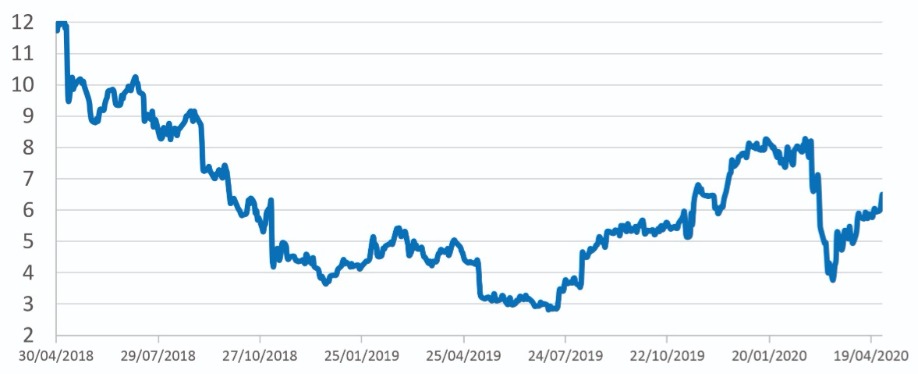
Infinera’s share price has shot up over the last twelve months, but is still below its value from April 2018.
From bottom to top
It’s been an encouraging 12 months for Infinera, the vertically integrated manufacturer of telecommunication equipment. This US-based firm has moved from last place on our Leaderboard to pole position, thanks to a share price that climbed from below $5 in late April 2019 to almost $8 by the end of the year and did not suffer from a substantial decline during the first few months of 2020. Note, however, that Infinera’s current valuation is still well short of the April 2018 price of almost $12.
The reasons behind both the rise in Infinera’s share price and the fall in its valuation over the last few years are illustrated in the company’s financial results. Take a look at the figures for the fourth fiscal quarter 2019, reported on 25 February 2020, and you’ll see that the profitability realised several years ago is either tiny or gone, depending on how you do the accounting, but gross margins and sales are heading in the right direction. Revenue for the fourth quarter exceeded guidance, hitting $384.6 million, which is up $59.3 million sequentially and a gain of $52.5 million compared with the equivalent quarter of 2018. Meanwhile, gross margin for the fourth quarter is 29 percent, up 2.3 percent sequentially and an increase of 3.6 percent year-on-year – but well short of the values north of 40 percent, reported around 2015.
During a call discussing fourth fiscal quarter earnings on 25 February, those leading the company painted a promising picture for the future. Reasons for an upbeat outlook included growing revenues, a diversified customer base and an expanded product portfolio.
According to company CEO Tom Fallen, fiscal 2020 will witness an important milestone in Infinera’s high-performance optics – it will mark a transition to fifth-generation, 800-gig capable technology that features digital signal processing (DSP).
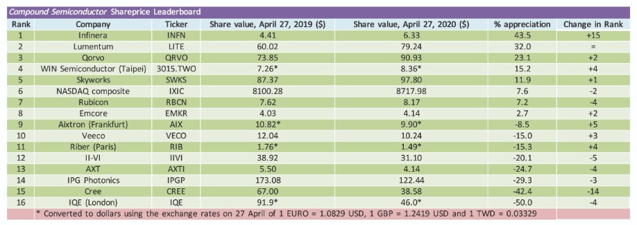
Share price leaderboard 2020
In his opinion, vertical integration, which has historically provided a way to reduce cost, is now critical to success in the market place. And this is good news for Infinera, as it limits the number of competitors.
“We do not see commercial optical components being broadly available for 800-gig until late this year or 2021,” claimed Fallon. “By designing and manufacturing our own DSP and optical components, we expect to deliver 95 gigabaud fifth-generation optical systems to the market before commercial components are widely available.”
Another development that Fallon expects to aid Infinera is the prioritisation of 400-gig products by commercial DSP manufacturers. “This creates a scarcity in sources of supply for 800-gig technology and opens a tremendous opportunity for those that are vertically integrated and early to market.”
Infinera remains on track to deliver 800-gig product during the second half of this year, with revenues expected to ramp in 2021.
During the February earnings call, Infinera provided a financial outlook for the future. For the first fiscal quarter 2020 revenue is expected to be $315 million to $335 million. This figure included a $15 million impact from the coronavirus, due to ancillary merchant optics sourced from the Wuhan area.
Nancy Erba, Infinera’s CFO, also spoke in the call, providing an outlook beyond the third fiscal quarter. Back in February she said that the market that Infinera serves is expected to grow at around 6 percent – but it could be less than this, depending on the extent of the Covid-19 outbreak. She predicted that Infinera’s growth would outpace this, due to the positioning of its portfolio, with gross margin climbing by 2 to 4 percent in both fiscal 2020 and fiscal 2021. “Into 2022, we expect to continue growing faster than the market and achieve our target business model of gross margins in the mid-40 percent and double-digit operating profit,” said Erba.
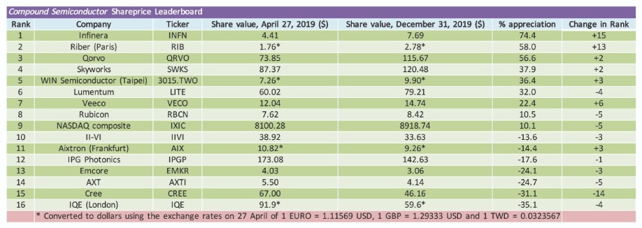
Share price leaderboard for the time period up until the end of December 2019
The most recent quarter has not been a good one for the company. While revenue met guidance, with sales totalling $331 million, gross margins dived to 23.3 percent, 5 percent below expectations. This did not go down well with investors, as the share price plummeting by more than 10 percent.
One of the reasons behind the fall in gross margin is the involvement in a subsea consortium build, coming a quarter early. The other issue is related to substantial shipments of the company’s 200-gig Groove solution, which is based on merchant optical engines.
Fallon revealed during the call that during the quarter Infinera experienced supply chain disruptions, due to many countries imposing public health restrictions that impacted the production and delivery capabilities of the company’s vendors around the world. “This disruption had a negative impact on our ability to fulfil certain customer requests during the quarter.”
Looking ahead, Fallon is concerned that the macroeconomic uncertainty felt by Infinera’s customers could more than offset the continued expansion of bandwidth demand. “To address this uncertainty, we are taking proactive measures to reduce operating expenses and improve gross margin.” Measures that taken include a temporary reduction of salaries for senior management and the Board of Directors, and staffing reductions, largely in the area of contract positions – they are said to have little impact on the company’s regular global worker force.
These steps are expected to deliver savings of between $5 million and $7 million, and should have an impact on results for the second fiscal quarter. Guidance for that is revenue of between $310 million and $330 million, and a gross margin of 27 percent to 31 percent.

Qorvo claims that it is supporting Samsung’s Galaxy S20 platform with a broad set of high-performance, highly integrated components.
Up one place from last year, Lumentum is now taking second spot on our Leaderboard, thanks to a share price that has risen from around $60 to $80 during the last twelve months.
The increase in the valuation of this manufacturer of many forms of laser reflects an improved balance sheet. For example, for the second fiscal quarter of 2020, ending on 28 December 2019, sales netted a record $457.8 million, up $7.9 million sequentially and $84.1 million year-over-year. Gross margins also improved over that timeframe, increasing from 33.4 percent for the second fiscal quarter of 2019 to 37.3 percent and 41.3 percent for first and second fiscal quarters of 2020, respectively.
On 5 May the company reported the results for the third fiscal quarter 2020. For that three-month period, ending on 28 March 2020, the Covid-19 pandemic had a significant impact on sales and margins. Quarterly sales dropped to $402.8 million – that’s $10 million below prior guidance given on 4 February that anticipated an impact from the pandemic of $15 million to $20 million. However, this shortfall did not alarm investors, nor the lower guidance for the fourth quarter, with the share price nudging up a few percent following the release.
During the call on 5 May, company CEO and founder Alan Lowe explained that the pandemic is expected to diminish fourth fiscal quarter revenue by more than $90 million: “Little more than half of this $90 million is a result of our inability to supply communication products, due to both component sourcing and production limitations – and the balance is from reduced consumer and industrial market demand.”
While the short-term impact of Covid-19 is not good for business, the changes it brings in the longer term could be, reasoned Lowe. “We believe Covid-19 will accelerate the shift to increasingly digital and virtual approaches to work, entertainment, education, health care, social interaction and commerce around the world.”

In autumn 2019 Lumentum moved its headquarters to a three-building office campus, known as Ridder Park Technology Center.
Lowe provided a great deal of detail on the impact of the pandemic on the company’s various facilities.
At Lumentum’s factory in Shenzhen, China, many employees worked through the Chinese New Year holiday so that the company could quickly ramp production at the factory when the nation returned to work. But this plan has been hampered by difficulties in obtaining components from third-party suppliers inside and outside China. The situation is improving, but will have some impact on fourth-quarter results.
Lowe explained that at the Thailand facility, employee protective measures were rapidly implemented in the third quarter. “These measures had not limited output so far, but production in Thailand has been impacted by the same challenges that our Shenzhen factory is experiencing with sourcing components.”
In Malaysia, Lumentum has a contract manufacturing partner for most of its telecom transmission products. Due to local government action to address the pandemic, production halted for several weeks from mid-March, and has been slowly ramping since then.
Operation continues at Lumentum’s wafer fabs, located in the US, Japan and the UK. They are used to make datacom chips, telecom transport and commercial laser products, and telecom transmission products, respectively. At these sites, social distancing measures are a drag on efficiency.
Like many companies, staff that can work from home are doing so. “The increase in network traffic we have created with our virtual meetings, where we have added more than one million median minutes per week since early February, is an indicator of bandwidth growth,” said Lowe, citing this as further evidence that the future is very bright for Lumentum.
Before the Covid-19 outbreak, demand for Lumentum’s telecoms and datacom product lines was “very strong and accelerating”, according to Lowe, with volumes constrained by supply. Demand maintained its strength throughout the third quarter, but revenue fell 6 percent, with the pandemic exacerbating existing supply challenges. Despite these issues, Lumentum continues to grow its sales for voltage-controlled oscillators and InP high-bandwidth products for 600 gig and 800 gig systems.
Lowe revealed that quarter-on-quarter sales for the telecom transport product line were “approximately flat”, while datacom chip revenue climbed 20 percent sequentially.
Due to seasonal factors, Lumentum’s revenue from its industrial and consumer product lines fell by 24 percent compared with the previous quarter. However, sales were up 40 percent year-over-year.
In the third quarter, the company ramped production of its lasers for world-facing cameras and LiDAR for consumer applications. But now, due to Covid-19, sales of its lasers for 3D sensing are expected to drop by more than 40 percent, due to weak consumer demand and the potential for smartphone supply challenges.
A decline in fibre laser sales during the third quarter led to a $43.5 million fall in revenue. “We expect over the next several quarters, that our fibre lasers business will soften further, as it is tied to growth in global manufacturing,” said Lowe.
Despite the uncertain future, Lumentum is recruiting. At its facility in the UK, it hopes to add around 200 staff so that it can ramp its transmission products.
The company is giving to its community during the outbreak. “We have used our commercial supply chains to procure and donate personal protective equipment to health care providers,” said Lowe. In addition, Lumentum has expanded its charitable donation programmes, and its staff have been using internal capabilities to produce and donate limited quantities of PPE.
Qorvo: 5G growth
Another company that has seen a gain in valuation after releasing its latest quarterly results is Qorvo. It has taken third spot on this year’s Leaderboard, just outperforming peers WIN Semiconductor and Skyworks.
Qorvo’s balance sheet shows that it is going from strength to strength. For fourth fiscal quarter 2019, ending on 28 March 2020, sales netted $787.8 million, up $106.9 million year-over-year, while gross margins climbed by 3.4 percentage points to 42.6 percent.
Uptake of 5G is helping to swell sales. “Products like our 5G ultra-high-band solutions are being adopted across customers and on all leading 5G chipsets,” said company President and CEO Robert Bruggeworth during fourth quarter earnings call on 7 May. Some of these products, including what is described as mid-high-band and ultra-high-band 5G solutions, are going into Samsung’s Galaxy S20 platform.
Further sales related to 5G are coming from shipments of GaN high-power amplifiers and small-signal components supporting sub-6 gigahertz 5G networks. “Demand for Qorvo’s products has been robust, driven by the ramp of massive MIMO antennas,” says Bruggeworth.
The capabilities of Qorvo have grown this year through the acquisitions of Custom MMIC and Decawave. The former strengthens the portfolio of GaAs and GaN RF products for defense and aerospace, while the latter provides ultra-wide-band technologies for proximity awareness, secure payments, and secure access for smartphones, automotive and IoT.
Qorvo’s factories and engineering labs are remaining open during the pandemic. In addition, product development schedules are running, design and engineering teams are still developing new technologies, and the company is continuing to have strong interaction with its customers.
However, revenue will be down in the next quarter, due to the consequences of the Covid-19 outbreak. This is not impacting all product lines: while sales of mobile products are expected to fall, those from the infrastructure and defence division are expected to rise, thanks to greater demand for 5G infrastructure and the latest generation of Wi-Fi technology.
Based on all these considerations, revenue for the first fiscal quarter of 2020 should be between $710 million and $750 million. This range is wider than normal, reflecting greater uncertainty in the markets and the broader economy due to the effects of Covid-19.
IQE’s decline in income
Footing this year’s table is international epiwafer supplier IQE, which has seen its share price halve during the last 12 months. This fall reflects a decline in annual revenue from £156.3 million in 2018 to £140 million in 2019, resulting from reduced sales to a wireless customer that has been affected by changes in global markets and a photonics customer that has suffered from technical issues that are not related to IQE’s wafers.
Another key insight provided by the full year results, released on 28 April, is that despite the loss of a photonic customer, IQE’s revenue from this division increased by 4.4 percent to contribute £66.8 million, with half of those sales associated with VCSEL products. Meanwhile, wireless revenue fell by 22.4 percent to £68.2 million, due to a significant decline in volume from a GaAs power-amplifier customer. Loss in revenue has impacted the bottom line.
According to adjusted operating figures, IQE made a loss of $4.7 million last year, compared with a profit of £16 million in 2018. Company finances have not been helped by a bill for £4.3 million for legal costs, associated with a confidential patent dispute.
The Covid-19 pandemic is not having a major impact on production capability, with all sites around the globe remaining operational. As is the norm in the industry, staff are working from home where able. Other changes to operations include an increase in cleaning regimes and planning for shift segregation.
The outbreak has created much uncertainty in the market, and has led IQE to withdraw from offering specific guidance. However, it did reveal that its first-quarter trading exceeded expectations, and described the outlook for the second quarter as “positive”.
In the last few years, IQE has invested in infrastructure that should lead to higher margins and increased capacity. It has built a large foundry in Newport, South Wales, that has started to manufacture 3D sensing products; it has increased it wireless capacity in Taiwan to address changes in global supply chain dynamics; and it has built GaN capacity in Massachusetts to capitalise on forthcoming 5G infrastructure deployments. With all this in place, investment in property, plant and equipment is expected to significantly reduce in 2020 to below £10 million.
Despite the uncertainty in the near-term, IQE continues to invest in the generation of new products. It will spend £10 million this year developing: 10G and 25G distributed feedback lasers and avalanche photodiodes for high-speed datacoms and 5G fronthaul and backhaul; 5G switches and filters, which are based on its patented crystalline rare-earth oxide technology; long-wavelength VCSELs for future smartphone and LIDAR deployments; and lasers and sensors for environmental and health monitoring.
Such investment should serve IQE well. While the near-term may be tough, it has much promise for the future. It share price will surely rise, and like many companies from different sectors in our industry that have found themselves footing the table, it has the potential to rapidly climb up our Leaderboard.
Custom-based modules made from SiC MOSFETs minimise the impact of short circuits and overloads
BY DENIS KOUROUSSIS FROM ATOM POWER
At some point in the career of nearly every electrical engineer they would have wondered whether it is possible to design a circuit breaker that is not mechanical in nature. Many will reason: Isn’t it better to use a semiconductor to break a fault or handle an overload?
However, when they delve more deeply into this issue, they’ll start to run into roadblocks. One is that the power devices that they are familiar with have a breakdown voltage of around 600 V, so many of them would have to be stacked in series, even when making a circuit breaker for a low-voltage industrial applications that runs off a 480 Vrms AC supply.
Another issue is that when the power flows through any semiconductor device, it creates substantial heat, due to resistances that are significantly higher than those of traditional metal contacts. As this heat must be dissipated, the entire architecture of today’s circuit breaker has to be ‘re-thinked’, before starting to design this product.
Given all these challenges, why would you want to make a solid-state circuit breaker? After all, aren’t the existing mechanical ones, which have been around for over a century, up to the task?

Figure 1
Combatting arc flash
Unfortunately, mechanical breakers are far from ideal in the electrical circuit protection space where by far the biggest problem is arc flash. That’s the name for the amount of energy let through during a short-circuit condition. When mechanical circuit breakers attempt to shut off the current, there is a delay associated with opening this device of typically 8 ms or more. Although a mechanical response of 8 ms is extremely fast for a mechanical contraption – it is probably the physical limit for a metal contact disconnection – in electrical terms it is a ‘lifetime’. During those precious milliseconds a short-circuit fault current can develop from a power source that provides as much as 10 kA or 100 kA, depending on the size rating of the upstream transformer. In this situation, energy dissipates at the fault, with a value that is proportional to the square of the current, which varies with time. At this fault, the flow of energy is often so rapid that it creates an arc blast of molten metal. It is only after this, when the fault current reaches levels of 10 kA or 100 kA, that the circuit breaker will dissipate a significant arc internally upon opening, in order to extinguish the particular massive fault current.
Some good news is that there are benefits associated with the power that comes from the national grid, due to it being in AC form, rather than DC. This means that at least the fault current crosses zero at some point during the half cycle, helping to extinguish the arc within the circuit breaker.
During the past two decades, there have been more initiatives focusing on educating engineers about arc flash. However, efforts have not tackled the origin of the problem head-on, because it is not possible to increase the mechanical speed of opening contacts. Instead, programmes have aimed at minimising the damage that arc flash can cause. This has led to reinforcing both switchgear and the casings of protective devices, as well as training technicians, so that they understand what the appropriate personal protection equipment is for operating circuit breakers and for working near live equipment. In addition, the electrical industry has started to adopt current-limiting breakers and current-limiting fuses that trim the short-circuit current.
But none of these approaches are ideal. The real solution is to open faults within microseconds or less, so arc flash is never a problem. As solid-state circuit breakers make that possible for the first time, they promise to revolutionise electrical infrastructure.
The challenge of selective co-ordination
When engineers try to ensure electrical protection, they need to consider the issue of selective co-ordination. In every electrical distribution system, any fault in the system must be cleared by the closest circuit breaker upstream. This must be accomplished without bringing down the entire electrical distribution system. As mechanical circuit breakers have large varying tolerances for their time curve characteristics, the upstream circuit breaker must have a longer time delay for its time curve characteristics than any downstream breaker.
To illustrate this point, and consider its ramifications, imagine an industrial application with a 2000 A circuit breaker straight from the utility mains. This is feeding a downstream breaker of 150 A that supplies a chiller system. The
150 A breaker for the chiller may have an opening time between 8 ms at best and 13 ms at worst. By knowing this spread, defined in the time curve characteristics provided by the manufacturer, an engineer can apply best practice. To ensure that the entire facility does not drop power if there is a short circuit in the chiller, the engineer requires the upstream 2000 A breaker to have a best opening time of longer than 13 ms. Due to the wide time band that the 2000 A breaker will have, it needs to have an average opening time of 20 ms or more, compounding the challenge of arc flash.
In stark contrast, solid-state circuit breakers are not impaired by the mechanical limitations in clearing time. Thanks to this, they offer a faster response at the point of fault, reducing the time required for a co-ordinated response from the overall circuit protection system.
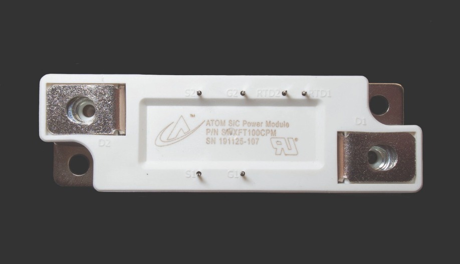
Figure 2
The SiC solution
Efforts to develop solid-state circuit breakers have been aided by developments in other industries. During the last ten years, electric vehicles have started gaining traction, creating demand for more efficient converters operating at higher voltages. Success is highly prized, as it increases vehicle efficiencies and enables that most coveted of assets – a longer driving range. Key to realising this are more efficient devices with lower on-resistances and minimal losses. If these devices are operated at higher voltages there is less current for the same power, enabling a reduction in the use of copper and other conducting materials, and ultimately reductions in weight and cost.
Several companies have invested heavily in developing SiC devices. Efforts have led to MOSFETs, IGBTs and JFETs that can block up to 1700 V, while offering a far lower on-resistance than their traditional silicon counterparts. SiC power devices also switch far faster, enabling inverters to be smaller, have lower switching losses, and potentially retail for less. Thanks to all these advances, SiC devices are the prime candidates for low-voltage circuit protection.
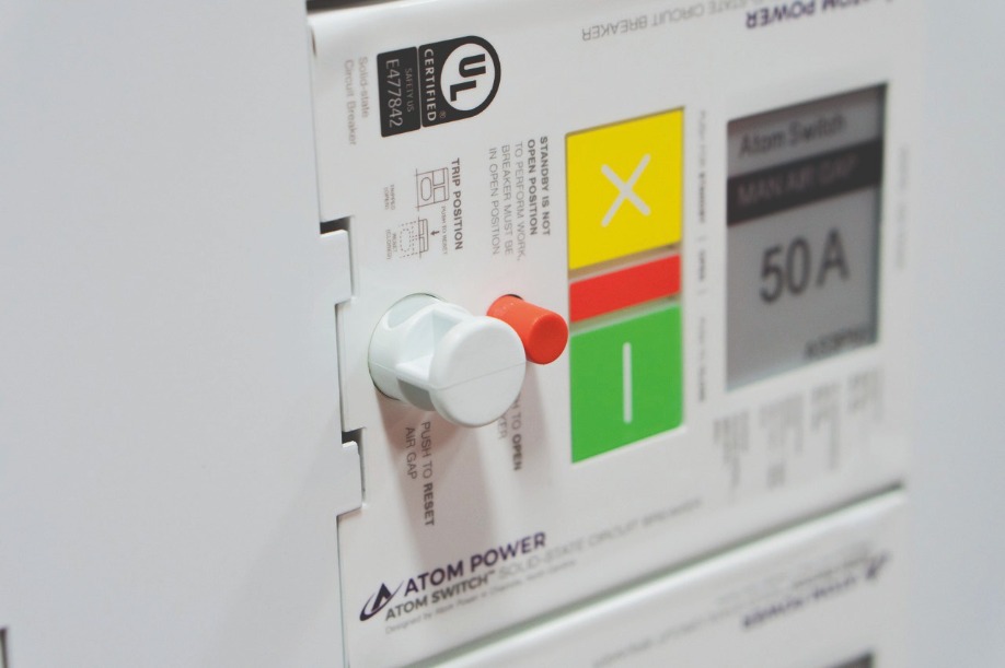
Figure 3
Note that the majority of applications for these off-the-shelf devices are in the inverter markets, providing DC to DC, AC to DC, and DC to AC conversion. For these tasks, components are housed in discreet packaging, making them unsuitable for use in solid-state circuit protection. If off-the-shelf components were used to produce solid-state circuit breakers, the likelihood is that they would be too bulky. An additional complication is that when MOSFETs are deployed, they need to be in a common-source tied configuration to ensure that AC voltages can be blocked bi-directionally. Due to all these issues, solid-state circuit breakers require a custom module.
When designing a solid-state circuit breaker, it is critical to consider the on-resistance of the transistors. For a SiC MOSFET, this is in the range of 10-20 mΩ. That’s significantly better than comparable silicon devices, which may have an on-resistance 60 mΩ or more – and also a lower blocking voltage. However, even though the SiC MOSFET provides far better performance than its silicon counterparts, its on-resistance is still not trivial, due to the potentially large currents that it needs to pass. For example, if a SiC MOSFET with a 10 mΩ on-resistance has to pass 100 A, then the power it dissipates – the product of resistance and the square of the current – is 100 W. As that’s for just one device, and a circuit breaker will require two in series, dissipation will total 200 W. Such a high power will require a heat sink, and will reduce the efficiency of power delivery through the circuit breaker.
One of the virtues of using SiC MOSFETs is that when they are arranged in parallel, they share current very well, thanks to resistances that are proportional to temperature. Consider two of these transistors in parallel: as current passes through one of them, it heats up the die and resistance rises, effectively pushing current through the second die until the temperatures and resistances balance.
When SiC MOSFETs are placed near to one another on the same substrate, their temperatures are closely linked. Using this approach, one can produce a symmetrical layout that ensures not only current sharing, but equivalent values for stray inductances, capacitances and inherent resistances of metal conductors. With such an architecture, designers can ‘parallelize’ as many devices as they wish, theoretically lowering the on-resistance to any level. In this case, the limiting factors for the size of the SiC area used to trim the on-resistance are the financial implications, and the form factor for the solid-state circuit breaker.
Module design
When an engineer designs a module for solid-state circuit protection, their considerations are markedly different from designing one for an inverter. The latter incorporates high-speed switching, and will have minimal inductances and capacitances to ensure low losses. In contrast, with a circuit protection device, there is no need to consider switching in any form. That’s because this device will be conducting for the majority of its life, and there will only be a handful of turn on or off events.
What is important when designing a circuit protection module is to keep inductances and capacitances equivalent amongst parallel devices. This is critical when an overload or short circuit occurs, as currents can be significantly elevated within the module, and a balanced current needs to pass through all the parallel devices as the gate voltage is reduced (assuming an n-type device) to bring that elevated current to zero. Another requirement is that all the gate connections to the parallel devices have equivalent impedances, to ensure a uniform current turn-off profile amongst the devices. By fulfilling all of these principles, all devices will undergo the same level of electrical stress during a turn-off event, maximising the endurance and the reliability of the module.
Steps should also be taken to minimise the overall on-resistance of the packaged module. This includes considering metallization traces on the substrate and wire bonds, and maximising the cooling for each of the SiC power die, as this reduces the internal module and die temperatures.
At Atom Power, a start-up founded in 2014 and located in Charlotte, NC, we have followed all of these guidelines when designing our 900 V, 250 A power module (see Figure 2). It has a total on-resistance of 7 mΩ, and turn-on and turn-off times of 0.1 μs. Our module forms the basis of a solid-state circuit breaker that we have dubbed the Atom Switch (see Figure 3). It is the first of its kind to gain approval from the Underwriters Laboratory, an independent institution with responsibility for safety standards. Our Atom Switch is a UL489 listed product that virtually eliminates the risk of arc flash and effectively reduces tripping time, thanks to the correct packaging, including current sense, intelligence and control in the circuit breaker. We have tested our product under 100 kA, 150 kA and even 200 kA short-circuit conditions. In all cases it satisfies every requirement without any hardware modifications.
We have designed our Atom Switch to work within the Atom Panel. This provides proper mounting, as well as communications and sufficient thermal transfer to ensure that modules keep cool (see Figure 4).
With our Atom Switch, there is a typical delay of 40 μs for opening under a short-circuit condition. That is far longer than the time taken for the module to switch – that is around 0.1 μs – with the difference coming from a combination of the delay of fault-current rise time of the short circuit, and detection and signalling to turn off the module on the event. However, 40 μs is still incredibly rapid, given that it’s 200 times shorter than the fastest mechanical circuit breakers on the market today. By opening so fast, the energy that is let through falls by a factor of 4000.
An additional benefit of our SiC-based circuit breaker is that unlike a mechanical breaker, it does not need replacing after it has interrupted full-rated short-circuit currents a few times. Yet another merit is that for low overload conditions that are one-to-two times the current rating, the tripping characteristics can be set extremely precisely, with a less than a 1 percent accuracy for tripping time. In comparison, for mechanical circuit breakers, the allowance is up to 10 percent.
Our next generation of Atom Switch will incorporate a ground-fault circuit interrupting capability and an arc-fault circuit interrupting capability. These innovations, realised by employing significantly more algorithmic implementations, will address a significant proportion of nuisance tripping, which is an issue in mechanical circuit breakers – in particular, they struggle to cope with arc-fault circuit interrupting.

Figure 4
Making an even more compelling case for our solid-state circuit breakers are the numerous additional advantages of this technology. One of its benefits is the opportunity to adjust the time curve characteristics through software, so a product can be used for multiple applications, or re-used when the equipment is placed in a different environment.
Additional attributes include self-maintenance and diagnostics. As the solid-state circuit breaker can incorporate intelligence, it can: effectively self-diagnose its own functionality, and ensure correct operation; and generate an alert when a problem has developed, thereby preventing a catastrophe. With mechanical breakers, that’s not possible, as problems are only detected after a fault has occurred, which often ends in a catastrophic event that causes significant damage. Another feature of the solid-state circuit breaker is its remote controllability, making it a great candidate for both demand-management applications and for microgrid islanding, where back-up and alternative power sources may be used. And yet another feature of the solid-state circuit breaker is providing a soft-starter for induction motors and transformers, by emulating a silicon-controlled rectifier.
Today, our solid-state circuit breakers command a higher price tag than their ‘equivalent’ mechanical counterparts. But they are vastly superior on many fronts, offering safety and features that far surpass the capabilities of traditional circuit protection equipment. Due to these merits, their use can eliminate additional equipment deployments, or meet critical safety concerns, making them an attractive purchase.
There is good reason to believe that the cost of these solid-state units will fall, due to a ramp in SiC device production to cater for electric vehicle production, smart-grids and solid-state circuit protection. While mechanical breakers will not disappear overnight, it’s clear that their days are numbered.
Dedicated, carefully constructed models allow VCSEL designers to evaluate the consequences of temperature on the gain, output power and spatial profile of the device
BY DOMINIC GALLAGHER FROM PHOTON DESIGN AND Sam Shutts FROM THE University of Cardiff
One of the biggest selling devices within today’s compound semiconductor portfolio is the vertical cavity, surface-emitting laser (VCSEL). Its meteoric rise is evident in a recent announcement by Trumpf, boasting that it has shipped two billion of them. Many of these devices will have been deployed in mobile phones, such as those made by Apple, which uses hundreds in its Face-ID function.
Manufacturing VCSELs involves a series of steps that differ from those used for the production of conventional, edge-emitter lasers. Making the latter involves dicing a processed semiconductor wafer into small chips. Light is emitted out of their edge, creating a horizontal lasing cavity.
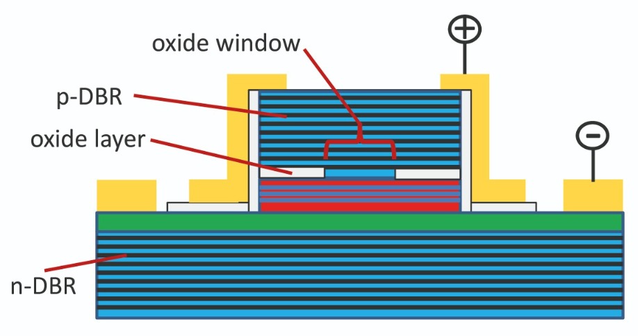
Figure 1. A typical VCSEL structure contains an active layer sandwiched between a pair of mirrors: an n-DBR (distributed Bragg reflector) and p-DBR. Current makes its way through the mirrors to the active layer.
For designers, the VCSEL presents a number of challenges. Like all forms of laser, it features a gain medium surrounded by a pair of mirrors. As light bounces between them, criss-crossing the gain medium, optical losses occur on each round trip. These losses must be compensated by optical gain. That’s a relatively easy requirement to fulfil in a typical edge-emitting laser diode with a 200 μm waveguide that amplifies the lasing light – a mirror with a 50 percent reflectivity is sufficient to double optical intensity in a single pass. In comparison, a VCSEL must achieve the same with a gain region of just 0.1 μm. This demands mirrors that reflect well over 99 percent of the light. While fulfilling this criterion, the light absorbed or scattered inside the cavity must be minimised. If just 0.5 percent of the light is lost in this manner, that still enough to severely impair device efficiency.
To produce mirrors with such a high reflectivity, engineers grow a stack of alternating high and low refractive index layers (see Figure 1). To help them with this task, they want to turn to modelling – but great care is needed to ensure that the results are valid. Modelling VCSELs is far from easy, as the level of accuracy that is acceptable in most devices – normally a few percent is fine – simply will not do. If conventional modelling were to use a mirror reflection loss of around 1 percent, and a similar value for the transmission loss, it would deliver a nonsensical result.
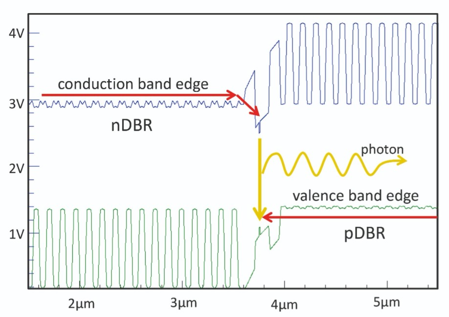
Figure 2. Band edge diagram through the axis of a VCSEL.
Clearly, what’s needed to support the designers of VCSELs is a dedicated, reliable, multi-disciplinary simulation tool. Serving this need is Harold/VCSEL, a tool developed by Photon Design, a company based in the UK that one of us works for. This simulation software, which is capable of modelling most of the subtleties of the optical and electronic properties that are at play in a modern VCSEL, has been used by our other co-author, an academic at Cardiff University, during the production of devices that can serve in a real-life application – atomic clocks.
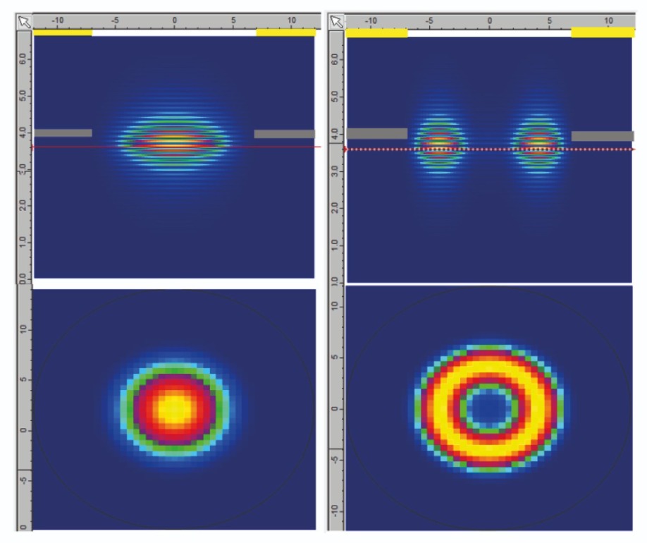
Figure 3. The cavity modes of a VCSEL – top row: side view and bottom row: plan view.
To sustain lasing in a VCSEL, the mirrors of this device must have reflectivities of at least 99.5 percent. Helping to accomplish this are the Distributed Bragg Reflectors (DBRs) – stacks of layers with different refractive indices that produce periodic reflectivity. But these reflectors, on their own, are insufficient – the VCSEL must also confine the light laterally. In particular, there is a need to keep the cavity mode away from the walls of the VCSEL, where losses increase.
The common way to accomplish this is to include an ‘oxide aperture’. This is created by oxidising one or two epitaxial layers inwards from the walls of the device to form a light-guiding ring with a lower refractive index (see Figure 3 for an illustration of cavity modes). Using this design, current is injected into the laser via a ring contact on the top surface.
Carriers flow through the DBR to get to the active region (see Figure 1). Unfortunately, this modus operandi is exactly what you don’t want, with the current highest at the tip of the oxide window, and lowest at the peak of the fundamental mode, which occurs in the middle of the VCSEL axis (see Figure 4). When this happens, higher order modes are favoured.
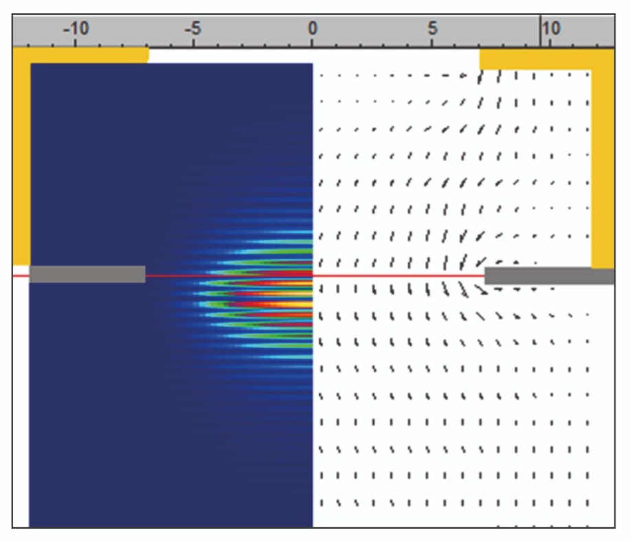
Figure 4. Cross-section of a top-contacted VCSEL, showing the computed mode on the left half and the current flow on the right half.

Figure 5. A side-injection VCSEL, with current bypassing the top DBR stack.
The output power of the VCSEL is primarily limited by the heat generated within this chip. It comes from a combination of electrical resistance, non-radiative charge recombination, absorption of photons and, particularly, a process known as Auger recombination (see Figure 6).
One of the contributors to the electrical resistance is the interfaces in the DBR mirrors. Add more layers, and this resistance increases.
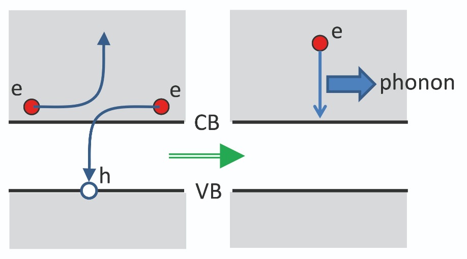
Figure 6. One of the significant loss mechanisms in the VCSEL is Auger recombination. When two electrons in the conduction band collide, this can cause one to recombine with a hole, while the second is excited further up the conduction band. The result is that the excited electron is converted to heat. This problem gets worse at longer wavelengths.
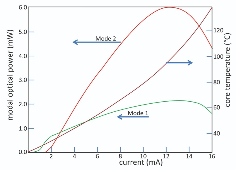
Figure 7. Light-current curves of a VCSEL, showing saturation at high currents.
Obviously, one of the goals for a VCSEL designer is to minimise heating within the device. To succeed, it is crucial to compute the heating profile and the resulting temperature distribution. Modelling with the Harold/VCSEL tool offers much insight, as shown in the plot of the temperature profile of a device driven at 16 mA (see Figure 8), using a 20 °C background temperature. In this VCSEL, there are two cavity modes. The fundamental mode starts lasing at 1 mA, but very soon a second, donut-shaped mode starts lasing. It first appears at 1.5 mA, and quickly dominates.
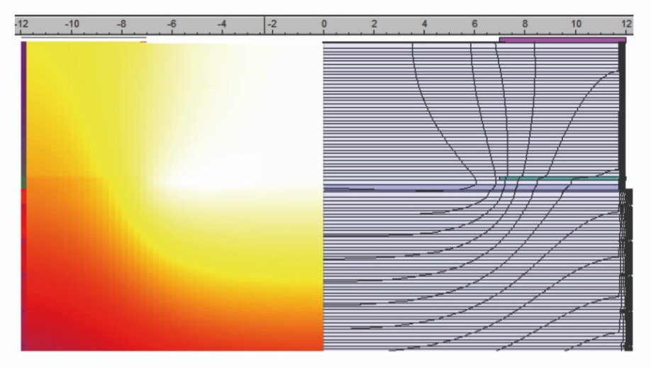
Figure 8. Temperature profile in a VCSEL, drawn as a heat-map (left) and contour plot (right).
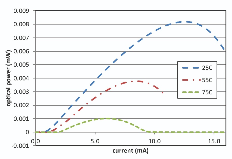
Figure 9. As the background temperature increases, VCSEL performance can drop dramatically. The graph shows the light-current curves for the same VCSEL at 25 ˚C, 55 ˚C and 75 ˚C.
The downside of increasing the diameter of the oxide window is that it leads to multi-mode VCSEL operation. This is acceptable in many applications, so most commercial VCSELs are multi-mode. However, such devices are not really suitable for driving single-mode fibre data links – the workhorse of the datacom industry.
What may come as a surprise is that there is actually a major benefit to be had from these additional modes. Simulations show that if all the modes are artificially suppressed, save the fundamental optical mode, peak power plummets (see Figure 10). Spatial hole burning is to blame, with the low-intensity single-mode concentrated in the middle of the oxide window where the current is highest. Here the electron density builds up at the rim of the window, creating increased Auger recombination and heating. It is better to have more modes, as this ensures a more uniform optical intensity and thus a more uniform electron density.
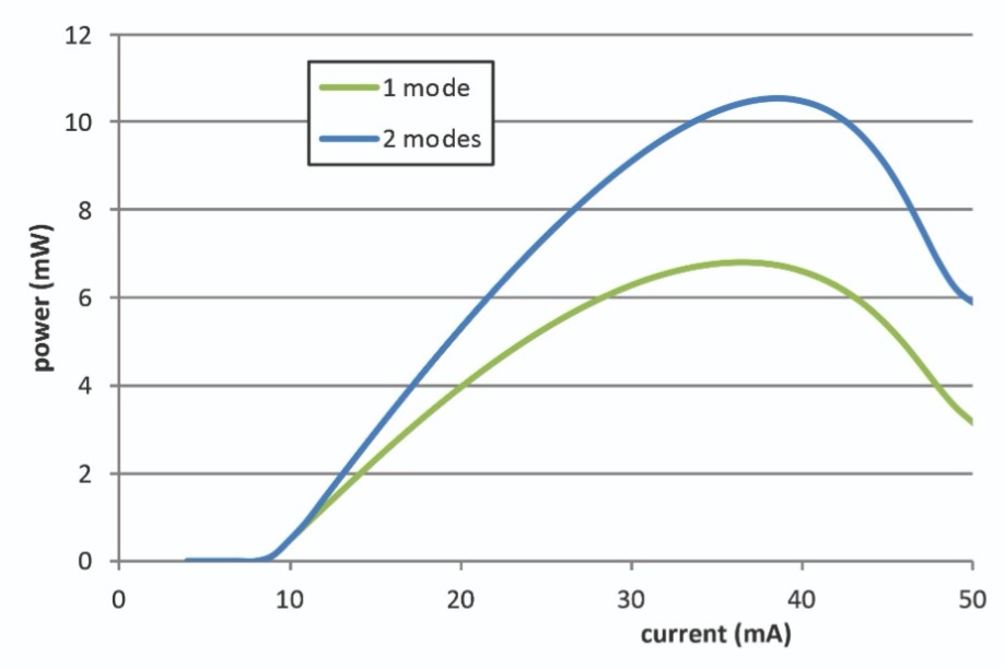
Figure 10. Light-current curves for a VCSEL, supporting two modes (blue). The second mode is suppressed (green).
The trick to improving linearity is judicious detuning of the mode resonance away from the gain peak. This is illustrated in Figure 11. Instead of aiming to operate the VCSEL at its room-temperature gain peak, de-tuning may be applied, leading to a far smaller reduction in gain at elevated temperatures.
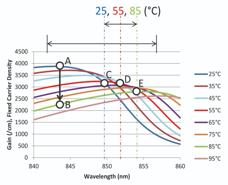
Figure 11. Computed gain spectra of a GaAs VCSEL at different temperatures. As the VCSEL heats up the gain peak moves to a longer wavelength and decreases. If the VCSEL had been designed to operate at the 25 ˚C gain peak (A), then when at 85 ˚C the gain would fall to point B. It is better to detune the VCSEL to operate at point C at room temperature, as then the gain drops by only a small amount at 85 ˚C – point E.

Figure 12. (left) A VCSEL that contains a suspended-grating for the top mirror. (right) the electric field generated by a plane wave incident on the grating from below – note the near absence of light above the grating.
Applications for VCSELs are not limited to facial recognition and datacoms. These sources can also serve in several specialist applications, including low-power atomic sensors for precision timing. Within today’s digital infrastructure, precise clocks are critical for synchronisation. These clocks rely on signals from a global navigation satellite system for a precise timing reference. However, the satellite systems are vulnerable to incredibly costly outages, caused either accidentally or by malicious attack. If, for example, a widespread outage were to occur in the UK, it could cost the nation’s economy £1 billion per day. One solution, under development at Cardiff University and its partners, is a ‘chip-scale’ atomic clock. It could be placed within the required locations to provide a backup in the event of an outage of the global navigation satellite system.
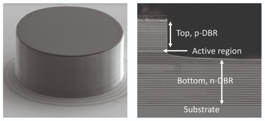
Figure 13. Side view (left) and cross-section (right) of an etched VCSEL mesa, manufactured by Cardiff University’s Institute for Compound Semiconductors.
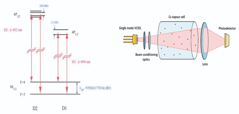
Figure 14. (left) The Caesium electron transitions used for an atomic clock targeting 894.6 nm (D1 line). (right) A caesium clock vapour cell excited by a VCSEL (courtesy of UK National Physics Laboratory).
To meet these specifications, a team led by researchers at Cardiff University has turned to modelling using the Harold/VCSEL tool. As well as aiding the design of the VCSEL epi-structures and device geometries, modelling assists interpretation of device results. What’s more, it offers tremendous insight into whether characteristics should be attributed to the fabrication method, or are caused by epi-growth or design.
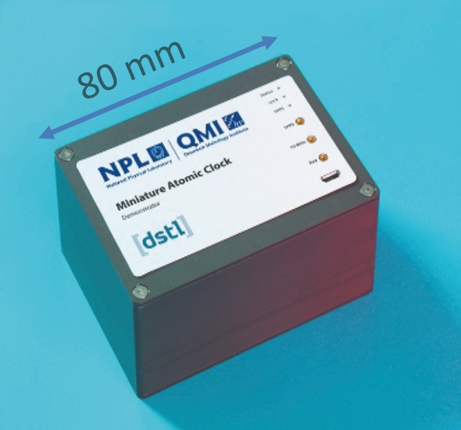
Figure 15. A packaged Caesium atomic clock with VCSEL pump (courtesy of University of Cardiff, UK National Physics Laboratory and DSTL).
On top of all these considerations, met through careful selection of the composition and thickness of the layers in the epi-design, there are other factors that affect VCSEL performance. They depend on the way the device is fabricated.
One factor that has great influence over the performance of the VCSEL is the oxide aperture.
As atomic clocks require VCSELs to have single-mode emission, the oxide aperture is restricted to a diameter of typically no more than 3 μm. Having such a small aperture has two significant effects: it results in locally high current densities, and it alters the effective index in that region of the cavity.
The performance of the VCSEL is impaired by the high current density, which increases further with injection current. This leads to joule-heating, which can have deleterious effects not only on the optical power output, but also on the emission wavelength. Changes in power are not a major issue, as 1mW of optical power is sufficient for an atomic clock – but the wavelength is a critical parameter that needs to be precisely defined. Unfortunately, heating can shift the emission wavelength outside the intended design specification, and complicating matters even further, there can be an additional shift in emission wavelength resulting from a change in effective index, which moves the cavity resonance.
The solution is to use modelling to account for the shifts in wavelength with injected carriers and effective index variation, so that these effects can be compensated for in the design of the epilayers. Such modelling is an invaluable tool for the development and manufacture of VCSELs, which are already being produced in their billions, with volumes tipped to rise in the coming years.
Gallium oxide MOSFETs run at lower temperatures and switch better when they are transferred to substrates with a higher thermal conductivity.
BY Wenhui Xu, YiBo Wang, Tiangui You, Genquan Han and Xin Ou from SIMIT CAS and Xidian University
In recent years there has been much interest in gallium oxide. The form known as β-Ga2O3 has great promise for high-power devices, thanks to its combination of excellent electrical properties, adjustable doping and the potential for low production costs.
However, before this class of device can take on the likes of SiC and GaN, two significant hurdles must be overcome. One is the low thermal conductivity, which is only one-tenth of that of SiC, and is to blame for the self-heating and ultimately the poor performance of power devices. And the other is the absence of p-type doping, which prevents the production of p-n junctions that hold the key to realising low turn-on voltages and ultra-high breakdown voltages.
It is well accepted that the issue of thermal management could be addressed by heterogeneously integrating Ga2O3 onto a high thermal conductivity substrate, such as silicon or SiC (see Figure 1). But what growth technologies can be used to realise high-quality Ga2O3 thin films on these foundations? Many researchers have tried and failed to grow thin films of Ga2O3 on silicon and SiC heteroepitaxially. Polycrystalline Ga2O3 results, due to the large lattice mismatch with the substrate.
An alternative approach is to use the (100) cleavage plane of Ga2O3 to transfer micrometre-sized pieces to silicon, SiC or diamond. This is successful, but the small size hampers the commercial application of this technology.
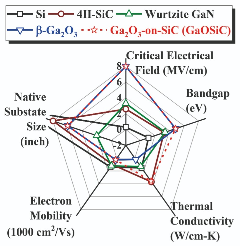
Figure 1. Ga2O3 has many material properties that are well-suited to power devices. k of Ga2O3-on-SiC (GaOSiC) is equal to that of SiC.
This approach has much promise for high-volume manufacture, given that ion-cutting and wafer bonding are used for the mass production of silicon-on-insulator wafers.
Drawing on our experience with these processing techniques, we have obtained an appropriate implantation fluence for H+ and He+ in Ga2O3 bulk. This is of vital importance for forming the micro-cracks, which are key to exfoliating Ga2O3 films.
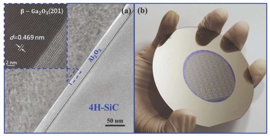
Figure 2. (a) Cross-sectional transmission electron microscopy of Ga2O3-Al2O3-SiC (GaOISiC). Inset shows the high-resolution transmission electron microscopy image of a single-crystalline β-Ga2O3 thin film on Al2O3. (b) MOSFETs on wafer-scale GaOISi.
Note that we employ an additional post-annealing process to improve the quality of the transferred Ga2O3 thin films. This step narrows the peak of the X-ray diffraction rocking curve – the full width at half-maximum shrinks from 280 arcsec to 140 arcsec. In addition, we use a chemical-mechanical polish to extricate an implantation-induced damage layer close to the top surface. This step reduces the surface roughness of the transferred Ga2O3 thin films to just 0.4 nm.
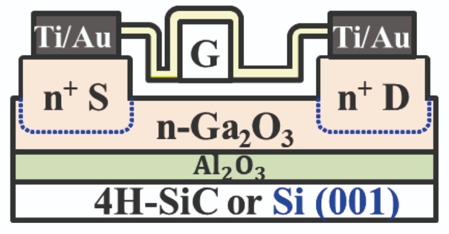
Figure 3. The architecture of the Ga2O3/Al2O3/SiC(Si) MOSFET.
On this template we have made a trench MOSFET, realising E-mode operation by varying the channel thickness (see Figure 3). When it is much less than 40 nm, the transistor is normally off, due to the interface states between Ga2O3 and the gate dielectric that depletes the carriers in the channel.
To lower the contact resistance, we turned to source and drain implantation. This reduced the specific on-resistance to 49 mΩ cm2. We have also added a field-plate structure, which has increased the breakdown voltage to 800 V (see Figure 4). An even higher value can be obtained by eliminating interface defects, plus those that are induced by ion implantation.
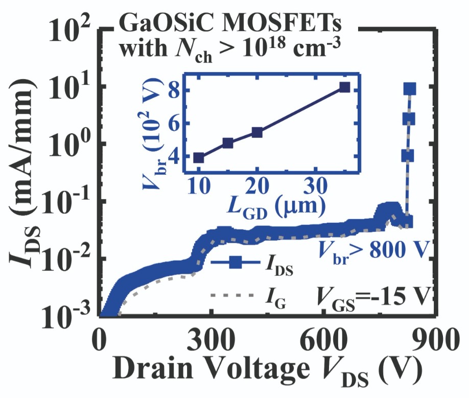
Figure 4. Three-terminal breakdown measurement of GaOSiC MOSFETs with a field plate. The inset show the breakdown voltage (Vbr) as a function of gate-to-drain spacing for separations up to 35 μm.
Our analysis of the thermal stability of our fabricated MOSFETs has included simulations. As expected, they show that the operating temperature of the device on a SiC substrate is smaller than that on the Ga2O3 bulk substrate. According to transient thermal reflection measurements, the thermal conductivity of Ga2O3-Al2O3-SiC is very close to that of SiC, and significantly higher than bulk Ga2O3.
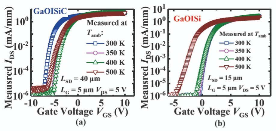
Figure 5. Transfer characteristics of GaOISiC and GaOISi MOSFETs measured at different temperatures.
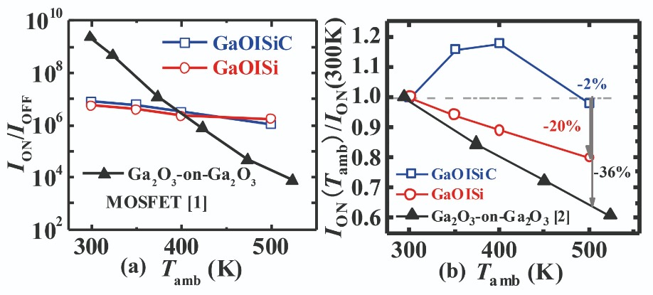
Figure 6. (a) On-off ratios show very little variation with temperature in GaOISiC and GaOISi MOSFETs, but do in Ga2O3-on-Ga2O3 devices. (b) As the ambient temperature (Tamb) increases to 500 K, GaOISiC and GaOISi MOSFETs show a 14 percent increase in on-resistance (Ron), a figure far lower than that of a Ga2O3-on-Ga2O3 device. Reference [1]: M. H. Wong et al. IEEE Electron Device Lett. 37 212 (2016). [2]: M. H. Wong et al. Appl. Phys. Lett. 109 193503 (2016).
It is well known that self-heating effects are generally not observed in the off-state, due to minimal power dissipation in the devices. The addition of an Al2O3 insulator between Ga2O3 and a silicon or SiC handle leads to a very stable off-state current. In comparison, in the devices with a foundation of bulk Ga2O3, as temperature rises there is a significant increase in the off-current, due to degradation of the insulating properties.
The production of a semi-insulating Ga2O3 substrate involves iron-compensation doping. This results in a high concentration of acceptor traps at the valence band. As temperature increases, traps release some of the electrons that are captured. The Ga2O3 remains weakly n-type, contributing to the increase in the off-current of the transistor. We have simulated the off-current distribution in different device designs, and our findings mirror the results obtained at room temperature and an elevated temperature (see Figure 7).
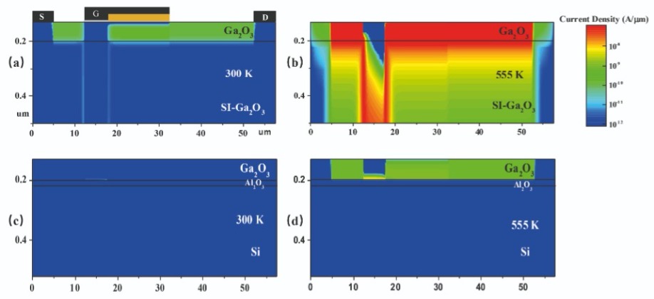
Figure 7. Simulations show a remarkable rise in the off-current at a drain-source voltage of 5 V in Ga2O3-on-Ga2O3 devices at 555 K compared with 300 K. (a) and (c) shows off-current distribution of Ga2O3-on-Ga2O3 and GaOISi at 300 K respectively; (b) and (d) show the off-current distribution of both structures at 555 K.
W. Xu et al. in IEDM Tech. Digest 2019 p. 12.5.1
Y. Xu et al. Ceram Int. 45 6552 (2019)
Doubling the supply voltage of an RF GaN HEMT increases its power per die area and enables a substantial reduction in the size of very-high-power systems
By Sebastian Krause from the Fraunhofer Institute for Applied Solid State Physics IAF
Recently, GaN HEMT technologies have been adopted in a variety of applications, ranging from power conversion to mobile communication. This broad uptake has been spurred by the superior intrinsic material properties of GaN compared with competing silicon-based technologies. Thanks to the many merits of GaN, engineers can construct more efficient, smaller systems that trim operating expenses.
The rollout of 5G has taken interest in GaN to a new high. Initially it had been viewed as the best candidate for serving the 3 GHz to 6 GHz range, but more recently it has been tipped to also succeed in a millimetre-wave domain that spans 24 GHz to 39 GHz. Its virtues include a higher power density than conventional silicon LDMOS and silicon CMOS processes, enabling a reduction in chip size, which is a critical factor in multiple-input, multiple-output (MIMO) systems. In addition, as each GaN single chip die generates more power than its rivals, losses in off-chip power combining networks are reduced, leading to smaller, more efficient systems.
For the same reasons, GaN is found in a growing number of applications demanding a very high output power. For several years it has been successfully deployed in civil and military radar, and it is now a proven solution for powering these systems.
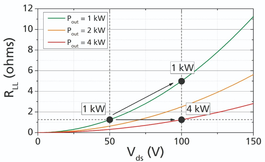
Figure 1. Load-line resistances of exemplary devices with output powers of 1 kW, 2 kW and 4 kW, plotted against supply voltage.
Due to the numerous applications for GaN devices, during the last decade many different variants of this technology have been brought to market. Some processes, specifically developed for power conversion, are supporting supply voltages up to 1200 V. However, for technologies targeting RF applications, such as radar and telecom, voltages have been restricted to 28 V to 65 V. The main reason for this discrepancy is the difficulty in combining a high breakdown voltage with a good high-frequency performance. Improve on one front, and the tendency is to compromise on the other.
Minimising network losses
For very-high-power applications – such as pulsed and CW radar, particle accelerators, plasma generation and microwave heating – the workhorses are the established 50 V and 65 V GaN technologies, and 50 V silicon LDMOS. One of the biggest challenges in producing kilowatt amplifiers for these applications is matching them to the 50 W system impedance. Unfortunately, absolute output power is inversely proportional to load-line resistance, which may be thought of as the large-signal output resistance of a device. Consequently, as output power increases, load-line resistance falls. This makes life awkward for the circuit designer, often causing matching networks to become bulkier and more complex for very-high-power devices, and ultimately leading to higher network losses.
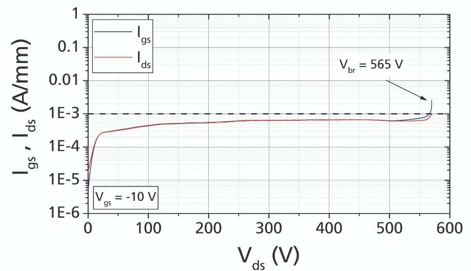
Figure 2. Breakdown voltage measurement of a Fraunhofer IAF 100 V GaN device with a 3.1 mm gate periphery.

Table 1. Load-line resistance, output capacitance and resulting achievable bandwidth (Bode-Fano limit) for -20 dB matching of Fraunhofer IAF’s 50 V and 100 V GaN process, as well as a 100 V GaN process with reduced output capacitance.
As all engineers know, there is no such thing as a free lunch. When the supply voltage increases, devices must withstand higher peak voltages, which occur under dynamic drive. To provide sufficient voltage robustness, engineers must ensure that the breakdown voltages of the RF devices that they employ are at least three-to-four times that of the operational voltage. So, for a device that is to deliver a reliable operation at 100 V, the breakdown should be in the 300 V to 400 V range. That’s not that far from the territory occupied by GaN devices designed for power electronics. However, those devices exhibit comparably large capacitances, limiting the suitable frequency range to just a few tens of megahertz. It is clear that the primary challenge when developing a 100 V GaN technology is to marry a high breakdown voltage with a suitable RF performance for the gigahertz range.
The key to increasing the breakdown voltage is to ensure appropriate control of the peak electrical field in the channel region while preventing the introduction of additional capacitances, which deteriorate RF performance. One possible measure is to increase the gate-to-drain spacing of the transistor. But this has major downsides – it increases the on-resistance of the device, and degrades its achievable output power density and maximum efficiency.
Our team at the Fraunhofer Institute for Applied Solid State Physics IAF is pursuing a more holistic approach, based on the combination of an increase in gate-to-drain spacing and optimisation of the source-terminated field plate. Efforts are directed at finding the best combination of breakdown voltage, on-resistance and output capacitance. As a high-voltage operation threatens to impair the long-term reliability of the device, from quite early in our development phase, we have been paying much attention to the origin of degradation mechanisms.
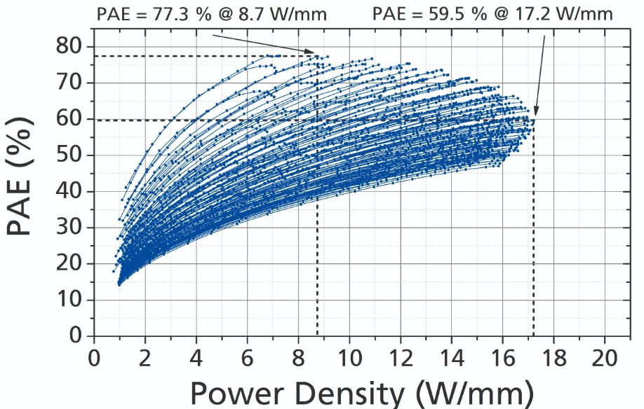
Figure 3. Pulsed 1.0 GHz load pull performance tests on a Fraunhofer IAF 100 V GaN device with 3.1 mm of gate periphery. Second and third harmonic output impedances have been terminated for maximum efficiency. Pulse width was set to 10 μs with a duty cycle of 10 percent.
One option for increasing the breakdown voltage is to extend the source-terminated field plate further towards the drain electrode, as this quashes the peak electrical field at the gate edge. The price to pay is an additional capacitance against the drain-side part of the channel. This manifests itself as additional output capacitance. For efficiency reasons, this additional extension of the field plate compared with a lower-voltage device should be kept as small as possible.
Usually, when an engineer designs a high-efficiency amplifier, they exploit a technique known as ‘harmonic termination’. Rather than matching just the fundamental frequency, they also use matching networks with specific impedances for the second and third harmonic frequencies – and sometimes even higher ones too. By taking this approach, they can design amplifiers operating in the likes of a Class-E, Class-F or Class-F-1 configuration that have a theoretical maximum efficiency of 100 percent. In comparison, the theoretical maximum for class B, involving shorting all harmonics, is just 78.5 percent.
When considering the behaviour of the HEMT, its helpful to think about the equivalent circuit. This is the combination of a load-line resistance and output capacitance that form a shunt RC-circuit. At high frequencies, the output capacitance dominates the output impedance of the transistor, resulting in a quasi-short-circuit. So, the higher the selected fundamental frequency, the greater the number of harmonics that tend to be intrinsically shorted by the presence of the output capacitance. This forces the device into a Class-B-like operation, limiting the theoretically achievable efficiency. To avoid this limitation and get the full benefit from the efficiency enhancement that harmonic termination brings, it is critical to ensure that the output capacitance is as small as possible.
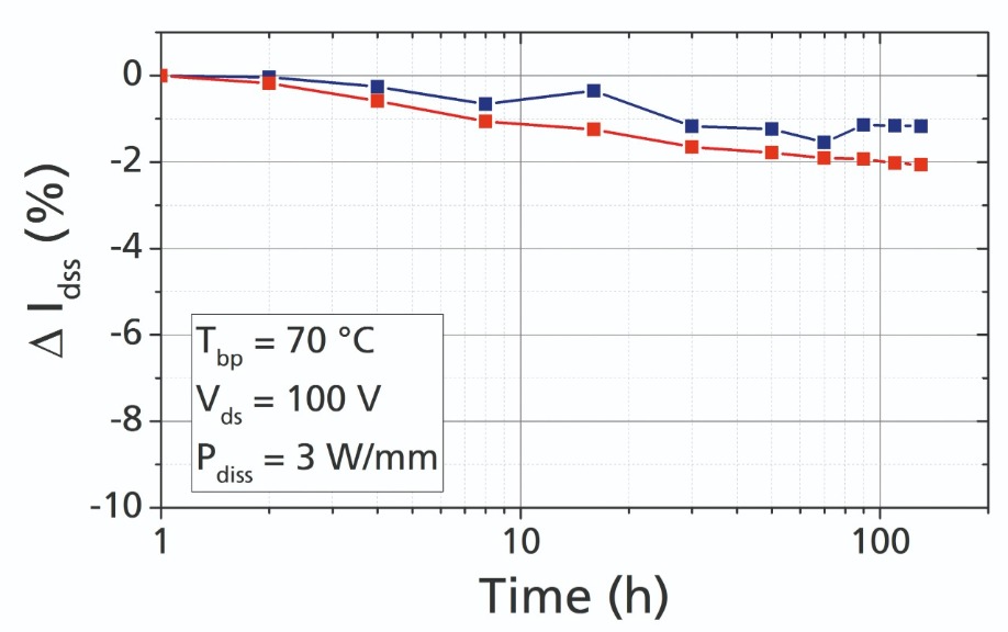
Figure 4. DC high-temperature operation lifetime results at a drain-source voltage of 100 V and a dissipated power of 3 W/mm of gate periphery. The baseplate temperature was set to 70 °C, resulting in a simulated junction temperature of 150 °C.
When designing an amplifier, one must note that the achievable bandwidth is inversely proportional to the product of load-line resistance and output capacitance – this is an outcome of the so-called Bode-Fano criterion. For example, if the load-line resistance doubles, the maximum achievable bandwidth halves. Note that the same relationship holds for a respective increase in output capacitance.
In principle, when the achievable bandwidth is lower, the network has to be more complex to match a given bandwidth. As stated before, a higher load-line resistance allows the use of simpler matching networks. However, this only holds when the achievable bandwidth is maintained. Consequently, the goal of the designer is to trim the overall output capacitance, so that this compensates for the higher load-line resistance caused by operation at a higher supply voltage.
Although a source-terminated field plate helps to reduce the peak electrical field in the channel, if it is poorly designed, it can impair device performance. As discussed already, when a source-terminated field plate is added, it creates an additional parasitic output capacitance. As the extra capacitance is detrimental to both the achievable efficiency and the matching bandwidth, it must be designed with much care.
Producing high powers
Building on our baseline 50 V GaN technology, we have developed a 0.50 μm gate length AlGaN/GaN-on-SiC technology for 100 V operation. We have used this to make our devices that feature a dual field plate configuration and individual vias in each source region. Thanks to the high power density of this process, output powers can exceed 500 W per single transistor die. To cope with the high dissipation associated with operation at elevated supply voltages, we have used finite element modelling to optimise all layouts.
Based on all the considerations that we have discussed here, such as the gate-drain distance and the insertion of the source-terminated field plate, we have developed our transistor technology to co-optimise efficiency and breakdown voltage. Initially, our efforts focused on L-band frequencies (1 GHz – 2 GHz), but we are now working to extend the usable frequency range beyond 6 GHz. Our view is that a well-engineered 100 V technology could feature capacitance values – such as those for the gate-source, gate-drain, and drain-source – that are comparable with those of established 50 V technologies. Succeed on this front and our 100 V devices should be able to serve a similar frequency range.
Measurements of the DC performance of our 50 μm single-gate-finger device reveal a maximum transconductance of more than 280 mS/mm at a 10 V drain-source voltage. We selected a gate length of 0.50 μm to minimise short-channel effects. Its success is proven by a very low drain-induced barrier lowering – it is below 5 mV/V.
We have undertaken further characterisation of our technology using a larger device, which has a periphery of 3.1 mm. By finding an optimum combination of extended gate-drain distance and geometry of the source-terminated field plate, we have trimmed the on-resistance to just 5.0 Ω mm. What’s very encouraging is that this device has a gate-drain breakdown voltage exceeding 550 V, without any evident buffer leakage current. We can benchmark this device by considering its ratio of breakdown voltage and on-resistance. It has a figure-of-merit of 110 V / (Ω mm), which is around 50 percent higher than that demonstrated by previous 100 V GaN technologies.
To assess power performance and maximum efficiency of our technology, we have used this device for RF load pull measurements. For this evaluation, made at a frequency of 1.0 GHz, we terminated the second and third harmonic impedances to ensure maximum efficiency. Tests reveal a maximum power density of around 17.2 W/mm and a power-added efficiency of 77.3 percent, based on load pull measurements of 169 different fundamental impedances. Our power-added efficiency at L-band frequencies is the highest value that has ever been reported for a 100 V GaN technology.
In addition to a high level of performance, RF devices need to deliver good reliability under elevated temperatures to serve in high-power systems. To gain some insight into the long-term stability of our technology, we have performed DC high-temperature accelerated lifetime tests on two of our 3.1 mm devices, which we mounted onto a 1 mm-thick copper-molybdenum-copper carrier. We found that after 130 hours of stress at an estimated junction temperature of 150 °C the saturation drain current fell by just 2 percent, demonstrating the basic reliability of our 100 V technology. We are now undertaking a more thorough reliability investigation at higher junction temperatures.
Our measurements provide an insight of what it should be possible to achieve with a 100 V GaN technology. We are now building on our record-breaking efficiency at L-band frequencies, with efforts directed at extending the applicable frequency range towards the C-band (4 GHz – 6 GHz), and even beyond. To succeed, we will need to further reduce our output capacitance. Do this and our efficiency will increase even more, particularly at high frequencies. An additional, associated benefit will be an increase in achievable bandwidth, leading to high-bandwidth, high-power designs.
Based on the progress we have made, we have every reason to believe that our 100 V technology will extend the limits of what can be realised with this wide bandgap technology.
S. Krause et al. “High-Power-Density AlGaN/GaN Technology for 100-V Operation at L-Band Frequencies,” 2019 IEEE International Electron Devices Meeting (IEDM), San Francisco, CA, USA, 2019, pp. 17.4.1-17.4.4.
G. F. Formicone IEEE Trans. Semicond. Manuf. 31 440 (2018)
R. Leoni et al. “Raytheon high power density GaN technology,” 2017 IEEE Compound Semiconductor Integrated Circuit Symposium (CSICS), Miami, FL, 2017, pp. 1-4.

HEMTs and filters are set to benefit from high-quality ScAlN
A team from the University of Michigan claims to have produced high-quality films of ScAlN with a higher scandium content than ever before, and used them to provide new insights into the bandgap and refractive index of this alloy.
This work is of much value, because ScAlN is piquing the interest of the compound semiconductor community, due to its unique ferroelectric and large spontaneous polarisation. These attributes promise to improve the performance of surface acoustic wave resonators and HEMTs, devices that can be deployed in combustion engines, smart vehicles and 5G technologies.
The team has used MBE to produce a range of epitaxial films with a scandium content of up to Sc0.34Al0.66N. All these films combine smooth surface morphology – values for the root-mean-square roughness below 1 nm – with excellent crystal quality. According to X-ray diffraction measurements, the peaks associated with differing compositions of this alloy have a rocking curve full-width at half maximum for the (002) plane of below 450 arc sec.
Note that although it is possible to crank the scandium content up to even higher values by sputtering, poor crystal quality results, leading to a dramatic decrease in the piezoelectric coefficient.
Another breakthrough by the researchers has been establishing a linear relationship between the bandgap of ScAlN and its composition. The formula put forward by the team, which is in good agreement with a previous theoretical prediction, differs from other experimental reports that underestimate the bandgap, due to mixed phases and a high density of defects.
According to Michigan’s spokesman Ping Wang, this finding provides an additional dimension to engineer the bandgap of III-nitrides, and paves the way to the fabrication of ScxAl1-xN based optoelectronic and photonic devices.
Wang says that their latest paper also provides the first report of the monotonically tuneable refractive index between AlN and GaN.He believes that the refractive index of ScAlN, which varies significantly with composition, could aid designers of high-performance III-nitride photonic integrated circuits and optical cavities, as they could engineer this novel alloy for deep ultraviolet and visible waveguides and lattice-matched distributed Bragg reflectors.
By turning to MBE for the growth of ScAlN, Wang and colleagues can use commercially available scandium metal as a source. In comparison MOCVD, the other common growth technology for compound semiconductor films, requires the use of highly complicated synthetic routes to produce a source for scandium.
Impurities are also an issue with MOCVD. They come from the metal-organic sources and the chamber atmosphere. MBE, in comparison, inherently limits incorporation of undesirable impurities, such as carbon and oxygen, thanks to growth in an ultra-high vacuum.
Yet another advantage for MBE over MOCVD is its capability at the low temperatures required to realise scandium-rich alloys. “Generally, low growth temperature will lead to a low cracking efficiency for precursors in MOCVD, and further deteriorate the epitaxy process,” argues Wang.
One of the goals for the team is to demonstrate ferroelectric switching – this has already been reported for polycrystalline ScAlN. “The pure wurtzite phase can further enhance the ferroelectric performance due to uniform crystal orientation,” says Wang
Additional objectives include increasing the composition of scandium in ScAlN – theoretically, stable films are possible up to a composition of Sc0.55Al0.45N – and addressing the impurities in these alloys, which predominantly come from the scandium source.
Efforts will also be directed at devices. The team have already produced ScAlN/GaN HEMTs, which require evaluation, and they plan to design and make deep UV and visible ScAlN LEDs.
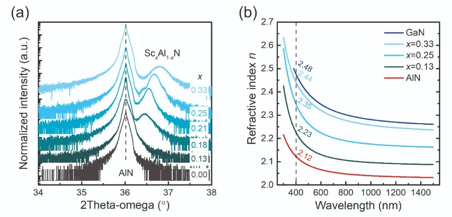
(a) (002) plane X-ray diffraction and (b) refractive index versus wavelength for various compositions of ScxAl1-xN.
P. Wang et al. Appl. Phys. Lett. 116 151903 (2020)

Freeing films created by lateral layer overgrowth yields small semi-polar substrates
ProducING high-performance, semi-polar devices is thwarted by the incredibly high cost and limited availability of accompanying substrates. But this barrier could be overcome, according to a team from the University of California, Santa Barbara, that is pioneering a lower-cost technology that is capable of producing small bars of semi-polar material.
The researchers make more affordable material by cleaving films that are grown on patterned semi-polar substrates, which can be re-used. The resulting material, created by epitaxial layer overgrowth and having lateral dimensions of tens of microns, could form the foundation for semi-polar microLEDs.
Team spokesman Srinivas Gandrothula told Compound Semiconductor that he and his co-workers have been working on this project for more than three years, with efforts directed at producing both semi-polar and non-polar bars. Success with the later led to a claim for the first functional, thin-film, edge-emitting laser, reported in 2019. As it is not possible to grow high-quality indium-rich epilayers on non-polar planes, the work recently diversified to include the fabrication of semi-polar bars.
Gandrothula argues that one of the merits of the team’s technology is that it “forgives” the randomness of the dislocations in the parent substrate. In addition, it is claimed to enable superior thermal management, thanks to the use of thin epitaxial device layers that are isolated from the thick parent substrate.
To pick devices from the substrate, the team uses commercialised dicing tape. “This technique can claim 100 percent yield by repeating the process several times on the same device-containing wafers,” says Gandrothula.
For the team’s semi-polar work, the starting point is a portfolio of free-standing substrates with angles of ± 10 °, ± 15 °, and ± 28 ° to the m-plane – they are the semi-polar planes (101M1), (2021) and (3031), and their complimentary planes. On these foundations, Gandrothula and co-workers deposit a 200 nm-thick SiO2 dielectric layer, before using HF acid to open a series of rectangular stripes, typically 20 μm wide and 1.2 mm in length. These openings have breadthwise pitch of 80 μm and a lengthwise pitch of 1.3 mm.
The patterned substrates are loaded into an MOCVD chamber, where thick layers of GaN are grown epitaxially from selectively opened windows. After 4 hours, films are formed with a thickness of more than 10 μm. Note that growth ceases prior to coalescense with epitaxial layers from neighbouring windows.
Inspecting films with a scanning electron microscope revealed that as the inclination from the m-plane increases, so does the top width (see figure).
To separate the films from the substrate, Gandrothula and co-workers begin by removing the dielectric mask with HF acid and placing and firmly pressing commercial dicing tape on the GaN bars. Rapid immersion in liquid nitrogen follows, with the sample containing the tape left in the liquid for a minute or two, before warming it to room temperature with nitrogen gas. After this, when the tape is slowly peeled off, the epitaxial films separate from the growth substrate.
The researchers had a 100 percent yield for bar removal when the window width was below 10 μm. When this is increased yield falls, dropping to 60 percent for a 20 μm-wide window.
As well as need to address this issue, the team must prevent craters with a depth of up to 3 μm from forming when the bar is removed from the windows. Another goal for the team is to develop large size semi-polar and non-polar GaN substrates by tiling the removed epitaxial layers. “Due to limited resources, we are looking to collaborate with substrate manufacturers on this project,” says Gandrothula.
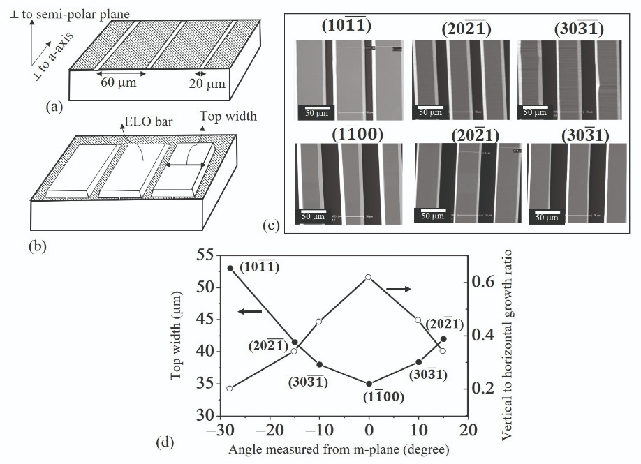
Creating windows in a mask on a semi-polar substrate (a) allows the growth of semi-polar material (b). Growth rates depend on the semi-polar orientation.
S. Gandrothula et al. Appl. Phys. Express 13 041003 (2020)

Trenches prevent on-off ratios plummeting at elevated temperatures
Engineers from the University of Michigan have revealed that trenches enhance the performance of β-Ga2O3 Schottky barrier diodes at elevated temperatures. This architecture will help the deployment of these diodes in harsh environments.
Power devices made from β-Ga2O3 are attracting much attention, due to an ultra-wide bandgap that enables very efficient switching and the promise of low-cost substrate production by melt-growth techniques. Unfortunately, realising p-type doping is not possible, so developers of diodes are avoiding p-n junctions and pursuing devices with a Schottky barrier.
Armed with a trench, β-Ga2O3 Schottky barrier diodes can produce an on-off current ratio as high as 105 at a temperature of 650K, a value of four orders of magnitude higher than that provided by a conventional design.
The addition of the trench also enhances robustness. After high-temperatures measurements, the current-voltage characteristics of this device recover, while those for the standard Schottky barrier diode are permanently degraded.
Fabrication of the diodes began by loading n-type β-Ga2O3 (001) bulk substrates into a HVPE chamber, and depositing a 10 μm-thick, n-type layer.
After dicing the wafer into 1 cm by 1 cm pieces, etching the backside and evaporating 20 nm of titanium and 200 nm of gold produced a good ohmic contact.
Depositing 20 nm of nickel and 100 nm of platinum on the front surface followed. This provided the Schottky contact, and, after patterning, a hard mask for trench formation. Inductively coupled plasma etching defined 1.3 μm-deep trenches, before soaking the wafer in hydrochloric acid for 10 minutes removed etch damage.
Using this approach, the team produced a portfolio of diodes along the [010] and [100] directions. Devices were made with fin widths of 1 mm, 2 mm, 3 mm and 4 mm and fin area ratios of 20 percent, 35 percent and 50 percent. To complete the fabrication of the devices, the engineers added: a 100 nm-thick layer of Al2O3 by atomic layer deposition; used a photoresists planarization process to remove this dielectric from the top of the ridges, and add Ni/Pt; and sputtered 10 nm of titanium and 300 nm of chromium on the sidewalls.
Measurements revealed that the Schottky barrier diodes with trenches in the [010] direction had better electrical characteristics than those with trenches in the [100] direction. Superiorities included a lower on-resistance and better current-voltage characteristics.
Based on these findings, the engineers restricted further evaluation to Schottky barrier diodes with trenches in the [010] direction. Testing these diodes showed that compared with conventional counterparts, the turn-on voltage is higher by 0.16 V. This slightly higher value is attributed to sidewall depletion, caused by the adjacent metal-oxide-semiconductor junction on the sidewalls of the trench.
The researchers have found that the on-resistance of the Schottky barrier diodes is at least twice that of similar trench-based devices reported by another group. This is said to be partly due to a lack of annealing of the Ohmic contact, and partly due to creating a contact pad from sputtered chromium – it has a far higher resistivity than gold.
Room-temperature measurements reveal on-off ratios of 1010 for conventional and trench-based Schottky barrier diodes. For those with a trench, leakage current remains under the detection limit at temperatures of up to 550 K, while for conventional cousins, detectable leakage kicks in at 350 K. This leakage increases with temperature, and is to blame for an on-off ratio of just 10 at 650 K.
Formation of defects in the material is thought to be behind the inferior performance. The researchers are planning to investigate this by testing the hypothesis that the proximal trench sidewall acts as a sink for defects.
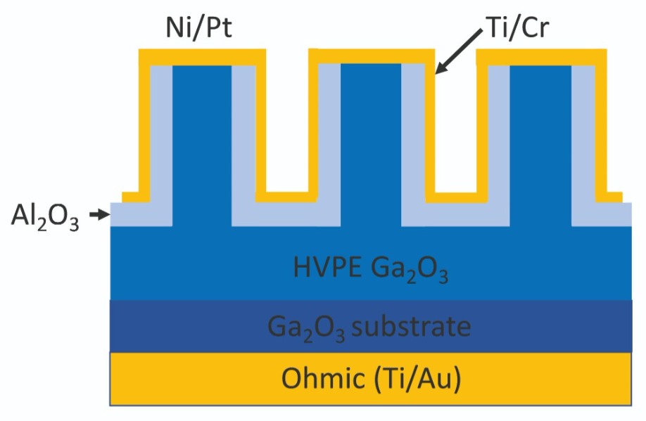
Trenches improve the high-temperature performance of b-Ga2O3 Schottky barrier diodes.
Z. Jian et al. Appl. Phys. Lett. 116 152104 (2020)
