




THE COVID-19 epidemic is having a massive, global impact. It has already claimed tens of thousands of lives and forced many of us to adhere to a variety of social distancing measures, such as working from home and only leaving the house for essentials.
Until this epidemic is brought under control, it is unthinkable to host a global conference. It is for that reason that CS International has been rescheduled for November – although, to maintain communication and the flow of information within our community, we are also hosting a free, online summit on Tuesday 19 May.
A report on CS International would often be found within the pages of the April & May edition. But due to its absence this year for the reasons just outlined, there is more space in this issue to devote to a particular technology. And as you’ll see, here you’ll find detailed coverage of the development of the GaN IC.
The tremendous attributes of GaN and its related alloys – such as its ability to withstand high electric fields, its high saturation velocity that aids high-frequency operation, and its low on-resistance that leads to low switching losses – are driving its deployment in power electronics, communication and radar.
However, GaN has its weaknesses. High-performance p-type GaN FETs are challenging to produce, hampering the development of a GaN CMOS technology that will allow GaN power transistors to switch at far higher frequencies. Addressing this issue is critical, as it will allow circuit efficiency to increase in power supplies, while slashing the size and weight of passive components.
Offering one route to realising these gains are a team at MIT that has developed aggressively scaled FETs that feature a two-dimensional hole gas to provide carriers.
Working with this team, and a group at Cornell, are researchers at Intel. They reason that a good stepping stone to an all GaN CMOS technology is to unite GaN NMOS with high-k metal gate silicon PMOS. To accomplish this, they stack GaN and silicon transistors on 300 mm silicon wafers using a three-dimensional layer transfer process.
At imec, the microelectronics research centre in Belgium, they are adopting a different approach to making a p-FET. Rather than tackling the problem head-on, they are turning to a single-transistor invertor with a resistive load. Another feature of their work is the use of a buried oxide layer on a silicon-on-insulator substrate to ensure electrical isolation between different modules.
I encourage you to read about this breakthroughs at imec, plus those at Intel and MIT, while also participating in our on-line summit. As well as the insight you’ll gain, it could play a part in helping you to feel connected during this outbreak.
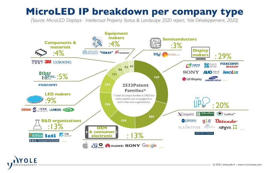
IN YOLE’S latest microLED display report, its analysts estimate that the cumulated effort in microLEDs to date reaches close to $4.8 billion, with Apple alone close to $1.8 billion, factoring in both the Luxvue acquisition and internal developments.
Excluding this acquisition and the recent deal between Facebook and Plessey, start-ups have raised a cumulated $800 million to date and could add another $100 million in 2020 pending disruption due to the Covid-19 pandemic. In addition, panel makers such as Samsung, LG, AUO and Innolux also significantly increased their efforts.
“The growth is fuelled by the meteoric rise of Chinese companies”, asserts Eric Virey, principal display market and technologies analyst within the Photonics, Sensing & Display division at Yole Développement.“This mirrors a more general trend in the country as it transitions from a manufacturing to an innovation driven-economy. This also reflects the situation in the display industry where Chinese companies now hold more than 50 percent of the worldwide display capacity in 2020.”
About 5,500 patents filed by more than 350 organisations and representing almost 2,500 families have been identified and selected by Yole. The level of activity is growing exponentially with 40 percent of the patents filed in 2019 alone.
“The increase in patents coming from China is remarkable”, comments Virey. “Many of those microLED patents are questionable. Nevertheless, established players shouldn’t underestimate their Chinese competitors and dismiss the threat: some patents show world-class innovation and demonstrate a strong resolve to close the gap with established rivals.” In addition, in high volumes, even low-quality patents can be used as bargaining tools to fend off infringement lawsuits, negotiate cross licensing agreements and so on.
The proliferation of sub-par patents may however hinder innovation as it increases barriers to entry: increasing resources are required to conduct freedom-to-operate analysis, monitor patent activities, try to invalidate wrongly granted patents and respond to infringement lawsuits.
Over the last two years, the industry has entered what can be seen either as a virtuous cycle or a bubble: companies are jumping on the microLED bandwagon for fear of being left out.
Virey explains: “Display makers dominated IP activity in 2019. Most were initially dismissive of microLEDs, but all are now accelerating their effort. BOE now leads in volume with close to 150 new patent families in 2019 alone.”
LG, AUO, Samsung, CSOT, Tianma, Innolux, CEC Panda, Visionox and companies in the Foxconn group all dramatically increased activity as well.
Korean firms are investing massively in OLEDs but microLEDs could be a credible alternative for high-end TVs. Chinese makers are at least three years behind Korea in OLEDs, so microLEDs could be a more differentiating play. For companies such as AUO or Innolux that haven’t invested in OLEDs, microLEDs could be critical for long-term survival and allow them to remain relevant in various high-end market segments without requiring OLED-like multi-billion dollar capex.
Many companies now have portfolio addressing multiple technology nodes. Licensing and legal battles will likely arise if microLED displays enter volume manufacturing. Except in the field of microdisplays where the most capex-intensive manufacturing steps can easily be outsourced, start-ups and small companies are not planning to become display makers. Rather, most will focus on their core expertise and attempt to license their technology to established display makers and OEMs.
In order to compete with LG’s white OLED and maintain its leadership in the high TV market segment, Samsung Display Company announced a $13 billion investment to develop and manufacture QD-OLEDs by 2021-2022. But Samsung is hedging its bets: its Visual Display group is developing microLEDs using in house mass transfer and chips developed by Playnitride.
Surprisingly, activity at Apple has slowed significantly since 2017. The few patents it has since published, however, show the high level of maturity and advancement reached by the company in microLED display technologies. Recent patents also show that the company has expanded the scope of its effort into developing microdisplays for augmented reality. Overall, the reduced activity could also be a sign of confidence in an already robust microLED portfolio as the company now focuses on setting up its supply chain. If successful, Apple would be the first to disrupt the industry by having developed its own display technology and establishing a mostly fabless supply chain model, something that Huawei could be willing to emulate.
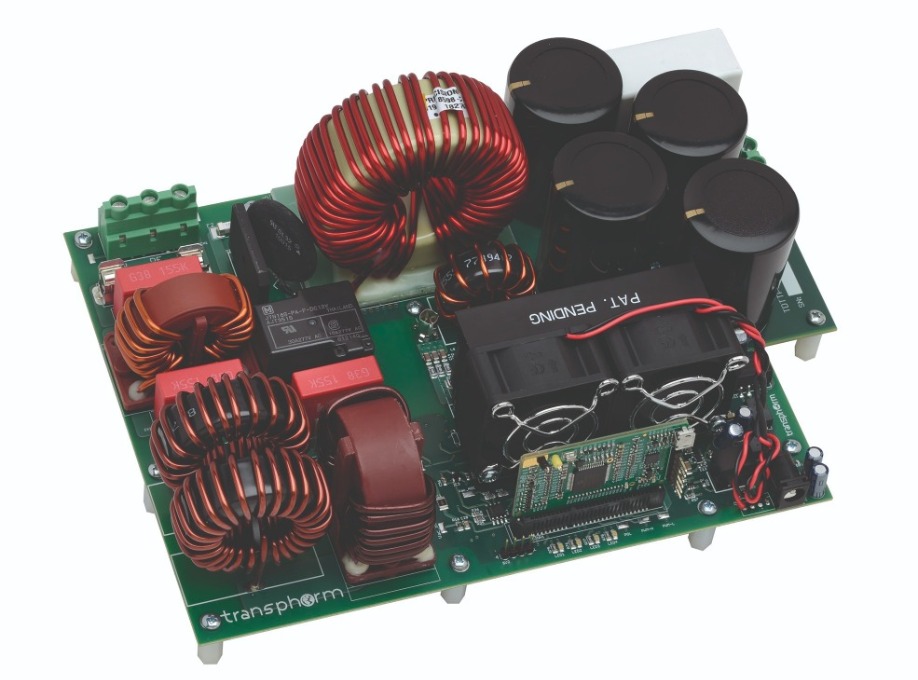
TRANSPHORM has announced that it has partnered with microcontroller provider Microchip Technology to integrate a Microchip dsPIC33CK digital signal controller board with Transphorm’s 4 kW AC-to-DC bridgeless totem power factor correction (PFC) GaN evaluation board.
Building on Transphorm’s application support capabilities, Microchip’s worldwide technical support team will also be available to developers working with the integrated Transphorm solution.
As a result, customers can access an evaluation board offering more than 99 percent efficiency and pre-programmed firmware off the shelf, now backed with global support to further simplify AC-to-DC power system designs.
“Transphorm’s Microchip collaboration is a gamechanger,” said Philip Zuk, VP of Worldwide Technical Marketing and North American Sales, Transphorm. “The control requirements of GaN power systems using the bridgeless totem-pole power factor correction is different than what is used to control traditional CCM boost PFCs, which has long been a new challenge for some ODMs. Today, two industry leaders have partnered to reduce that knowledge gap. We’re giving customers access to a disruptive GaN solution backed by a world-class global support team.”
Microchip’s dsPIC Digital Signal Controllers (DSCs) are supported by a set of embedded design tools created to empower developers, even those with limited expertise. These tools provide intuitive graphic user interfaces for device initialisation in Microchip’s free MPLAB X Integrated Development Environment. The software tools are complemented by a full line of programmer, debugger and emulator accessories.
“Microchip’s dsPIC DSCs are designed to meet the demanding control needs associated with newer digital power topologies,” said Joe Thomsen, VP of MCU16, Microchip. “We are proud to work alongside a likeminded industry disruptor, Transphorm, to provide our customers this reference design including Transphorm’s proven GaN devices. Our dsPIC33CK PIMs will offer engineers the flexibility and worldwide support that many designers need for their high-power solutions.”
REVENUE from RF GaAs-enabled devices fell by nearly 6 percent in 2019, marking the biggest decline since 2004. The Strategy Analytics Advanced Semiconductor Applications (ASA) report RF GaAs Device Industry Forecast: 2018 - 2024 identifies declining smartphone shipments as the primary culprit for this drop in GaAs revenue.
The report does go on to forecast that growth will resume, allowing RF GaAs device revenue to approach $9 billion by 2024. Drivers for this renewed growth will be the quickening pace of 5G network and device deployments.
“Wireless applications, particularly cellular terminals, dominate GaAs device revenue,” noted Eric Higham director of the Advanced Semiconductor Applications (ASA) service. “Smartphones contain substantial GaAs content, so it was no surprise when declining shipments in 2019 pulled down the entire GaAs market.”
He went on to say, “Despite the uncertain Covid-19 implications, I remain optimistic that expanding deployments of 5G devices and networks will become the new growth engine for GaAs device revenue. We will be monitoring developments at GaAs handset PA manufacturers like Skyworks, Qorvo and Broadcom to get better clarity about the 5G growth trajectory.”
AXT, a manufacturer of compound semiconductor substrates, has announced that one of its largest GaAs wafer substrate customers has formally qualified the company’s new GaAs substrate processing facilities.
“Among the customers now qualified on the new GaAs manufacturing line, we are pleased to announce that one of our largest GaAs customers has qualified our new manufacturing sites for volume production,” said Morris Young, chief executive officer. “This Tier-1 customer has among the highest quality, safety and environmental standards in its industry. Its confirmation is an important milestone for AXT’s manufacturing relocation, and will enable us to meaningfully ramp production from our new locations to meet our customers’ needs over the coming quarters.”
During the fourth quarter of 2019, AXT transferred its GaAs crystal growth ingot production to its new manufacturing facility in Kazuo, a city approximately 250 miles from Beijing. Wafer processing for GaAs was relocated to its new manufacturing facility in Dingxing, a city approximately 75 miles from Beijing. AXT began offering wafers from Dingxing for customer qualification in 2019, and began customer site qualifications later that year.
“Our new manufacturing sites are optimised for best-practice manufacturing techniques, and we have installed
state-of-the-art equipment. Both are designed to meet and exceed the current rigorous safety and environmental standards in China,” Young continued.
“We now have capacity in place to meet today’s demand for a wide variety of high-end applications, with ample space to expand as demand increases and new applications come to market. I am proud of the teamwork and dedication of our entire AXT team, making this significant accomplishment possible. We are now well positioned to push our technology to new levels of performance required by current emerging applications, and to engage the marketplace with confidence and enthusiasm.”
AXT began manufacturing its GaAs substrate wafers in the Tongzhou district of Beijing, China in 2000. In 2015, the Beijing city government selected Tongzhou for its new municipal headquarters.
Along with many other businesses asked to relocate their manufacturing lines in order to create room and upgrade the district, AXT was instructed to relocate its GaAs manufacturing line.
AQUISENSE TECHNOLOGIES, a US-based maker of UV LED disinfection technology, has launched the PearlSurface 24G9, one of the first UV-C LED surface disinfection products designed for health care applications such as reuse of N95 face masks and other PPE.
The PearlSurface 24G9 offers advanced benefits specific to LEDs, including mercury-free lamps, instant-on operation and a low cost-of-ownership, while providing high-power density, homogeneous disinfection of target objects.
According to the company, the PearlSurface 24G9 offers simple operation, an integrated timer, a low voltage power supply and a compact footprint, making it suitable for point-of-use hospital settings, care homes, ambulances, police/fire departments, factories, food preparation, and so on. AquiSense says it will offer this product under the current US FDA enforcement relief to deal with immediate Covid-19 emergency use and will simultaneously submit a pre-market approval application.
“We accelerated our product development pipeline in response to immediate global needs for reliable reuse disinfection products,” said Oliver Lawal, CEO at AquiSense Technologies.
“We are fortunate to be able to leverage an existing high-output UV-C LED module from our water treatment products and draw on our experience in rapid hardware design and optical modeling to ensure a high-level disinfection efficacy.” concluded Lawal.
AquiSense Technologies is interested in talking to potential partners and distributors for the PearlSurface 24G9.
CREE has announced the expansion of its product portfolio with the release of the Wolfspeed 650 V SiC MOSFETs, delivering a wider range of industrial applications and enabling the next generation of Electric Vehicle (EV) onboard charging, data centers, and other renewable systems with industry-leading power efficiency.
“Cree is leading the global transition from silicon to silicon carbide, and our new 650 V MOSFET family is the next step in delivering a high-powered solution to a broader application base, including industrial applications everywhere,” said Cengiz Balkas, senior vice president and general manager of Wolfspeed. “The 650 V MOSFETs deliver power efficiencies that help today’s biggest technology leaders create the next generation of onboard EV charging, data centers, and energy storage solutions to reshape our cloud and renewable energy infrastructures.”
The new 15 mΩ and 60 mΩ 650 V devices, which use Cree’s industry-leading, third-generation C3M MOSFET technology, deliver up to 20 percent lower switching losses than competing SiC MOSFETs and provide the lowest on-state resistances for higher efficiency and power dense solutions. End users benefit from lower total cost of ownership in a variety of applications through the more efficient use of power, reduced cooling requirements, and industry-leading reliability.
Compared to silicon, Wolfspeed’s new 650 V SiC MOSFETs deliver 75 percent lower switching losses and a 50 percent decrease in conduction losses which results in a potential 300 percent increase in power density.
It is claimed that design engineers can now meet and exceed the industry’s most ambitious efficiency standards, including 80 Plus Titanium requirements for server power.
The new 650 V MOSFET family is also said to be ideal for on-board chargers (OBCs) in the electric vehicle (EV) market. The increased efficiencies and faster switching allow customers to design smaller solutions with added performance. Wolfspeed’s 650 V SiC MOSFETs also enable bi-directionality in OBCs without compromising the size, weight and complexity of the solution. Furthermore, Wolfspeed’s experience with automotive AEC-Q101 qualification, proven in the E-series MOSFET family, paves the way for future automotive qualified 650 V MOSFETs.
Other industrial applications, such as general-purpose switched mode power supplies (SMPS), will also be able to take advantage of the many benefits of the new 650 V SiC MOSFETs from the largest, global and vertically integrated supplier of SiC technologies.
A TEAM from the Technical University of Eindhoven (TU/e) and the Technical University of Munich (TUM) has now succeeded in developing light-emitting, silicon-germanium alloys. As a result, the development of a silicon laser capable of integration into today’s chips is within reach for the first time.
For the past half century, researchers have tried in vain to build silicon or germanium-based lasers. Silicon normally crystallises in a cubic crystal lattice. In this form it is not suitable for converting electrons into light.
Together with colleagues from the Technical University of Munich and the universities in Jena and Linz, researchers at the Technical University of Eindhoven have now developed alloys made of germanium and silicon capable of emitting light. The crucial step was the ability to produce germanium and alloys from germanium and silicon with a hexagonal crystal lattice.
“This material has a direct band gap, and can therefore emit light itself,” says Jonathan Finley, professor of Semiconductor Quantum Nanosystems at TUM.
Erik Bakkers and his team at TU Eindhoven first produced hexagonal silicon back in 2015. They started by growing a hexagonal crystal structure with nanowires made of another material. This served as a template for a germanium-silicon shell on which the underlying material imposed its hexagonal crystal structure.
Initially, these structures could not be stimulated to emit light. Through the exchange of ideas with colleagues at the Walter Schottky Institute at the Technical University of Munich, who analysed the optical characteristics with each successive generation, the production process was finally optimised to a grade of perfection where the nanowires were indeed capable of emitting light.
“In the meantime, we have achieved properties almost comparable to InP or GaAs,” says Bakkers.
As a result, it appears to be just a matter of time before a laser made from germanium-silicon alloys and capable of integration into conventional production processes is developed.
“If we can implement on-chip and inter-chip electronic communications by optical means, speeds can be increased by a factor of up to a thousand,” says Jonathan Finley.
“In addition, the direct combination of optics and electronics could drastically reduce the cost of chips for laser-based radar in self-driving cars, chemical sensors for medical diagnostics, and air and food quality measurements.”
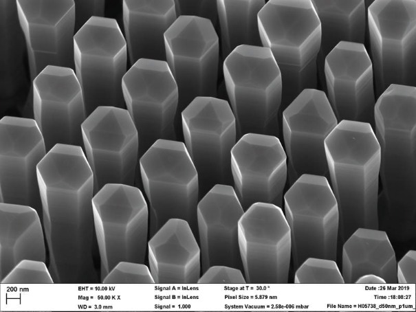
PLESSEY, an embedded technologies developer of microLED technology for augmented and mixed reality (AR/MR) display applications, has announced a new venture.
Plessey will work with Facebook to help achieve their vision of the next computing platform centred around people. Under a new commercial agreement, LED manufacturing operations will be dedicated to helping Facebook prototype and develop new technologies for potential use in the AR/VR space.
With consumer devices like Oculus Quest and a continued legacy of breakthrough research, Facebook is one of the companies best-positioned to make consumer-ready AR glasses a reality.
Plessey share that vision for a future where technology and the barriers between people disappear. Over the last two years, Plessey has been hard at work making the pivot from legacy semiconductor business into microLED’s for AR displays, garnering numerous accolades and industry recognition.
Keith Strickland (Co-CEO/CTO) said “We are delighted to announce this new commercial agreement with Facebook. Plessey has been at the forefront of microLED display development and this agreement recognises the significant advances in our capabilities that we have made in recent years and we very much look forward to working with Facebook to help bring their vision to life.”
Scientists John Geisz (left) and Ryan France (right).
SCIENTISTS at the US National Renewable Energy Laboratory (NREL) have fabricated a solar cell with an efficiency of nearly 50 percent.
The six-junction solar cell now holds the world record for the highest solar conversion efficiency at 47.1 percent, measured under concentrated illumination. A variation of the same cell also set the efficiency record under one-sun illumination at 39.2 percent.
“This device really demonstrates the extraordinary potential of multi-junction solar cells,” said John Geisz, a principal scientist in the High-Efficiency Crystalline Photovoltaics Group at NREL and lead author of a new paper on the record-setting cell.
The paper, Six-junction III-V solar cells with 47.1 percent conversion efficiency under 143 suns concentration appears in the journal Nature Energy. Geisz’s co-authors are NREL scientists Ryan France, Kevin Schulte, Myles Steiner, Andrew Norman, Harvey Guthrey, Matthew Young, Tao Song, and Thomas Moriarty.
Each of the cell’s six junctions is designed to capture light from a specific part of the solar spectrum. The device contains about 140 total layers of various III-V materials to support the performance of these junctions, and yet is three times narrower than a human hair. Due to their highly efficient nature and the cost associated with making them, III-V solar cells are most often used to power satellites, which prize III-V’s unmatched performance.
On Earth, however, the six-junction solar cell is well-suited for use in concentrator photovoltaics, said Ryan France, co-author and a scientist in the III-V Multijunctions Group at NREL.
“One way to reduce cost is to reduce the required area,” he said, “and you can do that by using a mirror to capture the light and focus the light down to a point. Then you can get away with a hundredth or even a thousandth of the material, compared to a flat-plate silicon cell. You use a lot less semiconductor material by concentrating the light. An additional advantage is that the efficiency goes up as you concentrate the light.”
France described the potential for the solar cell to exceed 50 percent efficiency as “actually very achievable”.
Geisz said that currently the main research hurdle to topping 50 percent efficiency is to reduce the resistive barriers inside the cell that impede the flow of current. Meanwhile, he notes that NREL is also heavily engaged in reducing the cost of III-V solar cells, enabling new markets for these highly efficient devices.
LAST YEAR, scientists from Meijo University and the R&D division of Stanley Electric in Japan demonstrated high-efficiency and high-power operation for blue GaN-based VCSELs with AlInN /GaN distributed Bragg reflectors (DBRs). They published the results in Applied Science.
These AlInN /GaN DBRs are used at the front (emitting) side of the VCSEL that emits through the GaN substrate and is completed by a second, dielectric DBR at the VCSEL’s back-side. Hence, perfect lattice match of the AlInN in the front DBR is essential for enabling extremely low-defect InGaN layers in the active zone of the device that is grown on top of the AlInN /GaN DBRs.
Now, the German metrology company Laytec has reported that a paper in the Journal of Crystal Growth by scientists from Meijo University shows the power of its EpiCurve TT metrology tool in revealing and controlling the AlInN strain and alloy compositions at accuracy levels of XRD already during growth of the epitaxial
layers.
The team developed a model for in-situ wafer curvature values of AlInN/GaN DBRs and determined InN mole fractions in the DBRs with the model.
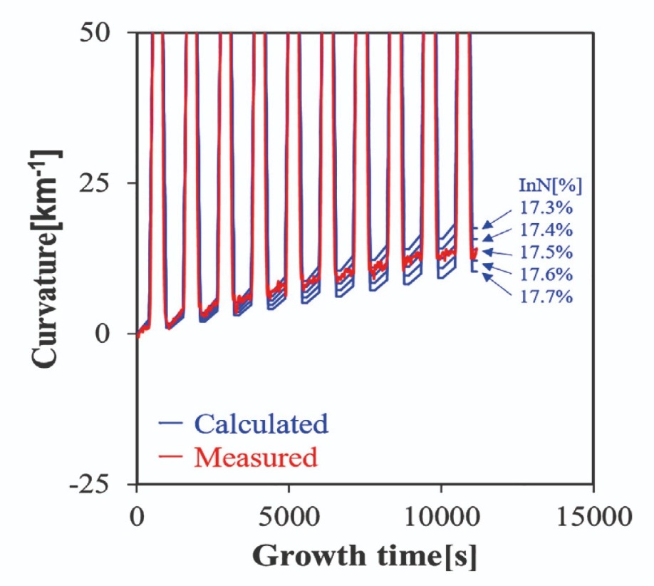
Fig. 1a: Measured in-situ wafer bow of GaN/AlInN DBRs on a GaN substrate as measured (red line) and simulated for several InN mole fractions (blue lines). Shown is a magnified view to the low-temperature (825°C) AlInN wafer curvature sequence.
They found that an increase of curvature changes at the substrate temperature ramping steps was explained by an increase of the total epitaxial layer thicknesses. Another finding was that strain inthe GaN layers at the GaN layer growth steps was almost zero.
Finally, they determined the InN mole fractions in the AlInN layers by using the model, showing excellent agreements with the values estimated from ex-situ X-ray diffraction measurements.
The model reveals not only the entire in-situ curvature change profile but also the InN mole fraction under the precisely lattice-matched condition of AlInN/GaN DBRs.
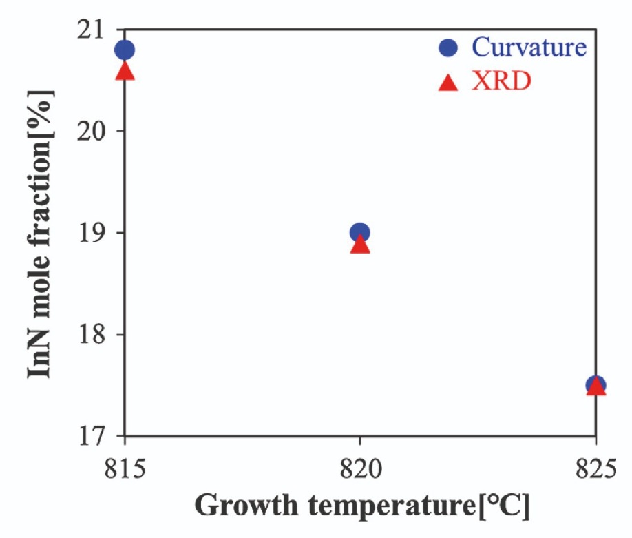
InN mole fraction values estimated from the in-situ curvature measurements and the ex-situ XRD measurements.
UK start-up, Porotech, is set to commercialise porous GaN, opening the door to high-performance optoelectronic devices with unexpected properties, reports Rebecca Pool.
A RELATIVELY UNKNOWN MATERIAL from a newly minted UK start-up is set to make waves in the rapidly growing GaN market.
With a host of novel properties that open the door to high-performance optoelectronic devices, ‘porous GaN’ is attracting more and more interest in compound semiconductor circles. And thanks to £1.5 million in investment funds, University of Cambridge spin-off, Poro Technologies – or Porotech – is on course to be one of the first companies to bring this mesoporous version of GaN to market.
Porous GaN can be regarded as a semiconductor composite of solid GaN and air. As Rachel Oliver, Co-founder and Chief Scientific Officer of Porotech, and Director of the Cambridge Centre for Gallium Nitride puts it: “Porous GaN is basically GaN with holes in it that are a few tens of nanometres across.”
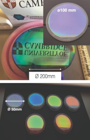
Seed round investment is being used to develop a pilot plant in Cambridge, UK, and Porotech’s first products.
The Porotech team creates the nanoscale porosity in GaN wafers using electrochemical etching. The etch is conductivity selective and responds differently to the material depending on its doping density. Porosity is created in doped layers while undoped layers are left undamaged, allowing complex three-dimensional nanostructures to be created.
According to Oliver, the etchant flows to and from the doped layers via the many nanometre-scale channel-like defects – dislocations – that exist within any GaN wafer.
“Even your best quality GaN wafer will still have around 105 dislocations per square centimetre,” she explains. “So the etchant will flow down a dislocation and when it hits the doped layer will etch it very quickly to create the porosity before continuing down that channel to the next doped layer.”
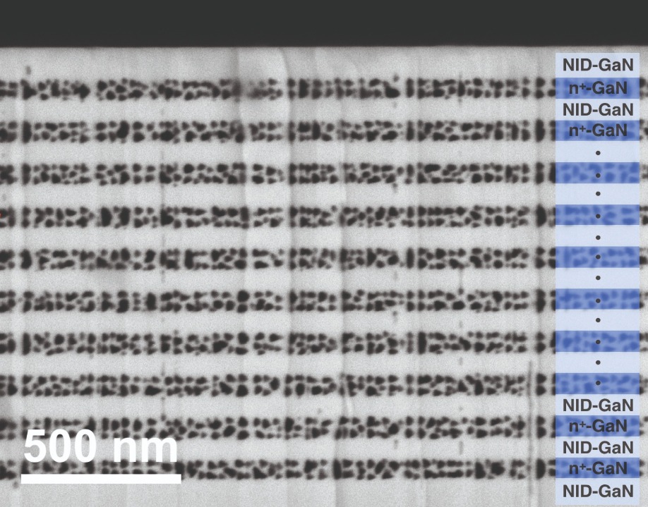
Electrochemical etching provides nanoscale porosity
Indeed, both Oliver and Porotech chief executive and co-founder Tongtong Zhu are certain their porous GaN fabrication process lends itself to commercial exploitation. The method has been tried and tested for wafers up to eight inches in diameter and Zhu reckons it will seamlessly scale to even larger wafer sizes.
“The first thing that inspired us to pursue this process commercially is that it works with wafers,” says Zhu.
“What’s more, during the process we preserve the surface quality and the integrity of the materials so anyone can take the porous GaN wafer and insert it into their production processes without any disruption.”
Devices to go
Oliver, Zhu and colleagues have already fabricated several components and device prototypes. They have demonstrated highly reflective Distributed Bragg Reflectors (DBRs) – or ‘Poro Mirrors’ – based on wafers comprising alternating layers of solid and nanoporous GaN. InGaN LEDs were then grown on these epi-ready DBR pseudo-substrates that were some 25 percent more energy efficient than standard LEDs.
“This DBR substrate is fully compatible with GaN so a customer doesn’t need to process anything differently during LED fabrication, but can still get a brighter and more efficient LED,” points out Zhu.
Porotech has also joined forces with other institutions and start-ups to fabricate thermal sensors that use porous GaN layers as on-chip thermal insulation. And in a novel technology twist, the team has filled the pores in a porous GaN wafer with a halide perovskite to create an optoelectronic material with longer-lasting luminescence.
“These luminescent perovskites are useful in solar cells and LEDs but degrade very quickly,” says Oliver. “We can slow this degradation down with porous GaN.”
Excitingly, novel porous GaN devices could be reaching commercial markets sooner rather than later. Despite the coronavirus pandemic, the Porotech pilot plant is currently being built at Cambridge, and Oliver, Zhu and colleagues are transferring production process from the laboratory to the plant.
“The plant will be operational before June this year and we’re going to start with small-scale production to show that our wafers can be produced in volume,” says Zhu. “We’re currently preparing tens of wafers for customer trials and eventually intend to demonstrate that we can produce thousands of wafers a year.”
The company is also working with foundry services, wafer producers and integrated device manufacturers, and hopes to license out technology in the coming years. “We’ve been working to get the company off the ground for several years and we aren’t going to stop now,” says Oliver. “There has been no other time when GaN is rising so quickly and we have to keep up our momentum.”

Poro Technologies co-founders (left to right): Tongtong Zhu (CEO), Rachel Oliver (CSO), Yingjun Liu (CTO)
Shipments of Oxford Instruments Plasma Technology’s deposition and etch tools are rising, due to their deployment in critical processes used for chip manufacture in growing markets
BY RICHARD STEVENSONHAS THERE EVER BEEN a better time to be working within the compound semiconductor industry? Never before have there been so many emerging markets tipped to generate billions and billions of dollars in device sales. Over the next few years shipments of GaN transistors will underpin the roll-out of 5G infrastructure; SiC transistors and diodes will enhance electric vehicles; GaAs VCSELs will become more common in smartphones and provide a source for other 3D sensing applications; and interest will mushroom in photonic integrated circuits, which can be used for communication and sensing.
All this activity is particularly good news for the makers of processing equipment for the compound semiconductor industry. That includes Oxford Instruments Plasma Technology, a division of Oxford Instruments based in Yatton, just outside Bristol.
According to Managing Director of Plasma Technology, Mike Gansser-Potts, the compound semiconductor market is now entering a high-volume manufacturing phase where the performance it enables is demanded by global trends, such as efficient energy and driverless vehicles.
Plasma Technology is in a particularly strong position to make the most of these opportunities, because it has been supporting its customers on the research and development of these devices for almost forty years.
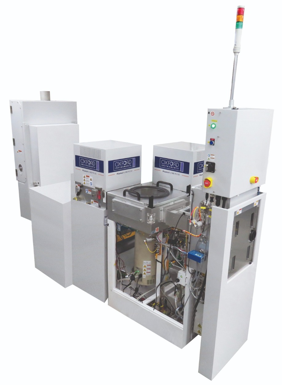
Atomfab is a newly released product that sets a new benchmark for plasma-enhanced, atomic-layer deposition.
“We have already had success with customers, VCSEL manufacturers for example, transitioning from corporate R&D into high-volume manufacturing,” says Gansser-Potts. “We achieve this by truly understanding the customer’s devices and how our systems can enhance the performance of these devices.”
The strategy of Plasma Technology is to focus on critical layers and steps within the device process flow, where it has a deep understanding and can bring value. It can increase device performance, while bringing down the cost of the wafers, says Gansser-Potts. “We have major investment across the company to achieve this.”
Some of the companies that Gansser-Potts and his colleagues are working with are device makers that are in the late research stage, or in the corporate research stage. For these firms, Plasma Technology is accompanying them on their journey to production. When they succeed, Plasma Technology’s tools are qualified before the chipmaker enters high-volume production.
Working with a client in this manner is beneficial on two fronts says Vice-President of Strategic Production Markets, Brian Dlugosch. He points out that it brings in revenue from the outset, and it leads to sales during the manufacturing phase. “That allows you to make money with your equipment for a longer period of time.”
Plasma Technology is also well-positioned to assist in the R&D sector, where the company has held a strong position for decades. Today it is showing no signs of complacency, having recently appointed a market specialist to oversee its activities in that area. Staff are also being recruited to support the production side of the business, where there has been the launch of new software and hardware.
“We have just launched Atomfab, for example, which is much faster than any product we have produced before for atomic layer deposition,” says Gansser-Potts. “And we are just launching PTIQ, which is our control software that is much more tailored to a production environment.”
With so many market opportunities available right now, it is critical to direct efforts at the ones offering the best chances of success. “If we try and spread the net too wide, we will have a small amount of many different markets,” reasons Gansser-Potts, who has adopted and led a well-defined strategy: focusing on really critical processes where Plasma Technology has a competitive advantage and a relationship with the developing client base.
A plasma portfolio
By offering a portfolio of tools, the engineers at Plasma Technology can help customers to find the most suitable one for their needs. For example, if device makers need to etch AlGaN, they can choose between equipment that provides an inductively coupled plasma etch and that producing an atomic layer etch.
In addition, customers may choose to buy several tools, each carrying out a different step in the production process. One obvious benefit is that the fab has to deal with fewer tool suppliers. But that’s not the only gain – it also allows the use of a cluster system, which can improve the quality of the interface between the oxide and the semiconductor, by avoiding vacuum breaks between process steps.
Rewind the clock a few years and many customers would buy tools, shut the door and rarely communicate with their supplier. Today, however, that’s not the norm – many chipmakers now want assistance and support. “We see customers that are in corporate R&D that are willing to pay big service contracts, saying yes we want maintenance, yes we want spare parts,” explains Mark Dineen, Technical Marketing Manager at Plasma Technology.
It’s a change that reflects the gradual shifting of the compound semiconductor industry towards the working practices of the more mature, more open silicon industry. There, market strength is reached by helping customers to increase the number of good wafers produced each day, while lowering the cost. The chipmakers in the silicon industry are not concerned by the appearance of the tool. Klaas Wisniewski, Strategic Business Development Director, hopes that the compound semiconductor industry moves in the same direction, placing value on how Plasma Technology can help to lower cost, increase throughput and enable device functionality.

Oxford Instruments hasdeveloped new processing solutions in its fully equipped lab in Yatton, UK.
Efforts on all these fronts are supported by the work in the Application Lab. In the last decade, the company has made much investment in this, installing 25 process chambers at their main facility, and another seven at a facility in Taiwan. Using these chambers, Plasma Technology’s engineers undertake marathon runs and see if there are any changes to process or material characteristics. This allows the company’s technical team to advise on when it is necessary to clean a tool, and how far a particular parameter can shift before it changes the material properties. Assessments are made with a suite of characterisation techniques that include ellipsometry, atomic force microscopy, scanning electron microscopy and confocal microscopy. A Raman spectrometer is being installed. To obtain device results, Plasma Technology collaborates with companies and universities.
Supporting customers
If firms that have invested in Plasma Technology’s tools run in to problems, engineers can pay a visit and help find a solution. When an emergency occurs, responses are quick wherever the customer may be, thanks to qualified engineers located at seven sites – one is in China, another in Japan, and there are also those in the US, Germany, Singapore, Taiwan and the UK. However, these days, thanks to remote access of data from tools, often all that’s needed is a ‘phone call.
“We have seen a huge growth in remote access to our equipment, so there is less need for hands-on,” explains Dean Furlong, Engineering and Global Services Director. “Two years ago we had pretty much zero remote access. We are now doing thousands and thousands of hours every month of remote support with our customers, whether that is advice, support or improvements.”
This is a significant change, as in years gone by, most chipmakers would have never shared any of their data with equipment manufacturers.
“We are trusted, and trusted significantly, but I don’t think it’s about us,” says Furlong. “It’s about a change in understanding the way the technology works.” A protected environment provides data transmission up to the cloud. For some device manufacturers, a willingness to share data also reflects a narrowing of their view in what is proprietary.
While some customers will welcome a closer relationship with a toolmaker, there are others that prefer to get on by themselves – at least, until there is a problem they can’t fix! For firms with that philosophy, Plasma Technology offers self-sufficiency packages. Once the chipmaker has bought the tool, its engineers are trained and certified on that equipment, so that they can manage themselves and utilise the software. However, if problems arise that they are unable to address, they can access immediate support by phone, and if necessary, have a visit from a Plasma Technology engineer, all as part of the package agreement.
There are an increasing number of products to help customers in the fabs with diagnostics and support assistance. “We have something called LiveAssist, which enables us to have real-time connectivity to site, giving augmented reality support,” says Furlong. Another improvement is the launch of the latest version of the company’s software platform. “Within that there are modules on the roadmap for analytics and diagnostic suites, which will give further enhanced capabilities, not just for ourselves, but for our customers, in terms of understanding what is happening in their environment, and being able to do predictive analytics in tool behaviour.”
“That predictive software is important because people don’t want to operate in a run-to-fail mode,” says Dlugosch. Instead of using a component to the end of its lifetime, engineers are now changing it at an earlier stage so that they can maintain production.

A new software control solution delivers enhanced experience in a production environment.
Deposition developments
At the SemiCon West exhibition last July, Plasma Technology added to its portfolio of atomic scale processing systems with the launch of AtomFab. It provides atomic layer deposition, and is designed to cater for the needs of makers of GaN power and RF devices.
“It really builds on our expertise on controlling the interfaces and ensuring that plasma processing is low damage, but also delivers high-quality and high throughput,” says Aileen O’Mahony, Product Manager, Atomic Scale Etching.
Dineen says that the introduction of AtomFab has gone extremely well, including the process transfer from the R&D platform to the high-volume manufacturing platform. “We maintained process performance at the device level while reducing the manufacturing cost per wafer for this process step by 75 percent.” The company secured its first high-volume manufacturing production order five months after the product launch.
There have also been successful customer demonstrations provided at Plasma Technology’s site, and interest from chipmakers working with other devices that have concerns related to plasma and substrate damage.
During the development of the AtomFab, engineers at Plasma Technology engaged with customers that would consider using this tool for development or production, in order to understand their priorities. “That’s really key, because we need to understand what they are working towards, because that will define the features,” says O’Mahony. The team also wanted to discover what features the customer didn’t value, to avoid including unnecessary capabilities.
While some device manufacturers will be keen to buy a new tool, others will want to upgrade what they already have. That’s possible, as detection systems and new software can be added to existing equipment to enhance its capabilities. However, some tools are now well off the pace – they can date back as far as the early 1980s – and if that’s the case, it’s more prudent to invest in state-of-the-art equipment.
Enhanced etching
For many years, Plasma Technology has offered tools for inductively coupled etching. Very recently, they have been complemented with equipment that can remove material by one atomic layer at a time. Together, these two etching techniques are ideal for the production of normally off AlGaN HEMTs, which have very thin layers, and a two-dimensional electron gas that must not be damaged. Inductively coupled etching can remove most material in good time, before atomic layer etching carefully takes away the last few atomic layers with great accuracy.
As the compound semiconductor industry has evolved, a growing number of device makers are having more stringent requirements related to the geometry of the processed wafer and the yield. This reflects the greater complexity of the design of many of today’s devices.
“If you take a HB LED, you can get away with a lot more, because it’s a larger area,” says Rob Gunn, Senior Product Manager. With a microLED, the sidewalls have a far greater influence over device performance, so there is more concern related to their quality. Having worked with microLED pioneers from their development days, Plasma Technology is well placed to have tools and processes for high-volume production of these devices.
Global goals
Given the capability of Plasma Technology’s tools to process SiC and GaN materials, it’s of no surprise that it is keen to have a strong presence in the Japanese market, where there is the likes of Fujitsu, Sumitomo, Sony and Nichia. But winning sales is far from easy. “The Japanese market is very, very demanding, and it’s culturally probably very challenging for the Western World,” says Wisniewski. So to try and get around these obstacles, Plasma Technology is working with a Japanese process partner, Ulvac. “We have a commercial agreement with them to help us commercialise our technology in the Japanese market.”
China may be best known for its highly competitive LED manufacture that has led to the commoditisation of this device. However, it is also active in other sectors of the compound semiconductor industry, where there are more promising opportunities for Plasma Technology. Right now, the Chinese government is working on the draft of its next five-year plan, which includes the classification of compound semiconductor materials under the third generation of semiconductors. “So it’s big exposure into SiC, where we have qualified processes,” say Wisniewski, who can also see a growth in activity in GaN RF, GaAs optoelectronics and microLEDs – all areas where Plasma Technology has great strength in critical processes.
For makers of these devices in China and beyond, Plasma Technology is a valued partner. For almost forty years it’s been looking after its customers by developing and refining hardware and associated critical processes – fulfilling their wishes is in its DNA.
Engineers at the US Air Force Research Laboratory are propelling the performance of gallium oxide devices to new highs, by realising record-breaking critical field strengths and making the first FETs with switching losses below those for silicon
BY RICHARD STEVENSON
If you have to begin from scratch, it’s very hard to develop a device with a new material. Efforts may have to begin by learning how to grow the crystals that are large enough to be sliced into native substrates. Much research may also be needed to work out how to deposit epilayers, make devices, test them, and then refine the processes. All this requires funding and a team of researchers with the right expertise to define an application space. Given all these challenges, it’s no surprise that progress on making devices with a new material is far from immediate, with some groups only entering the field when they can draw on the success of others.
That’s certainly the case with gallium oxide. Its attractive credentials have been known for many years – it is a material with an incredibly wide bandgap that indicates that it should make devices that are great for power switching – but it is only in the last decade that impressive device results have started to emerge from a few groups.
Laying the foundations for all the recent progress are materials scientists in Japan and Germany that developed processes to grow gallium oxide crystals from the melt and deposit epitaxial layers onto this foundation. The first application for gallium oxide was its use as a transparent conductive oxide substrate for GaN LED applications. But then researchers in Japan also made another important breakthrough – in 2012, a team at NICT, Japan, published experimental results showing a high breakdown voltage in gallium oxide devices made from the β-phase of the material.
One group that has noted NICT’s success and gone on to break records by partnering with some material suppliers is a team from the Air Force Research Laboratory (AFRL) at the Wright-Patterson Air Force Base in Ohio. Viewing gallium oxide as a very promising candidate for fast, low-loss power switching, they have attracted much attention by: setting a new benchmark for the critical field strength of gallium oxide FETs; fabricating the first enhancement-mode gallium oxide MOSFET that delivers a high-voltage operation in the off-state; and producing the first gallium oxide FETs with RF gain and a power switching loss below that for silicon.
In the loop
In the early stages, the team at Ohio were led by AFRL Fellow Gregg Jessen. Initially, he directed his team to explore the new material via ab-initio first principles modelling. Results revealed that the velocity and high critical field strength have disruptive potential in fast power switching and RF power applications. Spurred on by these results, Jessen went to build a US gallium oxide research base and forge international partners, in order to gain access to some of the first device-quality samples.
“Gregg inspired not just our team, but the entire nation,” credits Kelson Chabak, now the team leader at AFRL for device research after Jessen accepted a position in industry.
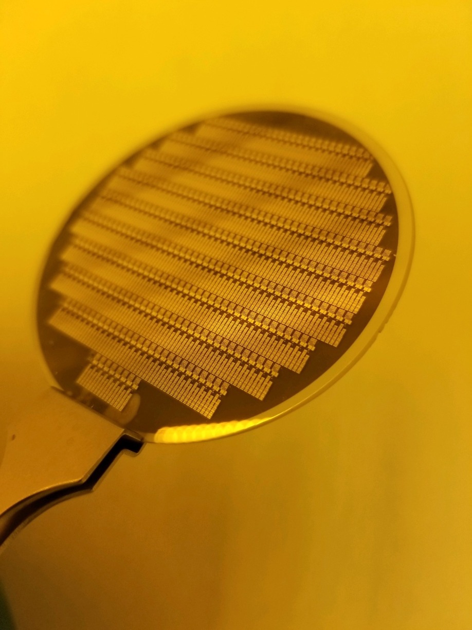
2-inch Synoptics gallium oxide substrate with an gallium oxide epitaxial layer and transistor fabrication completed by AFRL engineers.
Despite his curiosity, Chabak did not intend to change direction and switch from working on GaN to gallium oxide: “We weren’t too invested in [gallium oxide] at the time. In fact, we were ready to pass on it if our early assessment of devices were to fail.”
To evaluate the potential of this ultra-wide bandgap material, Chabak and his colleagues leaned on their international partners for epistructures. Although they had access to MBE tools at AFRL, they were primarily configured for fundamental research in GaN (Chabak and colleagues have tremendous expertise in this area, following two decades of work providing rapid feedback to the GaN material community).
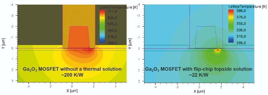
Technology computer-aided design simulation of thermal effects without and with a top-side solution implementing flip-chip technology, thickmetal contacts, a thermally conductive passivation dielectric on the channel and aggressive lateral scaling in a gallium oxide device.
Sourcing material
Substrates came from Tamura, the only commercial supplier. This firm, which has worked closely with NICT, uses the edge-defined, film-fed growth process to produce material that is up to 4-inch in diameter in some orientations. Substrate dimensions for one of the most common orientations were initially 10 mm by 15 mm, but in the last year Tamura has also started to offer variants that are 25 mm by 25 mm. There is no observed degradation in quality with the larger sizes, according to Chabak, while price per unit area has fallen by around 50 percent.
The team at AFRL purchased these substrates and contacted Tamura’s spin-off, Novel Crystal, to purchase epiwafers. In addition, the AFRL relied on another source of epitaxial growth, the Leibniz Institute for Crystal Growth, a facility more commonly known by the initials IKZ.
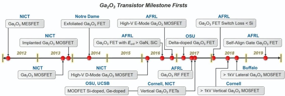
The researchers at AFRL have provided several significant contributions to the advance of gallium oxide devices.
By shipping high-quality material in good time, IKZ played a critical role in AFRL’s success. “We were able to become leaders in our field because we secured early access to materials,” admits Chabak.
The first milestone for this collaboration came in 2016, when AFRL device team member Andy Green fabricated and reported a MOSFET made from an IKZ epiwafer that blocked 230 V over a 0.6 μm gate-drain drift region. That translates to a record-breaking average critical field strength of 3.8 MV/cm. To put this figure in perspective, most lateral GaN devices, after a few decades of research, operate at 1 MV/cm. “So without much optimisation, we got about four times the critical field strength of GaN,” enthuses Chabak. “That was the spark that started the fire.”
Green’s record-breaking result came from an epiwafer made by MOCVD at IKZ, with growth on an off-cut substrate to optimise the diffusion length of the adatoms. Note, however, that Chabak and his colleagues have also obtained good results on MBE-grown material, provided by Novel Crystal, so they are yet to decide on what growth technique is better for gallium oxide homoepitaxy. “The jury is still out, we’ve made good devices on both, and we are still assessing materials.”
Side-stepping p-type problems
Later that year, the team from AFRL reported the first ever enhancement-mode FET with a high-voltage operation in the off-state. This ground-breaking result is important, as it shows that it is possible to fabricate a normally-off FET, despite the lack of p-type carriers in gallium oxide. Normally-off operation is highly valued, as it creates a device that is fail-safe, and can be driven with a unipolar power supply.
The key to this success is to employ the work function of the gate to pinch-off an array of non-planar fin channels. “We were the first ones to implement this with gallium oxide, but very similar things have been done with GaN,” says Chabak.
Note that it would have been folly for Chabak and his co-workers to try and attack problems associated with p-type doping in gallium oxide head on. Holes are self-trapped, so they fail to contribute to carrier transport, and the flatness in the valence band results in a very heavy hole mass.
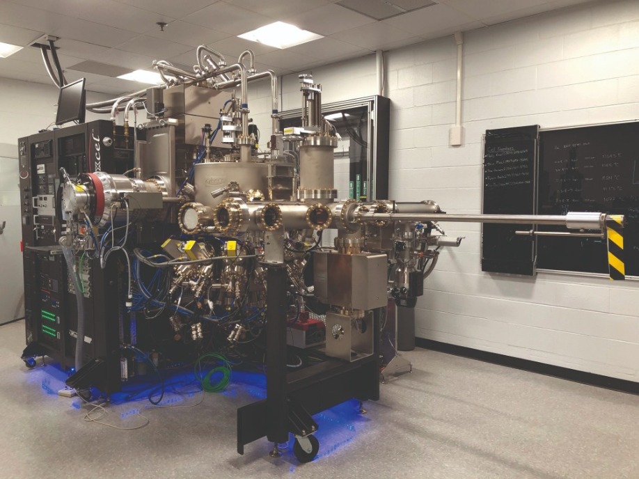
Veeco GenXcel oxide MBE tool located at AFRL dedicated to fundamental oxide materials and device research on up to 4-inch substrate sizes.
Implantation is another option for producing n-type material. Chabak views this as a tool that offers device engineering and lateral doping profiles, and allows the fabrication of transistors with self-aligned contacts – features that are difficult to implement in GaN.
Compared to wide bandgap materials, the temperature required to activate carriers in gallium oxide is quite low – in some circumstances, just 850 °C will suffice. Studies of this doping technique have led to some interesting results, such as finding that impurities diffuse along implanted, damaged regions.
Better than silicon
Chabak’s team claimed their third record-breaking result in 2018, when they reported the first gallium oxide FET with a switching loss below that for silicon. “There were a few different design tricks that were implemented,” reveals Chabak. Modifications included partially removing the channel to make it normally off, adding a gate-connected field plate to reduce the peak electric field and optimising device dimensions. Resistance fell by reducing the source-to-drain distance, a feat realised without sacrificing the breakdown voltage.
Efforts at AFRL have also included an investigation of the RF characteristics of gallium oxide transistors. “We are very careful to say that we do not see gallium oxide replacing gallium nitride for RF devices,” warns Chabak. “Gallium nitride devices will always be the king of RF power.” However, he thinks that gallium oxide could become a complementary technology, as transistors made from this material may have the potential to provide a high efficiency, or deliver a higher output power, when configured in a particular class of operation.
The team has investigated the RF characteristics of devices with a 0.7 μm gate length and a gate-recess, which reduces the channel thickness from 180 nm to around half that value. Small-signal measurements, using a drain-source voltage of 40 V, revealed a cut-off frequency and maximum oscillation frequency of 3 GHz and 13 GHz, respectively. Driven in class A mode, output power is 0.23 W mm-1 and the power added efficiency is 6.3 percent, according to CW large-signal power measurements at 800 MHz.
Severe heating limited the performance of these RF devices. That’s also the case for most power devices made from gallium oxide, as both types of device are impaired by the low thermal conductivity of this material. Some critics claim that this is a severe impediment for the progress of this class of device, but Chabak disagrees, arguing that it is not a “showstopper”. When discussing this issue with the naysayers, he is quick to point out that the thermal conductivity of GaAs, which is a mainstream RF power technology, is within an order of magnitude of that of gallium oxide.
To ensure that gallium oxide devices fulfil their potential, efforts will have to be directed at extracting heat from both the backside of the device, and the top, where the biggest gains can be made. “We have some preliminary modelling that suggests flip-chip technology can, when combined with backside wafer-thinning, reduce the overall thermal resistance of our devices to close to SiC.”
Realising such success will not be easy, admits Chabak. “I don't expect it to be something that is solved in the near term.” In fact, if significant progress is to be made, it will probably require the funding of major programmes. However, the approaches to explore this can draw on previous successes in the compound semiconductor industry. “Luckily we already have a lot of thermal management solutions, developed for gallium nitride and gallium arsenide. So we hope to take advantage of these.”
Chabak and his co-workers are not planning to tackle this problem just yet. Instead, they will direct their short-term efforts at introducing electron-beam lithography to the fabrication process, and scaling transistors to below a micron. The devices that result could be very attractive candidates for fast-switching applications, by combining very high speeds with high breakdown voltages.
The team mainly collaborates with their gallium oxide materials partners for epiwafers. But that should soon change, as last year the group invested in a state-of-the-art oxide MBE tool that can handle 4-inch substrates and produce gallium oxide epiwafers featuring either silicon or germanium doping. This reactor will also be used to produce heterostructures such as those containing aluminium gallium oxide.
Home-grown support
The introduction of the tool has expanded the number of researchers at the AFRL that are devoting at least some of their time to gallium oxide. A few years ago, efforts involved a smaller group of device engineers, all in the sensors group – but with the MBE machine on site and an exponential boom in interest, they now have participants from materials, devices and power groups across AFRL. “When we have meetings for gallium oxide, we can easily fill a large room now,” says Chabak.
Once epiwafer production is in-house, the team will only need to source substrates. In the near-term they will continue to come from Tamura, but further ahead, they could be obtained from a domestic source. That’s because AFRL has been funding a gallium oxide crystal growth programme at Synoptics, a subsidiary of Northrop Grumman.
“They are well ahead of the curve, because they have made crystals for lasers for a long time,” says Chabak. Using the Czochralski technique, Synoptics has been able to grow, fabricate and polish semi-insulating (010) substrates up to 2-inches in diameter.
In the last few months, the team at AFRL have started to make devices using these substrates. “Are they comparable to Tamura? Some are – we’re getting there,” says Chabak.
In addition to this funding, AFRL recently initiated a program with Saint Gobain for edge-fed film growth of semi-insulating, (010) 2-inch gallium oxide substrates.
Creating domestic sources for large area gallium oxide substrates will be the missing piece for Chabak and his device team. In turn, this should lead to enhanced research and development, giving the team from the AFRL a good chance to add to their tally of record-breaking results for gallium oxide devices.
Switching to a silicon foundation and re-using germanium substrates offer two options for driving down the cost of multi-junction cells
BY RICHARD STEVENSON
THROUGH NO FAULT of its own, CPV may appear to have missed the boat. Many leading firms developing this technology have been killed off by a double whammy – a credit crunch that chocked further investment, and plummeting prices for silicon PV that blunted the competitive edge of this class of photovoltaics.
Given this state of affairs, it’s hard to see how CPV will ever make an impact. Today silicon dominates, and it is sure to do so for many years. But look further down the road and a more promising picture emerges. Any further gains in silicon cell efficiency are going to be marginal, limiting the performance of this technology, and production is already streamlined, so manufacturing costs are only going to show modest declines. This implies that electrical generation costs associated with silicon are only going to fall fractionally in the coming decades. Due to this, there is a good chance that CPV can catch up. And given its far higher efficiency than all forms of silicon single-junction cell, it promises to be particularly competitive in situations where the cost of land is at a premium, and there is a strong desire to generate as much power as possible from a plot.
To get CPV to a position where it has a chance of market success, efforts must be directed at investigating all the possibilities for increasing its competitiveness. Making cells more efficient, possibly through the use of more junctions, will improve the solar yield. Another lever is to reduce the cost of the tracker, along with making it lighter, as this trims shipping costs. And increasing the level of concentration is another promising option, as it allows fewer cells to generate a given output power.
Within this mix, there is also the opportunity to reduce the cost of the substrate. About one-tenth of the cost of the entire system is tied up in the cell, with the lion’s share attributed to its foundation. According to a study by the US National Renewable Energy Laboratory (NREL), in a GaAs solar cell the substrate accounts for 84 percent of the cost the device.
One group developing ways to cut the cost of the substrate is that led by Abderraouf Boucherif from the University of Sherbrooke in Quebec, Canada. His team, whose work is attracting much interest from industry, has not just developed one approach to slashing substrate costs – it has pioneered three distinct technologies. They are: introducing porosity to a germanium-on-silicon template, so that it can become a platform for making high-quality triple-junction cells; etching an epitaxial structure from its germanium substrate so that the latter can be re-used; and combining graphene and porous silicon to create a flexible, light-weight foundation for high-efficiency photovoltaics.
Porous silicon
The benefits of using a silicon substrate are not limited to a reduction in cost, but extend to a higher thermal conductivity, leading to a reduction in thermal management. According to Boucherif, in turn this diminishes the chance that a cell will ‘burn’, and increases its efficiency, thanks to a lower operating temperature. “These are not necessarily huge impacts, but it could give a little boost to the cell.”
Silicon is also stronger than germanium. This increases the robustness of the cell, and reduces the likelihood that a wafer will break during the fabrication process.
A third advantage of silicon over germanium is the larger diameter of the substrates, enabling an increase in manufacturing efficiency. This could be realised by processing in silicon fabs. A study by a team at the University of Ottawa has found that costs could reduce by up to 70 percent by switching the substrate from 100 mm germanium to 200 mm silicon.
The big concern with using silicon as the substrate for making triple-junction cells is the dislocation density in the epilayers. Dislocations degrade device performance by trapping the photogenerated carriers, dragging down efficiency.

Figure 1. When a germanium film is grown on silicon, the difference in lattice constants leads to the generation of many dislocations. These imperfections can be addressed with a process that begins with electrochemical porosification, which creates voids in the material. Annealing follows, with elevated temperatures promoting the coming together of two dislocations with opposite Burgess vectors that are attracted to the void. They glide together before annihilating, at which point they disappear from the surface and are trapped by the void. Dislocation-free material results, proving a platform for the growth of III-V cells.
His team are able to produce germanium films on silicon substrates with a dislocation density well below this limit by using an electrochemical porosification process. According to Boucherif, this is a very simple, industry friendly self-organised process with very low costs. “No lithography or preparation steps are needed.”
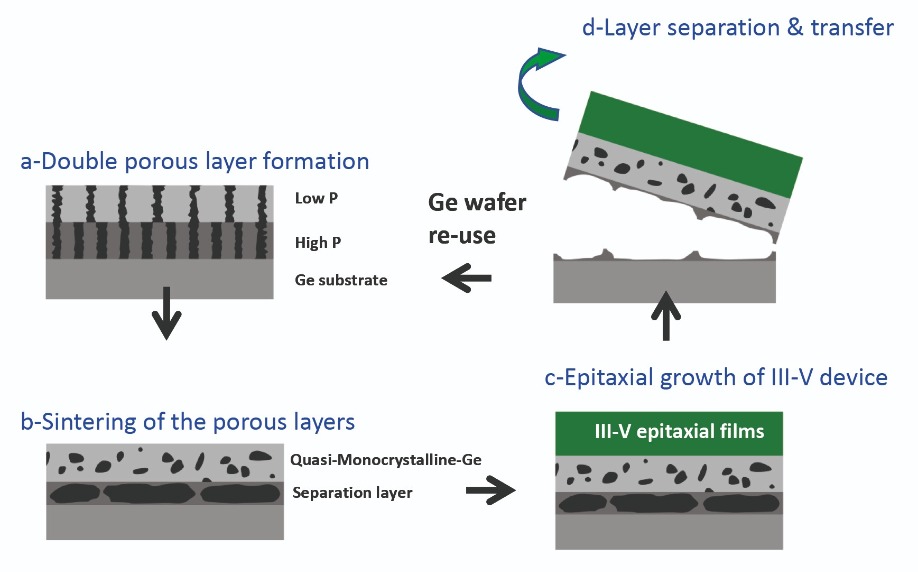
Figure 2. Re-use of germanium substrates begins with a formation of a high-porous and a low-porous layer (a). Sintering results in a quasi-crystalline germanium layer near the surface (b) that provides a platform for III-V growth (c). Electrochemical etching removes the separation layer and allows the substrate to be removed and reused.
Boucherif and his co-workers have broken new ground by applying the process to germanium, rather than silicon. After growing a film of germanium-on-silicon, an electrochemical porosification process produces nano-scale voids in the epilayer (see Figure 1). Annealing at elevated temperatures for several minutes changes the profile of the pores in a process that irradiates dislocations, to yield a high-quality surface for subsequent III-V growth.
To demonstrate the power of this technique, the team have applied it to part of a 100 mm wafer, and compared the dislocation density to that of an untreated region. Using the electrochemical porosification process, the dislocation density plummets from around 107 cm-2 to just 104 cm-2.
Processed material is evaluated by scanning electron microscopy, transmission electron microscopy and X-ray diffraction. These techniques reveal that the team’s technology creates material that forms a barrier to dislocation propagation.
Germanium re-use
An alternative option for cutting cell costs is to continue to use germanium substrates for the growth of III-V cells, but after this, separate the active region from the substrate, which can be re-used.
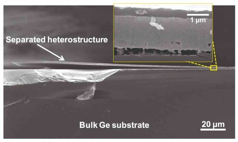
Figure 3. Separating the heterostructure from bulk material enables the re-use of germanium substrates.
Their approach begins by forming two regions within the germanium substrate: and upper layer, with a low porous density; on top of another layer with a higher porous density. Annealing transforms this into an upper quasi-monocrystalline layer sitting above a separation layer (see Figures 2). This step can be carried out by loading the material into an epi-reactor, and carrying out annealing prior to the growth of the III-V film. Separation follows, based on etching with a mixture of hydrofluoric acid and ethanol. For this, the team uses a two-step process, so that passivation can be applied after etching to prevent the dissolution of the removed germanium (see Figure 3).
Success with this approach has been proven by Boucherif and co-workers. They have grown a 400 nm-thick GaAs film on quasi-monocrystalline germanium. The GaAs is monocrystalline, according to X-ray diffraction.
Mesoporous silicon
The third solution proposed by the team is based on the use of mesoporous silicon, which is an incredibly flexible free-standing membrane. Its production involves porosification, followed by electro-polishing that creates free-standing material.

Unfortunately, mesoporous silicon is unsuitable for epitaxy, because it is unstable at the required growth temperatures. But Boucherif’s team has found that adding graphene addresses this weakness and allows epitaxy.
That is not the only change, however – it also introduces some strain. “That is one of the ways of adjusting the lattice parameters,” says Boucherif, who adds that the composite can also be used as a compliant substrate, because it is flexible and stable during epitaxial growth.
Very recently the team have used these mesoporous silicon and graphene structures as the foundation for the growth of GaN films. That might seem an odd choice, since GaN is not used in multi-junction cells. However, there is a good reason for growing this material – as it requires a very high growth temperature, if success results, it should be possible to apply this technology to all III-V film growth.
Comparing the quality of this GaN to that grown on bulk silicon reveals an improvement. “We see a reduction in crack density,” says Boucherif, who is quick to point out that more work must be done before high-quality GaN epilayers are produced.
From materials to devices
Additional plans for the future include a shift from characterising materials to evaluating devices. For that objective, Boucherif and his team could not be better placed – the university has a solar park on its campus that has been up and running for a year, and provides a test site for various photovoltaic and thermal solar technologies.
As well as generating up to 1 MW of power – that equates to about 15 percent of the university’s electricity needs – the site is helping to evaluate the reliability and performance of solar cell technologies under a variety of weather conditions. “In Quebec, we have in summer more than 30 degrees, and in winter down to minus 25,” says Boucherif.
Devices made by his team can be placed in one of eight CPV systems, each with a peak output of 30 kW, based on a technology that originated at Concentrix. All the systems have been deployed by Saint-Augustin Canada Electric Inc (STACE), which manufactures the CPV systems in Trois-rivieres in Quebec, Canada, using carbon-free hydro-electricity.
The solar park is clearly going to play a role on the future development of terrestrial triple-junction technology. This facility will hopefully demonstrate that it is possible to make reliable, highly efficient multi-junction cells that are free from high substrate costs, and ultimately help to rekindle the prospects for CPV technology.
Y. Bioud et al. Nat. Commun. 10 4322 (2019)
A. Boucherif et al. Appl. Phys. Lett. 102 011915 (2013)
J. Ward et al. Prog. Photovolt: Res. Appl. 24 1284 (2016)
Next-generation mobile devices, data infrastructure and communication networks could be aided by three-dimensional, monolithic integration of GaN and silicon CMOS on 300 mm wafers
BY HAN WUI THEN FROM INTEL CORPORATION
THE TRANSITION to 5G and beyond is tipped to drive an exponential increase in the number of connected mobile devices. The integrated circuits that power them will need to provide greater energy efficiency, in a smaller form factor. Consequetly, there is much demand for more capable transistors and the integration of ever-larger numbers of components on the microchip.
Fulfilling these requirements is far from easy, as none of today’s transistor technologies are capable of meeting the diverse needs associated with power delivery and RF front-end design. Due to this issue, circuit designers are combining many distinct, separate chips. This is not great, as it results in a bulky package.
To tackle this problem, our team at Intel’s Components Research division in the Technology Development Group of Oregon has developed the first monolithic, three-dimensional GaN and silicon transistor stacking technology. It delivers best-in-class performance and efficiency, while allowing diverse functionalities to be integrated on a single chip.
Combining silicon and GaN is an attractive proposition. Silicon is today’s workhorse for power electronics and RF switches, but it struggles to deliver high-frequency, high-power performance, so it is not a good choice for RF power amplification (see Figure 1). For that particular task, GaAs HBTs, GaAs HEMTs and GaN HEMTs are the front runners. However, these technologies are not ideal for making efficient power electronics: depletion mode GaAs HEMTs and GaN HEMTs are not favoured, due to their always-on nature; and the GaAs HBT is unsuitable, being current-driven rather than field-driven.
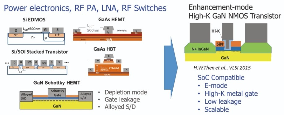
Figure 1. In today’s power delivery and RF front-end solutions, dissimilar technologies come in multiple distinct and separate chips that have to be made to work together in a bulky package. Enhancement mode GaN transistors enabled by high-κ dielectric and metal gate technology can enable, for the first time, all these functionalities to be integrated on a single chip, realising a system-on-chip (SoC).
One of the successes that has come from our efforts is the fabrication of the first high-performance GaN transistors on 300 mm silicon (111) wafers (see Figure 2). We make these transistors with a 300 mm process technology that is compatible with leading CMOS fabs.
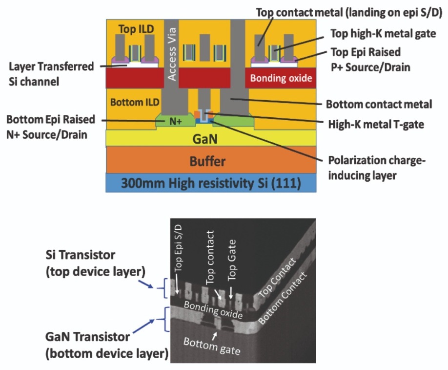
Figure 2. Intel has produced the first GaN transistors on a 300 mm silicon (111) wafer in one of its leading CMOS fabs. Its researchers have employed a new technique of three-dimensional monolithic integration by layer transfer to stack silicon PMOS transistors on top of GaN NMOS transistors to enable CMOS functionalities, for the first time in industry.
Using one of our leading CMOS fabs for processing our GaN transistors on 300 mm silicon reaps an additional reward – it opens the door to all the latest process innovations. They include high-κ technology, three-dimensional layer transfer, chemical-mechanical polishing, lithographic techniques and copper interconnects. In addition, we benefit from the significant reduction in cost associated with cheaper 300 mm silicon substrates and high-volume production.
Leveraging larger wafers
Due to the lack of native substrates, nearly all GaN is grown on foreign substrates, such as sapphire, SiC and silicon. The most popular platforms are 3-inch and 4-inch SiC, which are both relatively expensive, and 4-inch, 6-inch and 8-inch silicon (111). In contrast, we are using cost-effective 300 mm silicon (111) substrates (see Figure 3). On this platform we marry GaN with the most advanced high-κ dielectric metal gate technology in our 300 mm fab. This enables enhancement-mode operation and gate-stack scaling, and it ultimately realises high performance and low leakage, the keys to higher efficiencies. Note that this reduction in leakage is significant – it can exceed four orders of magnitude (see Figure 4) better than a Schottky gate GaN HEMT.
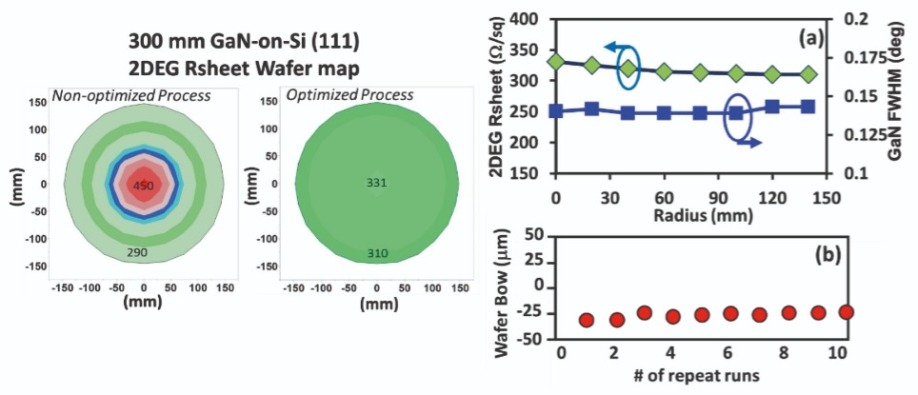
Figure 3. Optimised and uniform data from a manufacturable 300 mm GaN epitaxy process at Intel. Data distributions shown include: two-dimensional electron gas sheet resistance; GaN crystal quality, evaluated in terms of the the x-ray diffraction peak’s full width at half-maximum (FWHM); and 300 mm wafer bow.
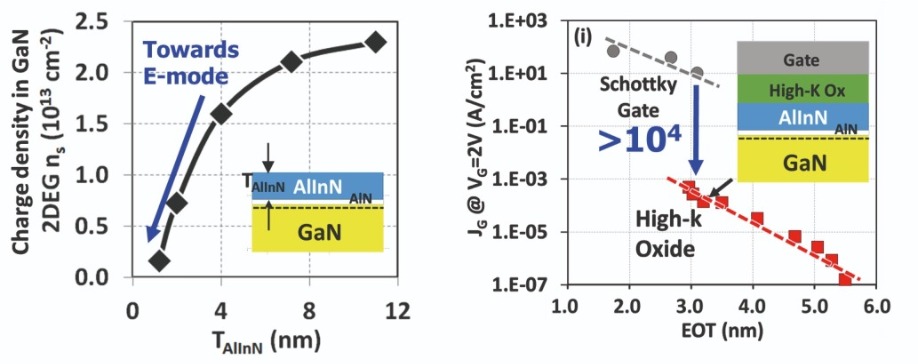
Figure 4. A high-κ gate dielectric reduces gate leakage by more than four orders of magnitude at scaled equivalent oxide thickness (EOT) for higher performance.

Figure 5. The ID-VD characteristics of Intel’s e-mode high-κ dielectric GaN NMOS transistor on a 300 mm silicon wafer showing a high drive drain current that is approaching 1.5 mA/mm, a low knee voltage (it is below 1 V), and an on-resistance, RON, of just 610 W-Ωm. Low drain leakage, with IOFF as low as 100 pA/mm at 5 V drain voltage, and excellent RON can be achieved simultaneously. The high-κ e-mode GaN NMOS transistors are about four times better than silicon transistors used for power delivery.
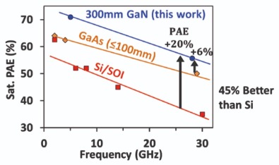
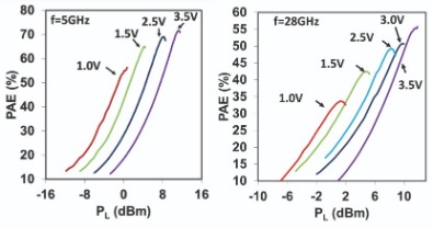
This value is well below the minimum cut-off supply voltage for a typical GaAs HBT, highlighting the potential of the high-κ GaN NMOS transistor to significantly extend battery life while providing unrivalled efficiencies using the envelope-tracking RF PA architecture. High-κ GaN NMOS transistors also make excellent RF switches and low-noise amplifiers. For example, they have an excellent figure-of-merit for the switch, with a product of on-resistance and off-capacitance of just 110 fs. The minimum noise figure is only 0.4 dB at 5 GHz and 1.36 dB at 28 GHz (see Figure 8).
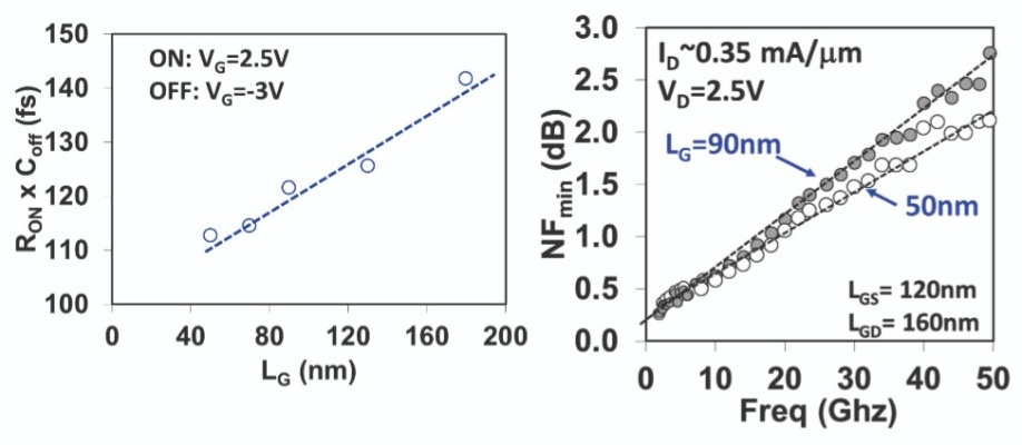
Figure 8. The excellent switch figure-of-merit, RON x COFF, and noise performance, NFmin, of the high-κ e-mode GaN NMOS.
Three-dimensional integration
A selling point in today’s marketplace is tight on-chip integration of CMOS analog and digital logic/control functionalities, along with CMOS memory. These types of CMOS chips are currently built as standalone units, but as functionality and complexity increases, monolithic system-on-chip solutions will be needed to provide higher efficiency, lower cost and a higher integration density (see Figure 9).
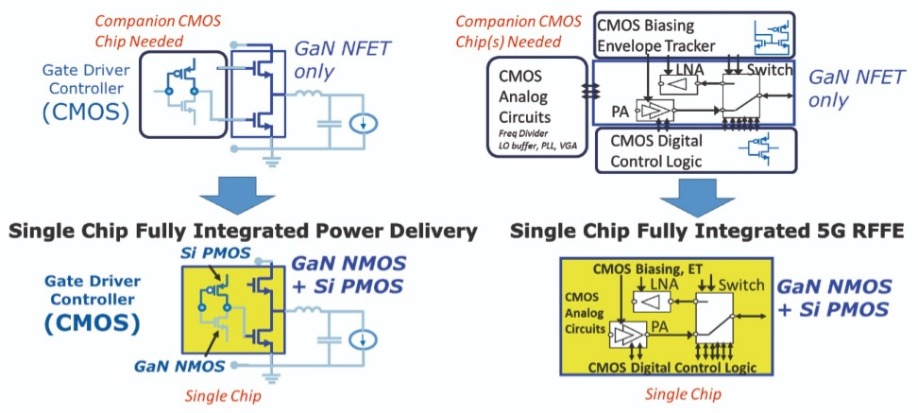
Figure 9. Single-chip fully integrated power delivery and RF front-end units can be realised with Intel’s three-dimensional monolithically integrated silicon PMOS stacked on GaN NMOS transistor technology.
To monolithically integrate multiple dissimilar semiconductor materials on a single silicon substrate, we have turned to layer transfer techniques. This enables us to monolithically stack silicon PMOS transistors on top of GaN NMOS transistors. Drawing on this form of three-dimensional monolithic integration has much merit, as it allows each constituent transistor technology to be built and optimised separately to offer the best performance and cost.
We begin our three-dimensional layer transfer process by oxide fusion-bonding a standard 300 mm crystalline silicon (100) donor wafer to a completed 300 mm GaN-on-silicon (111) wafer. After this, we remove the bulk donor wafer and fabricate silicon PMOS transistors (see Figure 10). We ensure high-performance silicon PMOS by aligning the finfet in an orientation that boosts hole mobility. This is accomplished by having the transistor channel on the sidewalls orientated in a particular crystal plane and current-carrying direction (see Figure 11). There is much freedom with our approach. The silicon PMOS transistor design and architecture can be made independently of the choices for the bottom GaN transistors. For example, by selecting the appropriate channel orientation for the silicon PMOS and the channel length for the GaN NMOS, the drive current and the off-state leakage can be matched for both channels (see Figure 12).
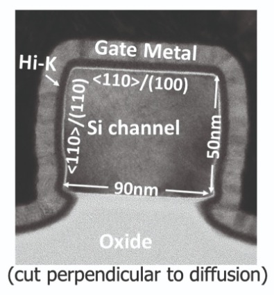

Our monolithic three-dimensional stacking of GaN NMOS and silicon PMOS transistors provides a powerful way to integrate two dissimilar best-in-class semiconductor technologies on the same wafer and deliver the best performance, increased density, and greater functionality.
This technology has tremendous promise as it could enable entirely new classes of products with game-changing capabilities. Many exciting opportunities lie ahead, including the full integration of efficient, high-performance RF and power delivery with standard silicon-based processors. Such a technology has the potential to meet the demands of next-generation mobile devices, data infrastructure and communication networks for 5G and beyond.
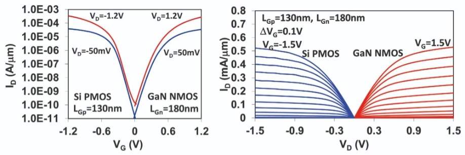
Figure 12. Current-voltage characteristics of the top layer channel length (LG is 130 nm) silicon PMOS transistor and the bottom channel length (LG 180 nm) GaN NMOS transistors. Dimensions have been chosen independently, to match drive current strengths and off-state leakages.
Thanks to its wide bandgap, GaN has vastly superior Johnson and Baliga figure-of-merits when compared with GaAs and silicon (see Table 1). These virtues enable GaN to operate at high frequencies and high power.

Table 1. Intrinsic semiconductor properties and figure-of-merits (FOM) for silicon, GaAs and GaN. N-channel GaN has the highest Baliga and Johnson FOMs, but P-channel GaN remains challenging due to low active p-doping and low hole mobility. The silicon PMOS transistor has a proven complementary P-channel with high hole mobility and high active p-doping.
The resulting GaN heterostructure has a high carrier concentration, and also a high electron mobility, due to the low effective mass of the electrons and the absence of impurity scattering.
Yet another strength of GaN is that, due to its wide bandgap, it has a critical breakdown field that is at least ten times that for GaAs and silicon. This allows GaN transistors to be scaled to smaller lengths, leading to a higher performance. For example, for a supply voltage of 3.7 V, which is that provided by a lithium-ion battery, GaN transistors can be shorter, have a lower resistance and provide a higher drive current. Strengths such as these have made GaN the best semiconductor technology in production today for power and RF performance.
H. W. Then et al. “3D heterogeneous integration of high performance high-κ metal gate GaN NMOS and Si PMOS transistors on 300mm high-resistivity Si substrate for energy-efficient and compact power delivery, RF (5G and beyond) and SoC applications”, IEDM, 2019.
H. W. Then et al. ““High-Performance Low-Leakage Enhancement-Mode High-κ Dielectric GaN MOS-HEMTs for Energy-Efficient, Compact Voltage Regulators and RF Power Amplifiers for Low-Power Mobile SoCs”, VLSI Technology Symposium, 2015.
S. Bader et al. “GaN/AlN Schottky-gate p-channel HFETs with InGaN contacts and 100mA/mm on-current”, IEDM, 2019.
N. Chowdhury et al. “First Demonstration of a Self-Aligned GaN p-FET”, IEDM, 2019.
The demonstration of half-bridges and single-stage buck converters takes GaN power ICs another step forward
BY XIANGDONG LI AND STEFAAN DECOUTERE FROM IMEC
OVER THE LAST FEW YEARS discrete GaN HEMTs have been taking an increasing share of the power electronics market. Thanks to their fundamental superiorities over their silicon rivals. Merits of these wide bandgap transistors include a lower on-resistance, smaller parasitic capacitance and a higher critical electrical field. In addition, GaN HEMTs switch at higher frequencies, enabling power systems based on this technology to be smaller and lighter, due to a reduction in the size of passive components. Yet another attribute of these devices is their reverse conduction capability, accomplished without the need for the low-performance body diode, which is detrimental when deployed in a typical silicon VDMOS power device.
For fail-safe operation, enhancement-mode (E-mode) p-GaN gate HEMTs have been widely accepted by various vendors, and used for a wide variety of applications that range from AC-DC converters and DC-DC converters to bridgeless totem pole power-factor correction circuits and class D Audio amplifiers.
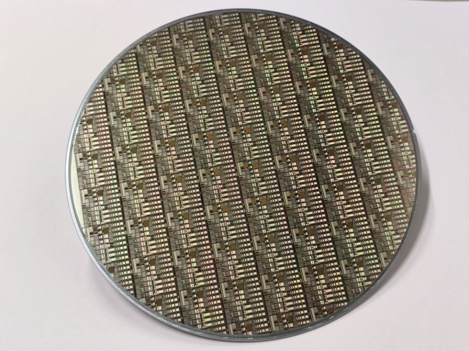
Figure 1. Processed GaN ICs on a 200 mm GaN-on-SOI substrate.
Much effort has been devoted to integrating these single or multiple modules on GaN-on-silicon. Progress is not easy. One major obstacle is that all-GaN ICs on traditional silicon substrates are hampered by a lack of effective isolation – this induces a back-gating effect in the half-bridge. A second stumbling block is the absence of a complementary GaN pFET, which is a bottleneck for integrating high-performance logic circuits and inverting amplifier stages.

Figure 2. GaN IC components on a GaN-on-SOI substrate.
We have already demonstrated the feasibility of our technology for developing functional GaN HEMTs and related components that are key to an integrated all-GaN power IC. This breakthrough has involved activity in many areas, from epitaxy to integration, modelling and simulation. The result is a technology that has proved its worth by the functionality of our GaN power ICs.
Epitaxy and integration
Our team has developed GaN power IC integration technology on 200 mm GaN-on-SOI wafers with very little warp and a high degree of uniformity (see Figure 1). We begin with a 1070 μm-thick silicon (111) handling wafer that contains a 1.5 μm-thick SiO2 buried layer and a 1.5 μm-thick silicon (111) top layer. We load this engineered wafer into an MOCVD reactor and add a 200 nm-thick AlN nucleation layer, followed by a 3.25 μm (Al)GaN buffer layer, a 400 nm GaN channel layer, a 12.5 nm Al0.23Ga0.77N barrier layer and an 80 nm magnesium-doped p-GaN layer with a doping concentration of about 3×1019 cm-3. The stepped superlattice buffer, specifically designed by our team, controls the stress during epitaxy. Thanks to this, we avoid excessive wafer warp.

Figure 3. Cross-sectional transmission electron microscopy images of the (a) 200 V p-GaN gate HEMT, buffer stack, and substrate, and (b) detailed gate module, and focused ion beam, scanning electron microscopy images of the (c) 6 μm-wide trench isolation and (d) substrate contact.
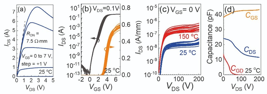
Figure 4. (a) Output, (b) transfer, (c) off-state leakage, and (d) C-V characteristics of the fabricated 40 mm p-GaN gate power HEMT on the 200 mm GaN-on-SOI substrate. The device shows a low Ron of just 7.5 Ω mm, a uniform high Vth of more than 3 V, and an off-state leakage of less than 1 µA/mm.
Evaluating modules
One significant weakness of conventional GaN-on-silicon HEMTs is that their low side and high side share the same common conductive silicon (111) substrate, which is normally grounded. Due to this, when the high side is switched on, the drain current is jeopardized dramatically by the negative substrate-to-channel potential difference. In contrast, with our approach, this potential difference is fixed at zero, thanks to the local substrate contact and deep trench isolation. This architecture guarantees a very stable high-side drain current, and ultimately eliminates the back-gating effect, paving the way to GaN power ICs.
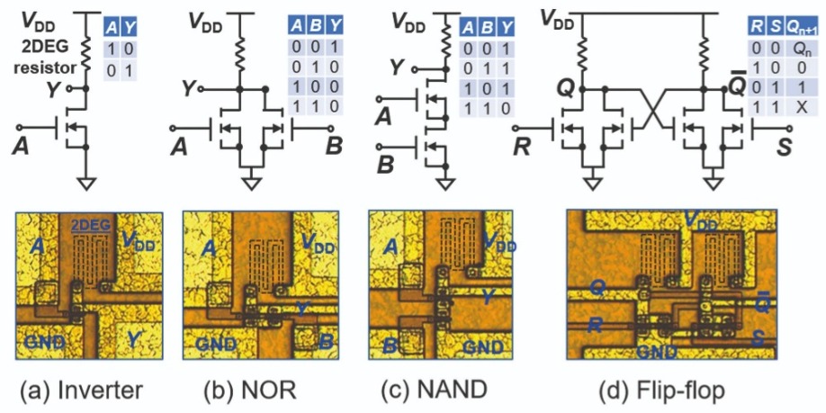
Figure 5. Schematic, truth table, and photograph of (a) inverter, (b) NOR gate, (c) NAND gate, and (d) flip-flop, designed in resistor-transistor logic.
After packaging these fabricated blocks, we evaluated them with switching tests. The results are encouraging, with waveforms that exactly follow the truth tables (see Figure 6). Thanks to this success, we have been able to construct more complex ICs in power systems, such as diagnostic and protection circuits, based on these fundamental blocks.

Figure 6. Measured switching waveforms of the (a) inverter, (b) NOR gate, (c) NAND gate and (d) flip-flop.

Figure 7. (a) The double pulse test (DPT) circuit, (b) packaging of the GaN IC with an integrated driver and power HEMT, (c) printed circuit board (PCB), and (d) DPT switching waveforms and current handling capability of the HEMT with integrated driver.

Figure 8. (a) imec’s GaN IC with integrated half-bridge and drivers for use in a buck converter, (b) photograph of the fabricated half-bridge with integrated drivers, (c) test board, and (d) test setup.
For the GaN IC design, we modified MIT virtual source GaN HEMT models for E-mode p-GaN gate HEMTs and used spice models for the resistors. We have designed a monolithically integrated all-GaN buck converter using our 200 V GaN IC platform process design kit, which includes process documentation, library devices, layout guidelines for custom design, verification and models (see Figure 11).
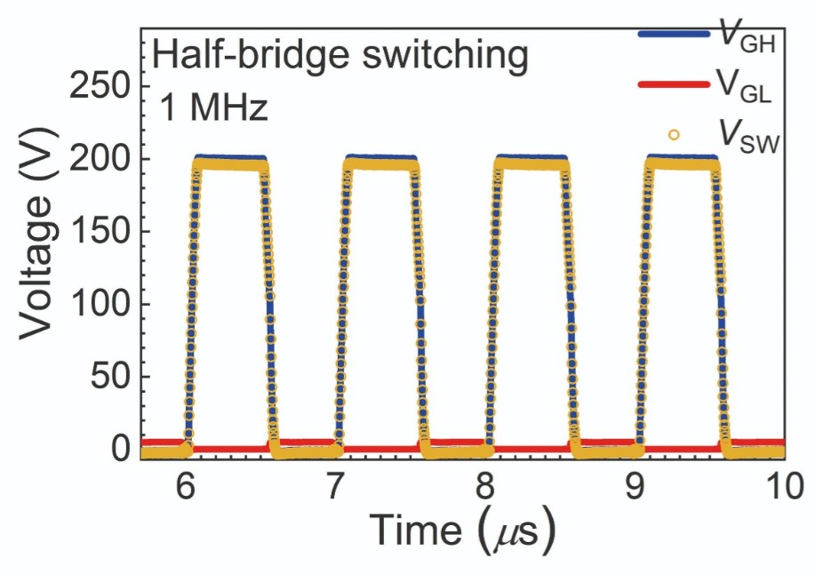
Figure 9. The 200 V half-bridge switching test is first executed on the test board by disconnecting the output stage of L, CO, and Rload. Two 1 MHz non-overlapping signals, HI and LI, with a dead time of 40 ns, are sent to the two driver input terminals and the waveforms of VGH, VGL, and VSW are monitored. Previous studies show distortion of switching waveforms, due to the back-gating effect in a half-bridge on GaN-on-silicon without substrate isolation. In this case, the back-gating effect is fully mitigated thanks to the trench isolation.
This GaN IC is a major milestone in the advancement of this technology, as it is the first step towards a real smart power IC based on p-GaN technology. Note that the designed all-GaN ICs have been successfully processed on 200 mm GaN-on-SOI (see Figure 11(c)).
Given that this work is still in its infancy, it is not surprising that there is still room to improve the performance of our GaN ICs. We have noticed that the resistor-transistor logic is impaired by high static power dissipation and a long RC delay, which are problematic for some high-speed analogue ICs. But the good news is that we are developing new integration technology. This includes integrating a depletion-mode HEMT, which replaces the two-dimensional electron gas with E/D-mode co-integration and will drive an improvement in GaN IC performance.
Another challenge that we face is unifying the epitaxy and processing for different components. For instance, E-mode p-GaN gate HEMTs require p-GaN epitaxy – but this inevitably contaminates D-mode HEMTs. In addition, we need to learn how to unify different passivation strategies. We are interested in initial studies on GaN pFETs reported by other groups, but the approaches that have been pursued are a long way away from being applicable.
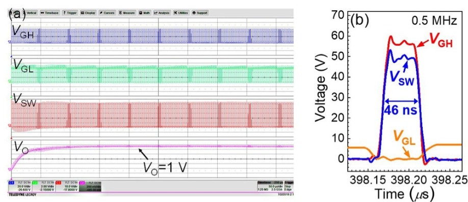
Figure 10. Transient switching waveforms of the 48 V-to-1 V single-stage buck converter, where the VO gradually stabilised at 1 V, proving the function of the GaN IC, (b) detailed single pulse of the converter, highlighting a narrow pulse width of 46 ns and a low duty cycle of 2.2 percent, which guarantees the high switching frequency of 0.5 MHz
One tremendous opportunity for GaN power ICs is the co-integration of GaN Schottky barrier diodes. Their silicon cousins cannot sustain voltages of more than 200 V. Due to this restriction, the rectifying circuits, power factor correction circuits, and switch mode power supplies that operate at more than 200 V often employ silicon diodes with a p-n junction. That’s not ideal, as the resulting circuits suffer from a high reverse-recovery charge, leading to a high switching loss.
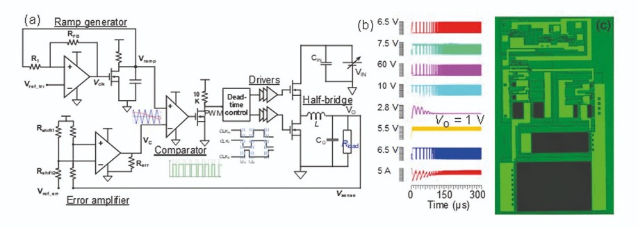
Figure 11. Design of a monolithically integrated all-GaN buck converter comprising half-bridge, drivers, dead-time control, comparator, error amplifier, and ramp generator, (b) simulation waveforms by Cadence based on imec device models and PDK (process design kit), and (c) processed circuit.
- This technology is accessible through the EUROPRACTICE prototyping service.
X. Li et al. GaN-on-SOI: Monolithically Integrated All-GaN ICs for Power Conversion. in IEDM Tech. Dig., pp.4.4.1-4.4.4, Dec. 2019
X. Li et al. IEEE Electron Dev. Lett. 40 1499 (2019)
X. Li et al. IEEE Electron Dev. Lett. 39 999 (2018)
S. You et al., “Monolithically integrated GaN power ICs designed using the MIT virtual source GaNFET (MVSG) compact model for enhancement-mode p-GaN gate power HEMTs, logic transistors and resistors”, pp. 158-161, ESSDERC 2019
GaN-IC Technology, http://europractice-ic.com/mpw-prototyping/power-electronics
Aggressively scaled p-channel GaN transistors, formed on the same epiwafers as their n-type cousins, offer a very promising route to power electronic circuits made with a CMOS technology
BY NADIM CHOWDHURY AND TOMÁS PALACOIS FROM MIT
THE POWER ELECTRONIC CIRCUIT looks set to play an ever-increasing role in all our lives. It is needed in data centres, electric vehicles, cloud computing, and the internet of things.
Often, the performance of this type of circuit is far from ideal. Efficiency is below where it could be, and the circuit takes up much space, due to the use of bulky passive components, such as large inductors and capacitors. What’s needed is to move to more efficient transistors that switch at faster speed. Do this and many benefits result – as well as trimming the electrical losses associated with this device, a higher switching frequency allows the use of smaller passive components that shrink the size and weight of the circuit.
One option for ushering in the era of better circuits is to replace silicon transistors with those made from GaN. Moving to this wide band gap material leads to an increase in the critical electric field strength, making it suitable for high-voltage applications. In addition GaN is renowned for its high saturation velocity, aiding high-frequency operation; and its low on-resistance, enabling low switching losses.
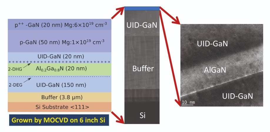
Figure 1. The designed epilayer for p-FETs, along with a transmission electron microscopy image. The structure is as follows: 20 nm p++-GaN (Mg: 6×1019 cm-3 with 2–3 percent activation at room temperature), 50 nm p-GaN (Mg: 1019 cm-3), 20 nm unintentionally doped GaN (Si: 5×1016 cm-3), 20 nm Al0.2Ga0.8N (Si: 5×1016 cm-3), 150 nm unintentionally doped GaN (Si: 5×1016 cm-3), 3.8 μm buffer and silicon substrate.
A major road block towards realising such a technology is the sub-par performance of the GaN p-FET. Compounding this issue, it’s also not easy to find a way to deliver on-chip integration of this device with its partner, an E-mode n-FET. But at MIT we have succeeded on both fronts. Efforts in our lab have culminated in an E-mode p-FET that is easy to integrate with an E-mode, n-type counterpart. The E-mode p-FET delivers great performance, sporting a record low on-resistance, and it produces E-mode operation with a threshold voltage of -1 V .
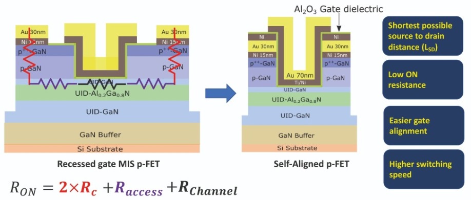
Figure 2. The self-aligned p-FET pioneered by MIT has several advantages over the recessed gate MIS p-FET.
A metal with a very high work function is needed to form a good ohmic contact for the holes in GaN. Nickel oxide is a good choice, due to its work function of around 6.3 eV. By using this oxide, we ensure a relatively good ohmic contact to the two-dimensional hole gas.
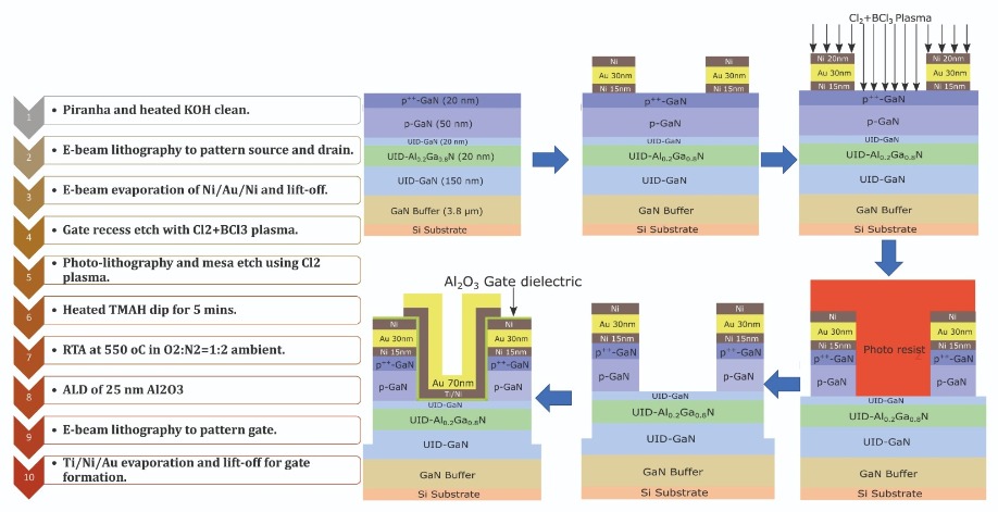
Figure 3. Key process steps for realising the self-aligned p-FET, along with illustrations for each step.
Increasing the hole mobility from 40-10 cm2 V-1 s-1 is far from easy, due to the high effective mass for holes in GaN. Rather than trying to tackle this daunting issue head-on, we simply aggressively scale the device to reduce the transit time of holes from source to drain.
Fabricating pFETs…
To avoid any complications that come from regrowth technology, we use an epilayer design that facilitates both n-FETs and p-FETs. We have undertaken extensive device simulations with TCAD to determine the exact dimensions and the compositions of the layers in this heterostructure (see Figure 1), which we have produced by MOCVD on a 6-inch, 1 mm-thick silicon (111) substrate.
One of the features of this design is the provision of a source of p-type carriers from the polarization-induced two-dimensional hole gas at the interface of the top unintentionally-doped GaN/AlGaN heterostructure. To enabled good ohmic contact to this hole gas, we use a heavily p-doped top GaN layer; and to increase hole mobility, we include a 20 nm-thick unintentionally-doped GaN layer to separate the p-GaN and AlGaN layers. Hall measurements suggest these schemes are successful, as the two-dimensional hole gas density and the drift mobility are 8×1012 cm-2 and 11 cm2 V-1 s-1.
We are not alone in developing a p-type GaN FET. However, while most groups have pursued recessed gate MISFET structures (see Figure 2), we have directed our efforts at a self-aligned architecture. In our view, it has the upper hand on three fronts: it has the shortest possible source to drain distance, cutting down the access region; it has a low on-resistance, thanks to a negligible access resistance; and it simplifies gate alignment.
To produce FETs from our epiwafers, we begin by using electron beam lithography to create source and drain electrodes. Electron-beam evaporation adds a metal stack – 20 nm of nickel, followed by 30 nm of gold and another 20 nm of nickel – prior to a lift-off step using acetone. After this, we use an inductively coupled plasma, reactive-ion etch (ICP-RIE) to provide a blank etch, a step that helps with the formation of the gate recess. During this etch, the top 20 nm-thick film of nickel on the source and drain metal serves as a mask, protecting the ohmic contact from damage. The etch depth is controlled by the etch time. Following this, the mesa etch is performed by an ICP-RIE process, using a photoresist mask and a combination of chlorine and boron trichloride gases.
After all these etching steps, we remove the photoresist and reduce the etch-induced roughness by dipping the sample into heated tetramethylammonium hydroxide for about 15 minutes. We then add about 30 nm of Al2O3 by atomic layer deposition, to create a gate dielectric. Finally, using electron-beam evaporation and lift-off, we form a gate metal electrode, comprising 10 nm-thick titanium, 20 nm-thick nickel and 100 nm-thick gold (note that our entire process is summarised in Figure 3). We have imaged a cross-section of this fabricated device with a scanning transmission electron microscope (see Figure 4).
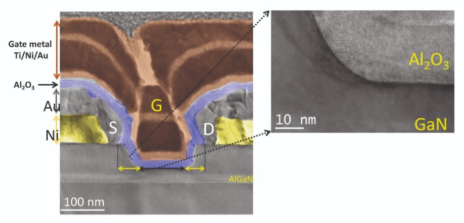
Figure 4. Transmission electron microscopy (TEM) image of the fabricated self-aligned p-FET with a 100 nm channel length. A zoomed TEM image shows the smooth interface between the GaN and gate dielectric, attesting to the high quality of the gate recess process with low surface roughness.
Our p-FETs have an on-off ratio of 6×10⁵ and gate leakage that is typically just 1 nA/mm (see Figure 5(a)). In the off-state, the drain leakage current of these transistors is limited by gate leakage. This leakage is high in the off-state, due to high electric fields between gate and drain terminals, and across the gate dielectric at the sidewall of the gate recess.
The E-mode operation of our FET is seen in the plots of the drain-source current as a function of gate-source voltage (see Figure 5(b)). These measurements reveal a threshold voltage of -1 V. When transconductance is graphed as a function of gate-source voltage, maximum transconductance is shown to be 0.9 mS/mm at -4 V, for a drain-source voltage of -1.5 V. Measuring the output characteristics reveals good pinch-off and an on-resistance of about 400 Ω mm.
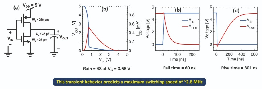
Figure 5. (a) Semi-log plot of IDS vs VGS at VDS=−0.5 V, demonstrating an on-off ratio of 6×10⁵. In the on-state, the gate leakage current is only in the range of 1 nA/mm. However, an increase in gate leakage is observed in the off-state, mainly due to the high electric field at the drain-end of the transistor. (b) Linear scale plot of IDS vs VGS, demonstrating a threshold voltage of −1 V. (c) Measured gm vs VGS characteristics with a peak transconductance of 0.9 mS/mm. (d) Measured IDS vs VDS characteristics, demonstrating an on-resistance of 400 Ω·mm at VGS=−7 V (this is calculated by taking an inverse slope in the low VDS regime of the output characteristics). The plot also shows an on-current density of more than 5 mA/mm at VGS=−7 V and VDS=−5 V.
When comparing various results, it should be remembered that our p-FET has the additional advantage of having a two-dimensional electron gas beneath the two-dimensional hole gas − this holds the key to making an on-chip n-channel transistor with the same epi-structure, without having to resort to any regrowth. When evaluating these transistors, it also important to bear in mind that our p-FET shows E-mode operation, unlike many devices reported in the literature so far.
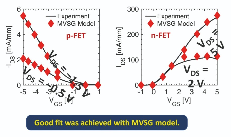
Figure 6. Benchmarking of the reported self-aligned p-FET with other demonstrated p-FETs in the literature in terms of on-resistance and on-off ratio. It is quite evident that the reported device is closest to the desired region exhibiting an on-resistance of 400 Ω mm with excellent on-off ratio of 6×10⁵. The p-FET produced by MIT enables easy integration with an on-chip n-FET without any regrowth, as illustrated in Figure 7(a). The device is E-mode with −1 V threshold voltage. MIT’s FET shows record on-resistance and on-off ratio for any GaN-based E-mode p-FET, making it a promising candidate for GaN-based complementary logic.

Figure 7. (a) Monolithic integration of a self-aligned p-FET and p-GaN gated n-FET. (b) IDS vs VGS characteristics of the n-FET, using in linear scale. This reveals a threshold voltage of 0.2 V. (c) IDS vs VDS characteristics of the n-channel FET.

Figure 8. Compact modelling of both a p-FET and an n-FET using an MIT Virtual Source GaN-FET model yields a good fit with experimental results.
We have studied the switching behaviour of the inverter by applying a capacitive load of 35 pF. The rise time is just 60 ns, far shorter than the fall time of 301 ns, which is compromised by the high on-resistance of the p-FET. However, this fall time is still short enough to yield a switching speed of 2.5 MHz, which is sufficient for most power electronic applications.

Figure 9. (a) Circuit diagram and methodology used in MIT’s simulation of the GaN-based complementary logic inverter. (b) Voltage transfer curve of the GaN-based complementary logic inverter. The n-FET and p-FET have gate widths of 25 μm and 250 μm, respectively. Simulated waveforms showing the (c) fall and (d) rise edge of the output signal from the inverter. The rise/fall time of the input signal is 10 ns. The fall and rise times of the output signal are 60 ns and 301 ns, respectively.
N. Chowdhury et al. “First Demonstration of Self-Aligned pFET on Si”, IEEE International Electron Device Meeting, 2019
N. Chowdhury et al. IEEE Electron Device Lett. 41 (2020) DOI:10.1109/LED.2020.2987003
N. Chowdhury et al. IEEE Electron Device Lett. 40 1036 (2019)
N. Chowdhury, “p-Channel gallium nitride transistor on Si substrate,” Masters diss., Massachusetts Institute of Technology, 2018
High-performance front-ends for millimetre-wave 5G require powerful and efficient GaAs ICs that are housed in carefully chosen packages
BY LIAM DEVLIN, ANDY DEARN, STUART GLYNN, GRAHAM PEARSON, ROBERT SMITH AND MOHAMMED TAHIR FROM PLEXTEK RFI
TO ADDRESS the growing demand for higher data rates and increased capacity, the latest generation of cellular communications is expanding its spectrum usage to include millimetre-wave frequency bands. This move has its pros and cons: it opens up significant opportunities for the compound semiconductors industry, but creates considerable challenges for designers of front-end ICs for 5G applications.
Our team at Plextek RFI (PRFI) is taking on these challenges as we play our part in the roll-out of millimetre-wave 5G. Our efforts include designing and realising a number of custom GaAs ICs, and measuring their performance. Here we detail this work and discuss the challenges of implementing packaging at millimetre-wave frequencies using low-cost surface-mount technology (SMT), and the techniques that can be adopted to ensure the high-performance packaged parts.
Working with GaAs
Millimetre-wave power amplifiers (PAs) based on GaAs technology provide a much higher power density than silicon technologies, as well as a superior power-added efficiency. Using a 0.15 μm gate length E-mode PHEMT process from WIN Semiconductors, we have designed a 28 GHz PA, which we assembled into a 20-pin 4 mm x 4 mm over-moulded plastic QFN (quad-flat, no-leads) package (see Figure 1). To assess its performance, we mounted this packaged PA on a representative evaluation PCB.
The PA in this package is a three-stage design. Its output stage comprises four identical transistors, configured with a power-combining matching network at the output. Such an approach is essential at millimetre-wave frequencies. While in theory, as a transistor is made larger – either by adding more gate fingers or increasing the unit gate width – there is a proportional rise in RF output power capability, in practice this simple approach cannot be adopted at higher frequencies. The problem is that as size increases additional parasitics kick-in at higher frequencies, compromising available gain. So a sweet spot must be found size-wise to balance the competing requirements for gain and RF output power.
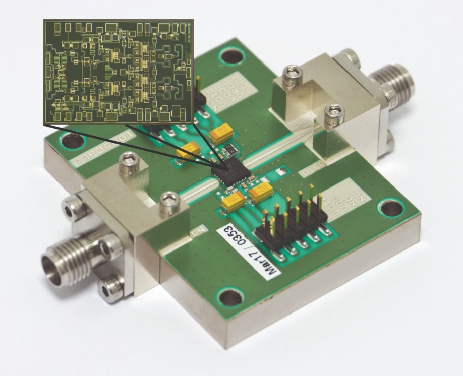
Figure 1. A surface mount technology (SMT) packaged 28 GHz 5G PA that has been developed by PRFI and mounted on an evaluation PCB. A power-combining output-matching network is visible to the right hand side of the die photograph.
We use output power sampling with temperature compensation to allow measureement of the transmitted RF power. We drive the four output transistors with a pair of driver devices, which are in turn are driven with a smaller pre-driver. One of the merits of selecting an E–mode process is that the gates are biased with a positive voltage, so there is no need for a negative supply voltage as required by most D-mode pHEMT PAs. We bias the entire PA from a +4 V drain supply.
A fast-switching enable circuit is also included on-chip. It can be used to rapidly power up and power down the PA. By drawing just 0.1 mA when not in use, it helps maximise overall system efficiency.
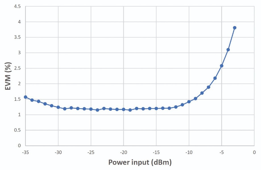
Figure 2. Error vector magnitude (EVM) of the packaged PRFI PA versus PA input power at 28 GHz, OFDM 400 MHz, 64 QAM. At an operating point of 18 dBm average output power, the input power is -3 dBm and the EVM is less than 4 percent.
Like the majority of PAs employed in a 5G communications system, we operate our design backed-off from compression, so that we can preserve the modulation fidelity of the transmitted signal. This is accomplished with a deep class AB bias scheme. Our design efforts begin by selecting the optimum transistor size for the output stage. After this, we simulate load-pull conditions to determine the optimum impedances for best linearity and power-added efficiency at back-off, considering different quiescent bias conditions. Evaluation of the gain, linearity and power-added efficiency follow, enabling us to determine the optimum bias condition. Measurements reveal good performance across the 28 GHz 5G band that spans from 27.5 GHz to 28.35 GHz, using biasing that ensures a 180 mA total quiescent current from +4 V. For this PA the small signal gain is above 20 dB, and the input return loss exceeds 16 dB across the entire band.
We have designed this PA for optimum third-order intermodulation performance and power-added efficiency when backed off by 7 dB below the +25 dBm output power 1 dB compression point; such conditions are close to those that we would expect to be used in a 5G system incorporating this amplifier. According to our measurements, power-added efficiency at P-1dB is around 25.5 percent, rising to 30 percent at the top of the band, and the efficiency of the packaged part at the operating point is 8 percent. While this may not appear to be an impressive result, it is competitive performance for a class AB amplifier operating at this level of back-off.
Another measurement that we have carried out is a two-tone intermodulation test at +18 dBm output. This revealed a level for a metric referred to as the third-order intercept point (OIP3) of +32.5 dBm for an IMD3 of -35 dBc.
The performance of our PA has also been evaluated using a real wideband 5G signal: a 400 MHz bandwidth OFDM signal that has sub carriers every 120 kHz running 64QAM, and a peak-to-average ratio of 11.7 dB. When the PA is transmitting this signal, it has a high degree of linearity, which is evident from a plot of the error vector magnitude against input power at 28 GHz (see Figure 2).
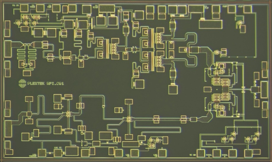
Figure 3. Die photograph of a PRFI 28 GHz front-end module (FEM). The PA runs from left to right along the top of the die photograph, and the Tx/Rx switch can be seen in the centre right of the die. The low-noise amplifier (LNA) runs from right to left, with RF output towards the bottom of the left-hand edge of the die.
Perfecting the package
In consumer electronics, surface mount technology (SMT) dominates the assembly process. Consequently, if millimetre-wave 5G components are to be commercially successful, they must be available in SMT-compatible packages. The most common, lowest-cost form of this for microwave and millimetre-wave components is over-moulded plastic, used for the 28 GHz PA that we have described (shown in Figure 1). For this amplifier, the style is QFN, which is the most popular SMT package for microwave ICs. It features a solid metal base, which is solder-attached to a ground plane on the PCB. Merits of this include a good thermal contact and a low inductance contact to PCB ground.
If an IC is designed for best performance as a die, with no consideration given to packaging, and this chip is assembled into a package – even one with a style already used effectively for millimetre-wave ICs – the performance is severely degraded. To ensure that the package does not hamper performance, there is a need to carefully consider the impact of: the moulding compound in direct contact with the surface of the IC; the inductance of bondwires, and the transition from the die through the package to the PCB; the physical size of the package leadframe, which has the potential to be resonant in-band; and the grounding inductance between the IC ground and the PCB ground.
During the design process, we use electromagnetic simulations to evaluate the impact of the moulding compound. Ultimately, it is the performance of the packaged IC on the PCB that is of most importance, so the design must be optimised for this. Many available IC processes include a passivation layer on the surface of the die that mitigates the effects of the plastic. Other options for housing the PA include air-cavity plastic packages and other forms of SMT that have an air cavity, such as laminate, ceramic or liquid crystal polymer. Although all are available as standard ‘open-tooled’ packages, custom designs can be used to optimise the performance of a particular IC.
We know that the inductance of the bondwire can severely degrade the performance of a millimetre-wave IC. Our first step to minimising the impact of this inductance is to trim the length of the bond interconnect, by co-designing the IC and package. Further reductions in inductance result from using multiple bondwires: our packaged millimetre-wave ICs tend to have two or three bonds to the RF pads. As well as taking these steps, we incorporate the series inductance of the bondwires into a low-pass filter that also comprises the capacitance of the RF pad on the IC, the series inductance of the package lead, and the capacitance of the package SMT pad to the PCB ground.
The 5 mm x 5 mm packages that we use have a corner-to-corner distance of just over 7 mm. This gives rise to a potential for resonance at 21.4 GHz – the frequency that corresponds to half a wavelength in air. The presence of moulding compound increases the effective electrical dimensions, leading to a lower resonant frequency. Due to this, there is a danger that the physical size of the package will result in an in-band resonance at millimetre-wave frequencies. To prevent this, we use an appropriate design for the custom leadframe, with selected pins directly connected to the die attach paddle. In addition, we give much thought to the design of the PCB on which the packaged IC is mounted.
For ICs made from GaAs and GaN, the backside of the chip is normally the RF ground. A low-inductance connection to this is made with the die attach paddle in the QFN style package. Using this approach, the exposed paddle on the back of the package is normally connected to the PCB ground.
When adopting this approach, it is vital to ensure a sufficiently low inductance for the IC to PCB ground connection. Much consideration must be given to the grounding inductance, as it is a source of series inductive feedback around the IC. If this inductance is too high it degrades performance – and in the worst case, it even causes instability. This can be avoided by using thin substrate material and multiple connections from the paddle to PCB ground.
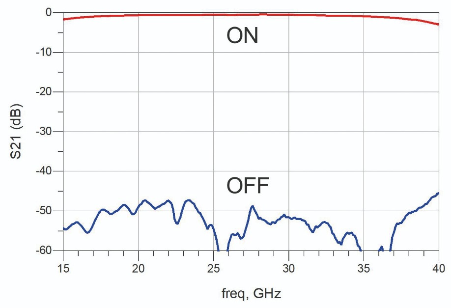
Figure 4. RF on-wafer measured on-state and off-state performance of a typical switch.
Packaging front-end modules
We have also used GaAs technology to design more highly integrated front-end millimetre-wave components. They include a front-end module for the 28 GHz 5G band comprising a three-stage PA, RF transmit power detector, Tx/Rx switch and two-stage low-noise amplifier (see Figure 3). Again, this IC has been designed using WIN’s 0.15 μm gate length E-mode pHEMT process that was used for the PA, and has been housed in a 5 mm by 5 mm over-moulded plastic QFN package.
One can view the PA in this front-end IC as essentially half of the PA MMIC described above. That is, rather than four transistors for the output stage, there are two. It thus has around half the RF output power capability of the MMIC with four transistors, but offers a similar level of gain. It also features a temperature-compensated RF output power detector.
In this module, the Tx/Rx switch connects the RF common port of the IC to either the PA output or the low-noise amplifier input. By arranging multiple switching transistors in a cascade configuration, power handling improves, and linear operation is ensured at the desired RF output level.
To bring the point of optimum noise match closer to the point of best return loss, we use series inductive feedback in the low-noise amplifier. A stacked bias scheme is adopted, with the same DC current running through both transistors to provide an Rx path gain of 13.5 dB with a supply current of just 10 mA from a +4 V source.
For the transmit path, output power is just over 20 dBm at 1 dB gain compression, with a power-added efficiency of 20 percent. These figures come from measurements on a packaged part that is assembled onto a representative evaluation PCB. Design has been optimised for high efficiency, when backed-off for linear operation with an IMD3 of -35 dBc. Using a 100 MHz tone spacing, OIP3 is around +28 dBm across the 5G band. There is very little variation with tone power over a 10 dB dynamic range.
Additional measurements reveal that the receive path gain is 13.5 dB and the noise figure 3.3 dB. This path has impressive linearity – OIP3 is 20 dBm, for a DC power consumption of just 40 mW.
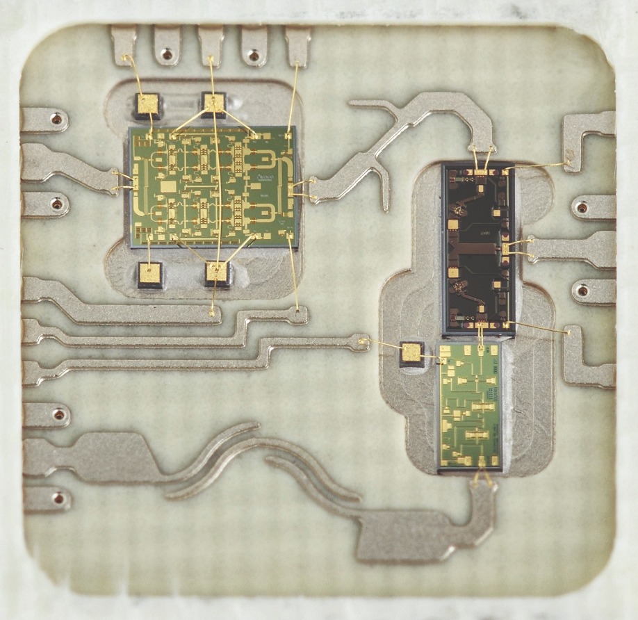
Figure 5. A 26 GHz 5G front-end, multichip module designed by PRFI and housed in a custom laminate package. The PA is the largest die, seen in the top left of the photograph. The Tx/Rx switch is to the centre right of the photo, the common RF Tx/Rx port is to the right of the switch die on the centre right edge with its ground-signal-ground through-package transition clearly visible. The Tx port of the switch connects to the harmonic filter at the top of the switch die and the Rx port at the bottom of the switch die connects directly to the low-noise amplifier input.
Low-loss MMIC switches
Most commercially available RF and microwave switches are based on FETs, produced using either pHEMT or SOI processes. Unfortunately, as the operating frequency increases, it becomes ever-more challenging to design this class of switch. The biggest issue is that although the drain-source resistance of the FET is high when pinched-off, there is a parallel parasitic capacitance that becomes significant at higher frequencies, offering a low-impedance path to RF signals. One option for trimming this capacitance is to turn to smaller transistors, but this produces a hike in on-state loss, and power handling is compromised.
Instead, we advocate the use of p-i-n diode switches for millimetre-wave applications. One of their best attributes is that, for a comparable on-state resistance, they provide a much lower parasitic off-state capacitance than FETs. This leads to a low insertion loss and high isolation at millimetre-wave frequencies. Another merit of the p-i-n diode is that it behaves as a current-controlled resistor at RF and microwave frequencies. As this class of diode can also be optimised to provide a wide resistance range, good linearity and high-power handling capability, it is an excellent choice for making RF and microwave switches.
Although the off-state capacitance of the p-i-n diode is very low, it can still represent a significantly low reactance at millimetre-wave frequencies. For example, if the off-state capacitance is just 0.05 pF, this would reduce the isolation of a series-mounted off-state device to just 3.6 dB at 28 GHz. To ensure high isolation, we use shunt mounted diodes to provide a low-resistance path to ground in the on-state. When series and shunt diodes are combined, the broadband switches that result can span from near DC to millimetre-wave frequencies. If operation down to such low frequencies is not required, then switches can be built using just shunt devices. A bandpass response results, but with the advantage of lower insertion loss at millimetre-wave frequencies, thanks to the absence of series devices.
We have designed SPDT, SP4T and DPDT millimetre-wave switch MMICs using p-i-n diode processes. Taking RF on-wafer measurements allows us to compare on-state loss with off-state isolation for a SPDT switch that has two shunt-mounted p-i-n diodes in each arm (see Figure 4). When the diodes are ‘on’ they provide a low resistance to ground and a high isolation through that branch; and when they are ‘off’ they have a small shunt capacitance, which is absorbed into a low-pass filter, resulting in a low insertion loss through that branch. Our RF on-wafer measurements reveal an on-state loss of just 0.55 dB ± 0.1 dB across the 20 GHz to 32 GHz range, with isolation exceeding 47 dB.
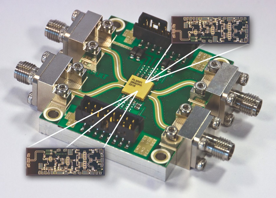
Figure 6. PRFI’s dual-channel 26 GHz PA in custom laminate package. The measured S22 of the packaged part improves at the top of the band compared to the bare die. S22 is less than -12.5 dB from 24 GHz to 28 GHz. The S11 degrades slightly compared to the bare die, but is still less than -10 dB.
Multi-chip modules
Another class of design is a millimetre-wave multi-chip module, made with surface-mount technology and formed using laminate packaging. Using this approach, we have created a multi-chip front-end module housed in a 10 mm x 10 mm laminate QFN package (see Figure 5). Manufacturing and assembly have been undertaken by Filtronic, UK.
The multi-chip module includes three commercially available die: a p-i-n diode SPDT Tx/Rx switch, a pHEMT low-noise amplifier and a pHEMT PA. There is also a pair of single-layer capacitors, positioned either side of the PA, which provide supply decoupling. The output of the PA is routed through a harmonic filter, which is printed on the base of the laminate package and fabricated as an integral part of the package. This filter provides more than 20 dB of harmonic rejection, and its insertion loss is just 0.2 dB.
The module includes a receive bandpass filter, integrated into the package base at the output of the low-noise amplifier. This filter is a coupled-line structure, which has adopted a curved shape to fit into the available physical space; it has an insertion loss of 0.7 dB. Measurements of this front-end module, which has been mounted on a PCB, show good agreement with simulations. Receive path gain is 20 dB, and the noise figure is around 3.5 dB. Transmit path gain is 19 dB, and the OIP3 is +36 dBm.
Dual channel amplifiers
In order to address the difficulties of non-line-of-sight communications in the millimetre-wave domain, 5G mobile terminals will adopt either a phased array or a switched antenna topology. Both options require the use of multiple, identical RF front-end components, such as PAs. These amplifiers must fulfil many criteria – they need to deliver adequate gain, output power and linearity, while being efficient, compact and low cost. One solution for making the multi-channel millimetre-wave PAs is to realise multiple PAs on a single die (we shall discuss this later in this article) and an alternative is to co-package multiple, single-PA die.
An example of the latter approach is our dual-channel PA in a custom laminate surface mount package that has two RF inputs and two RF outputs (see Figure 6). This PA MMIC produces 22 dB of gain across the 24 GHz to 28 GHz band with an RF output power of 26 dBm at P-1dB and a power-added efficiency of 30 percent. Housing the MMIC is a package that has a standard 32-pin QFN footprint with a solid copper base and a 7 mm by 7 mm body; it is attached to a representative evaluation PCB. We have developed this unit in collaboration with Filtronic, which provided package manufacture and assembly.
Encouragingly, the s-parameter measurements of both channels of the packaged dual-channel PA are very similar to the corresponding on-wafer measurements. This underscores the quality of the die to PCB transition offered by the custom designed package. Measurements of the packaged PA at -40 °C, +25 °C and +85 °C reveal that the gain variation with temperature is around 0.04 dB/°C. There is a very modest variation in input and output match with temperature. The measured OIP3 of the packaged PA is typically around 36.5 dBm at both room temperature and -40 °C, and drops by around 1dB at high temperature.
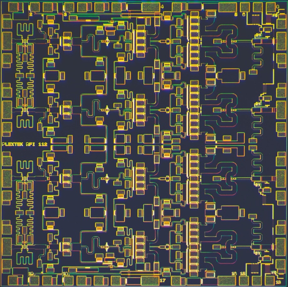
Figure 7. Die photograph of a PRFI 4-channel 28 GHz PA.
Four-channel, single-chip PAs
We have also designed a single-die, four-channel MMIC that covers the 28 GHz 5G band (see Figure 7). The ICs have been fabricated with Sanan IC’s P15EP process – a 4 V, 0.15 μm, enhancement-mode GaAs pHEMT process – and housed in a standard 5 mm by 5 mm plastic over-moulded QFN package. To benchmark performance, this package has been mounted on a representative evaluation PCB.
Each of the four PAs is a three-stage design that includes its own independent RF output power detector. For each channel, measured gain is 19.6 dB ±1.4 dB across 26 GHz to 29 GHz, and input and output return losses are 10 dB across the band. Although the PAs for 5G systems will be operated backed-off from compression, to provide a figure-of-merit to aid comparison, we have measured the RF output power at 1 dB gain compression. This gave a figure of 24.5 dBm, and a corresponding power-added efficiency of 19.5 percent. Values for saturated output power and corresponding power-added efficiency are 25.5 dBm and 21.5 percent.
If all four PAs are driven with coherent RF signals and deployed in a suitable four-element antenna array, the RF output signals will combine to provide an additional 6 dB in RF power over a single channel. By adjusting the phases of the signals to the four antenna elements, the direction of the beam can be steered electronically. As the gain of each antenna element also adds to the total effective isotropic radiated power, this approach increases the effective RF power and the range of the communications link.
The designs we have developed underpin the huge opportunity that the compound semiconductor industry has through the addition of millimetre-wave frequency bands to the 5G communications standard. Through innovation in device design, and careful selection of the packaging, there is much opportunity for market success.
Closing the Gap between Measured and Modelled MMIC Performance - PRFI White Paper: https://www.plextekrfi.com/wp-content/uploads/accurate_simulation_of_mmics.pdf
L. Devlin “A guide to SMT packaging of Microwave ICs” proceedings of the ARMMS RF and Microwave Society Conference, November 2012: https://www.plextekrfi.com/wp-content/uploads/Guide_to_ SMT_Packaging_of_Microwave_ICs.pdf

Curved mirrors and a longer cavity combat overheating in green-emitting VCSELs
ENGINEERS AT SONY have fabricated a green-emitting VCSEL that produces continuous-wave emission at room-temperature. By overlaying its emission with that from red and blue VCSELs, the researchers claim to have produced the first ever full-colour light source from this class of laser.
According to the team, the VCSEL’s high level of directivity, along with its very low power consumption, promises to enable it to set a new benchmark for efficient delivery of visible light. Applications that could benefit include retinal scanning displays.
Sony is not the first producer of green VCSELs. In 2016, a team from Xiamen University, China, reported quantum-dot VCSELs emitting in the blue, green and yellow. These devices had an incredibly low threshold current of below 1 kA cm-2. However, according to the team from Sony, wavelength emission stability is a challenge with this design, due to inconsistencies in quantum dot quality and instability in controlling the cavity length. Another issue, which inhibits beam formation, is filament lasing – it is thought to stem from the spatial inhomogeneity of the dots.
To avoid these pitfalls, Sony’s engineers have developed a green-emitting VCSEL that has quantum wells and employs an architecture that addresses another concern – a thermal blockage in the bottom mirror that threatens to cause the chip to overheat.
With Sony’s solution, a far longer cavity combats thermal resistance. Lengthening the cavity might increase diffraction loss and ultimately prevent lasing, but this is avoided by incorporating curved mirrors.
Another impediment to the performance of a green VCSEL is the high electric field in the active region. This pulls apart electrons and holes, leading to a higher threshold current. To tackle this issue, Sony’s engineers use a semi-polar substrate for the growth of their emitting region.
Fabrication of Sony’s VCSEL began by loading {2021} GaN substrates into an MOCVD reactor and depositing four quantum wells, a p-doped GaN layer, and a p-type contact layer. On this 130 nm-thick heterostructure the team added a 30 nm-thick layer of indium tin oxide, and then a p-side DBR of alternating layers of Ta2O5 and SiO2, designed to have a peak reflectivity at 515 nm. Etching and the deposition of electrodes followed, to produce an aperture and a current-injection region.
After this, the engineers lapped the wafer to a thickness of about 20 μm, before photolithography defined 26 μm-diameter resin discs. Heating the sample to 200 °C melted the discs into droplets, before reactive-ion etching transferred their shape onto the GaN, to create a lens-shaped surface. The addition of 14 alternating layers of Ta2O5 and SiO2 formed curve mirrors, before dicing and mounting in a package completed the fabrication process.
Measurements of the green VCSEL revealed a threshold current of 1.8 mA, and a wall-plug efficiency below 0.1 percent.
As the current increased from 5 mA to 6 mA, the emission peak switched from 515 nm to 518 nm.
This 2.7 nm hop is consistent with a cavity length of 18.6 μm, and the expected values for the refractive index of GaN and its change with wavelength.
Far-field images of the emission show a single peak that can be fitted with a Gaussian curve. This emission corresponds to an emission spot size of 2.4 μm to 2.6 μm.

Retinal scanning displays could benefit from efficient, low-power, full-colour light sources made from red, green and blue VCSELs.
T. Hamaguchi et al. Appl. Phys. Express 13 041002 (2020)

UV emitters are set to benefit from high-quality, semi-polar templates formed by an ammonia-free growth process
LIKE GREEN LEDs, those that emit in the deep UV are impaired by internal electric fields that hamper radiative recombination and produce a red-shift in emission.
To address these concerns, Xu-Qiang Shen and co-workers from the Advanced Power Electronics Research Centre in Tsukuba, Japan, have developed high-quality, semi-polar AlN templates for the growth of UV LEDs.
“We have successfully obtained high-quality, semi-polar AlN without observable twins and basal-plane stacking faults by the relatively simple, ammonia-free, high-temperature MOCVD growth method,” explains Shen.
This success breaks new ground, as previous efforts failed to produce semi-polar AlN with sufficient material quality for making high-efficiency devices.
Instrumental to the breakthrough by the team has been the use an ammonia-free growth process. Theoretical simulations hinted at the benefits of replacing ammonia with nitrogen, before experimental work validated the switch.
Shen argues that avoiding ammonia has several advantages: it prevents pre-reactions, associated with adduct formation; it allows fast growth at high temperatures; it simplifies abatement equipment; it trims running costs; and it results in a more environmentally friendly process.
Growth of the semi-polar templates is not realised in a commercial reactor. “We use a specially designed MOCVD system, which is very simple,” says Chen.
He and his co-workers load m-plane (1010) sapphire substrates into the reactor, and add a film of (1013) AlN at 1650 °C at a growth rate of typically 1.2 μm/hr. Sources for the growth are nitrogen and trimethylaluminium, transported to the chamber using hydrogen as a carrier gas.
X-ray diffraction measurements on the sample with a 2.3 μm-thick film of AlN produce two peaks – one is for (1013) AlN, and the other for (3030) sapphire. This implies that single-phase epilayers of (1013) AlN have been grown on m-plane (1010) sapphire substrates.
One of the dangers when growing AlN on sapphire is that the two equivalent {1120} planes in the substrate lead to the growth of twins in the epilayer, resulting in a rough surface morphology that is incompatible with the production of high-quality devices.
To see if their sample had been compromised by any twins, Shen and his colleagues undertook high-resolution X-ray diffraction, using a carefully selected orientation of their sample. Scans failed to find any evidence for twins in their semi-polar AlN film.
Additional X-ray scans produced diffraction peaks for the (1013) and (0002) directions of 322 and 373 arcsec, respectively. According to the team, these values, which provide an indication of material quality, are even better than those of “top-class” AlN epilayers on c-plane sapphire.
Atomic force microscopy scans of a 5 μm by 5 μm area show that the surface roughness is about 2 nm. The scans also reveals stripes with a height of around 5 nm, thought to stem from the off-cut angle of the substrate – it is 2.0 °.
To scrutinise the AlN epilayer for microstructures, the team have used cross-sectional scanning tunnelling electron microscopy in dark-field mode, analysing the sample in two perpendicular directions. Images reveal dislocations propagating to the surface, and voids at the interface between the substrate and epilayer (see figure).
Plans for the team include improving the growth technique and epilayer quality, and using the AlN epilayer as a template for making devices. “We are looking for co-operation for further development,” says Shen.
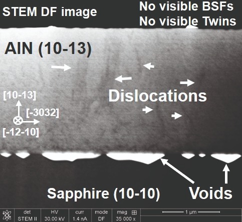
Cross-sectional, scanning tunnelling electron microscopy images obtained in dark-field mode of the semi-polar AlN indicate its high-quality. There are no twins or basal stacking faults.
X.-Q. Shen et al. Appl. Phys. Express 13 035502 (2020)

Replacing the SiN passivation layer with thick, epitaxially grown AlGaN eliminates dispersion in polarisation-graded FETs
ENGINEERS from The Ohio State University and Qorvo have refined the design of the polarisation-graded FET, a promising device for power amplifiers in 5G millimetre-wave base stations. To eradicate interface traps that are to blame for dispersion, they replace the SiN passivation layer with thick epitaxial AlGaN.
Spokesman for the team, Shahadat Sohel from The Ohio State University, says that they are the first to report DC-RF dispersion-free behaviour up to an extreme high quiescent bias condition in a high-power, high-linearity AlGaN channel transistor. “DC-RF dispersion is one of the main reasons for low output power in any transistor.”
Polarisation-graded FETs are attractive alternatives to GaN HEMTs, the leading technology in high-frequency base stations, because they have a far flatter transconductance profile that enables greater linearity.
The superiority stems from the incorporation of a three-dimensional electron gas, formed by linearly grading the aluminium composition in the channel. With a three-dimensional gas, variations in bias have minimal impact on the volumetric carrier density – and in turn, changes in gate voltage produce only small variations in the electron saturation velocity, leading to better linearity.
Sohel and co-workers did not invent the polarisation-graded FETs. “But we optimised and improved the design to achieve record linearity performance for X-band application.”
Fabrication of the team’s FETs began by loading a SiC substrate into an MOCVD chamber and depositing a GaN buffer, followed by: a 20 nm-thick AlGaN channel with an aluminium content that is linearly graded from 0 percent to 30 percent; and an epitaxial passivation region consisting of a 20 nm-thick graded barrier taking the composition from Al0.3Ga0.7N to GaN, a 20 nm-thick layer of GaN and a 80 nm-thick layer of Al0.2Ga0.8N. Within this heterostructure there is a two-dimensional electron gas at the interface between GaN and Al0.2Ga0.8N that screens the channel from the surface, to ensure that the pinch-off voltage of the access region is more negative than that from the gate region.
Source and drain contacts were formed by etching the cap layers, adding a Ti/Al/Ni/Au stack by electron-beam evaporation, and transforming this into an alloy with rapid-thermal annealing at 850 °C. Formation of the gate began by using chlorine gas to etch a 0.7 μm-wide recess, before turning to MOCVD to deposit a 5 nm-thick SiN film. It acts as a gate dielectric, reducing gate leakage, and also isolates the gate from the two-dimensional electron gas. To complete the fabrication of the Schottky gate, the engineers added a Ni-Au-Ni metal stack.
To create a field plate, Sohel and co-workers employed a 0.3 μm extension of their gate towards the drain. This provides an additional reduction in dispersion by diminishing the peak electric field, as well as increasing the breakdown voltage.
Electrical characterisation revealed a maximum output current of 500 mA mm-1, a flat transconductance with a maximum value of 160 mS mm-1, and a three-terminal breakdown voltage of 110 V for a 3.5 μm spacing between the gate and drain. Analysing the source of the leakage current indicated that the Schottky gate is primarily responsible for the breakdown.
Measurements involving 5 μs pulses with a 0.1 percent duty cycle, a pinched-off gate quiescent bias of 5 V, and a drain quiescent bias up to 50 V, showed minimal dispersion for both current collapse and knee-walkout (this is the increase in knee-voltage). In comparison, polarisation-graded FETs with SiN passivation, reported by Sohel and co-workers in 2018, had a 25 percent current collapse and a 8 V knee-voltage walkout for a 30 V drain quiescent bias condition.
Sohel and co-workers are now developing a sacrificial layer underneath the field plate to reduce parasitic capacitance. “We are also working on scaled gate-length and source-drain spacing to increase the operating frequency of the transistor.”
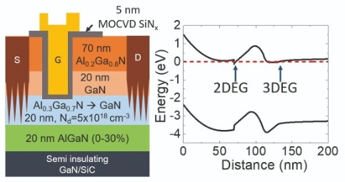
Replacing the SiN passivation layer with AlGaN reduces dispersion from surface states in the polarisation FET.
S. Sohel et al. Appl. Phys. Express 13 036502 (2020)
