
The progress of the silicon IC has been driven by scaling. Increasing the size of the wafers has brought down costs, and shrinking the size of the transistor to the nanoscale has propelled performance, while trimming power consumption.
For the optical equivalent, the photonic integrated circuit (PIC), one can follow in these footsteps. Whether the substrate is silicon or InP, wafer size can increase. And efforts can be directed at shrinking the size of all the components that form the PIC.
However, how much can be gained by making ever smaller features? The nanoscale is fine for electrons zipping through transistors, but is it a good idea for photons with wavelengths beyond a micron?
One company that thinks that it’s important to hit a sweet spot, rather than pursuing ever smaller dimensions with diminishing returns, is PIC manufacturer Rockley Photonics. It makes the case for the design in its feature The benefits of multi-micron waveguides.
According to Rockley, multi-micron waveguides offer several benefits: they deliver a ten-fold reduction in waveguide loss; they slash performance variability by a factor of 25; they provide polarization independence; and they enable the use of a monolithic ultra-broadband fibre-attach technology.
Another benefit of multi-micron waveguides – and this may come to you as a surprise – is that they can realise tight bends while ensuring strong confinement of the electromagnetic wave. That’s a major asset, because designers of PICs want to avoid large bends, so that they can reduce the footprint of these chips.
Rockley employs several foundries for the production of its integrated optical engines. Waveguides and active silicon devices are produced in a fab that processes silicon-on-insulator wafers, and lasers are made in a III-V fab, before being attached directly to a recess etched into a silicon waveguide. The resultant chip is then combined in a package with an IC, made at a foundry offering advanced CMOS and BiCMOS processes.
Rockley is targeting many applications with these packaged products. It is vying for success in the data communications sector, where it can meet requirements for high bandwidth and compactness; and it has a competitive offering for LiDAR, meeting the demand for high-power handling.
I hope Rockley’s PICs enjoy much success. But even if they don’t, they have helped me to stop falling into the trap of thinking that for ICs, smaller devices must be better.


Transphorm has confirmed that customer AES Aircraft Elektro/Elektronik System GmbH has released its first 650 V GaN-based power supplies. Serving the aviation industry, AES supports customers with various products and services ranging from electrical engineering to certification and testing.
The company’s newest switch mode power supplies are currently used by large CS-25 airplane manufacturers
(for example, Airbus A318-A321, A330, A340, A380 and Boeing B767, B787 VIP aircraft) and use Transphorm’s GaN FETs to increase overall system efficiency by more than 10 percent compared to competitive silicon-based power supply units (PSUs).
The two GaN-based switch mode power supplies are the PS250X 500 W system and the PS6120 1200 W system. Both products support a 96-130 VAC/360 Hz - 800 Hz input voltage with a 28 V, DC continuous power output at 15 amps for the 500 W system and 42 amps for the 1200 W system.
Further, AES certified the PS250X and PS6120 as DO-160 compliant – meeting the more than 25-point stringent Standard of the Radio Technical Commission for Aeronautics (RTCA). This Standard assesses system impact and performance under various external and internal conditions on aircraft – ranging from pressure and temperature to voltage spikes and RF emissions.
The flagship 500 W PS250X is the industry’s first passively cooled power supply at 420 W and deploys Transphorm’s GaN in a single-phase CCM boost power factor correction (PFC) topology. It offers more than 92 percent overall system efficiency at full load, which is more than 10 percent greater than its competition. The system also yields a more than 0.98 power factor and 200 mVpp nominal at 115 VAC/400 Hz input at full load. All within an end product that is 1.4 kg.
The 1200 W PS6120 deploys Transphorm’s GaN in a fan-cooled, three-phase CCM boost PFC topology. It offers more than 91.5 percent overall system efficiency at full load, which is 11.5 percent greater than its competition. The PS6120 also yields the same power factor and nominal ripple voltage at 115 VAC/400 Hz input at full load as the PS250X 500 W PSU. All within an end product that is 4.0 kg.
“The aviation industry is working toward reducing climate impact through any means possible,” said Andreas Hammer, Head of Competence Center Power, AES.
“Considering, we sought out Transphorm’s GaN to replace previously used silicon MOSFETs so that we could provide a more efficient, lighter weight power supply. These supplies have the potential to make a notable impact when considering each aircraft deploys several such PSUs. After only a year of redesign, we were able to offer our customers a better power solution, while also raising the performance bar within our own industry.”
Interested in the technology’s inherent higher switching frequency, AES reviewed GaN power switch converters from several GaN device semiconductor manufacturers. The company ultimately selected Transphorm’s 650 V GaN technology due primarily to its ease of drivability and designability – specifically because Transphorm’s GaN FETs do not require custom drivers.
As a result, system design is simplified while engineers can drive the switches using technology they are already familiar with. Other factors affecting AES’ selection included Transphorm’s proven reliability, which is underscored by its GaN platform earning both a JEDEC qualification and AEC-Q101 qualification at 175°C.
“Transphorm designed its GaN devices to enable designers, not challenge them,” said Philip Zuk, VP of Worldwide Technical Marketing and NA Sales, Transphorm.
“Our two-switch normally-off GaN devices come in standard packages and require minimal supporting circuitry to drive them, which reduces the overall system size, increases reliability, and simplifies design. It’s crucial to us that our customers can come to market quickly with a product they have confidence in. We’re honoured to be AES’ GaN supplier of record and are proud that they appreciate the work we’ve done to bring the benefits of GaN technology to the masses.”

Micledi Microdisplays, the latest spin-off of from Imec, has raised €4.5 million in seed capital. The funding will be used to develop microLED displays for next generation Augmented Reality (AR) glasses.
Micledi’s vision is to enable AR for everyday personal use – smart glasses that are small, lightweight, with long battery life, and at reasonable cost. To make this happen, Micledi is developing the world smallest and brightest displays. The key innovation behind Micledi is the new integration technology for microLEDs on 300 mm wafers developed in collaboration with Imec.
Micledi Microdisplays was founded by Soeren Steudel and Alexander Mityashin, both researchers from Imec with a deep know-how in the R&D field and display development. They are joined by Sean Lord, an experienced executive in the semiconductor industry, as CEO. “AR glasses may replace our smartphones in the future and display technology is a key enabler for such a transition.
Today’s display technologies cannot fulfil the specifications needed for next generation AR glasses. At Micledi we are tackling this challenge and have developed displays that are a hundred times brighter than commercial alternatives”, explained Soeren Steudel. In order to implement the vision that future consumer AR devices will be powered by a tiny display developed in Leuven, the company has raised €4.5 million seed investment from Imec.xpand, PMV, and FIDIMEC.
“We are pleased to back a unique team. We look forward to working with them and to enable technology that will be at the core of future AR devices and will change how digital information is presented to consumers,” said Cyril Vancura, Partner at Imec.xpand. Micledi’s will develop its microLED technology and first prototypes on Imec’s 300 mm pilot-line infrastructure. “Hardware development takes courage, capital and time. We are proud of the entrepreneurship of our engineers to bring promising technology developments originating from our R&D, to the market,” said Luc Van den hove, president and CEO at Imec.
“Based on an original concept launched, now more than two years ago, by the Micledi team, Imec together with Imec.xpand incubated this into a promising technology base and exciting business case. It leverages Imec’s extensive R&D in organic displays, 300 mm integration and wafer-scale optics technologies.”
“Micledi’s new generation displays for AR glasses fits in PMV’s strategy of supporting early stage technology with a largescale international potential, hence strengthening Flander’s position as a top region,” said Roald Borré, head of equity investments at PMV.

As projectors grow more and more popular in home entertainment systems, so have the expectations of users. In addition to ever-higher resolutions, the focus is also on richer colours, contrasts and, of course, higher brightness.
With the Ostar Projection Power family, Osram says that it has succeeded for the first time in achieving projector brightness levels beyond the 3,000 ANSI lumen barrier using LEDs instead of conventional lamps, making them accessible to a broad market.
Depending on the ambient light conditions and the distance to the projection surface, requirements differ for the light source. With 12 new products, Osram is now able to offer three different power classes for RGB solutions in deep blue (440 nm), blue (456 nm), converted green (520 nm) and amber (614 nm).
In the lowest power class, two chips of the same colour per component provide projector brightness of up to 1,500 ANSI lm. In the mid-power class, four chips of the same colour per component can achieve 2,500 ANSI lm. While in the highest power class, six chips of the same colour per LED can achieve more than 3,000 ANSI lm. As a result, products from the Osram Ostar Projection Power family emerge as a clear alternative to the high-pressure discharge lamps previously used in projectors above 2,000 ANSI lm.
This leap in performance was achieved, among other things, by improved chip and package technology. The developers at Osram have fundamentally modified the individual LED chips allowing them to be electrically connected in series on the copper board. The system designer benefits not only from a significantly lower operating current (with the same power consumption) and reduced complexity of the LED driver, but also from the much simpler contacting of the component. In addition, direct coupling of the LEDs to a heat sink is possible – without additional isolation costs.The mechanical design remains largely unchanged compared with previous products enabling a fast and uncomplicated exchange of the products in existing projector systems.
“With products from the Osram Ostar Projection Power family, we have successfully crossed the 3,000 ANSI lumens barrier using LED technology,” explains Wolfgang Schnabel, product manager in the Visualisation & Laser division at Osram Opto Semiconductors. “Our customers can easily integrate the new components in their desired power class into their system design and replace conventional lamps with state-of-the-art LED systems.”
Lumentum, ON Semiconductor, and the AI company Ambarella have announced a joint 3D sensing platform for the development of intelligent access control systems and smart video security products such as smart video doorbells and door locks.
The platform is based on Ambarella’s CV25 CVflow AI vision system on chip (SoC), structured-light powered by Lumentum’s VCSEL technology, and ON Semiconductor’s AR0237IR image sensor. Ambarella, Lumentum, and ON Semiconductor demonstrated the platform during CES 2020.
Traditional structured-light solutions need to use both an infrared (IR) camera and a separate RGB camera and typically, a dedicated ASIC for depth processing. This new platform leverages a single
ON Semiconductor AR0237 RGB-IR CMOS image sensor to obtain both a visible image for viewing and an infrared image for depth sensing. The Ambarella CV25 AI vision SoC powers depth processing, anti-spoofing algorithms, 3D facial recognition algorithms, and video encoding on a single chip, significantly reducing system complexity while improving performance.
“Lumentum has worked to enable diverse applications of our VCSEL technology into next-generation 3D sensing products,” said Andre Wong, vice president, product line management, 3D Sensing at Lumentum. “We are excited to partner with Ambarella to help expand the use of 3D sensing in new applications including video security and more broadly AI vision.”
“ON Semiconductor’s RGB-IR sensor technology enables single sensor solutions to provide both visible and infra-red images in security and vision IoT applications,” said Gianluca Colli, vice president and general manager of the Commercial Sensing Division at ON Semiconductor.
“Ambarella’s CV25 computer vision SoC, with its next-generation image signal processor (ISP), brings out the best image quality of our RGB-IR sensor, while providing powerful AI processing capability for innovative use cases in security applications.”
“We are delighted to partner with Lumentum and ON Semiconductor to deliver a hardware platform for the next generation of intelligent access control systems and video security devices,” said Fermi Wang, president and CEO of Ambarella. “Powered by Lumentum’s VCSEL solution, ON Semiconductor’s RGB-IR technology, and our CV25 SoC, it delivers 3D sensing with reduced system complexity as well as improved reliability and security. We look forward to seeing the innovative products our customers will build with this hardware platform.”
Ambarella’s CV25 chip includes a powerful ISP, native support for RGB-IR colour filter arrays, and advanced high dynamic range (HDR) processing, which results in exceptional image quality in low-light and high-contrast environments.
CV25’s CVflow architecture delivers the computational power required for liveness detection and 3D face recognition, while running multiple AI algorithms for advanced features such as people counting and anti-tailgating. CV25 includes a suite of advanced security features to protect against hacking including secure boot, TrustZone, and I/O virtualisation.

The partnership between Trumpf and STMicroelectronics reached a new high in autumn 2019 when Trumpf delivered the one billionth VCSEL to its European partner. Trumpf develops and produces its VCSELs at Photonic Components, a business located at the company’s Ulm site in Germany.
VCSELs are used in smartphones to improve the camera autofocus, enable face recognition to unlock the device’s display, and switch off the display when the user raises the smartphone to their ear when taking a call. Trumpf’s VCSEL technology is now installed in more than 150 models of smartphones from a wide range of leading OEMs.
“We have been working successfully with STMicroelectronics since 2012 and intend to deepen this relationship to unlock the great potential for growth in many consumer electronics segments,” says Joseph Pankert, the managing director in charge of the VCSEL line of business.
“We also see strong growth potential for our VCSELs in other markets including higher resolution time-of-flight cameras. These cameras flood an object or a room with infrared light, measure the round-trip travel time or the phase shift of the emitted light, and calculate three-dimensional models based on this data,” says Pankert.
“Our long-standing technology partnership with Trumpf has reached a hugely significant milestone – the shipment of 1 billion VCSELs for use in our time-of-flight product families,” says Eric Aussedat, STMicroelectronics executive VP and general manager of the Imaging sub-group. “Building on this success, we look forward to further co-work with Trumpf to address the exciting and rapidly growing 3D and depth sensing markets.”

Speciality foundry TowerJazz and Aledia, a developer of 3D LEDs for displays based on its GaN-nanowires-on-silicon platform, have announced their process development partnership to bring Aledia’s novel nanowire-LED technology into volume production.This development is based on Aledia’s IP and uses TowerJazz’s Transfer Optimisation and Development Process Services (TOPS). TowerJazz has both 200 mm and 300 mm wafer options.
“We are very excited to take our technology into its industrialisation phase. We chose TowerJazz due to its vast expertise in the field of process development, its high quality and extensive production capabilities, well serving our long-term production roadmap”, said Giorgio Anania, Aledia’s CEO. “We are looking forward to proceed toward successful collaboration”.
Aledia’s 3D LED novel technology is designed for high brightness, high resolution, low power, and cost-effective displays for laptops, tablets, mobile phones, augmented / virtual reality (AR/VR), and smart watches among others.
“We are very proud to have partnered with Aledia’s team of experts to bring their innovative technology into production phase. This technology provides significant differentiators addressing all the main feature requirements of the microLED displays market and holds profound potential growth for both companies”, said Dani Ashkenazi, VP and general manager of TOPS. “Bringing Aledia’s solutions into volume production is a major step in establishing its role as a leading provider of next-generation display panel technology and we have great confidence in their success”.
Aledia’s nanowire-LED display technology is financed by Intel Capital among others.

IVWorks of South Korea, a manufactures of GaN epitaxial wafers using deep learning-based AI epitaxy technology has raised $6.7 million in Series B funding. As a result, total investment raised by IVWorks now amounts to $10 million.
Participants in this investment included Samsung Venture Investment, a specialised investment company of Samsung, which participated with a follow-on investment subsequent to a seed round, and other new investors such as KB Investment, KDB Bank and Dt&Investment.
IVWorks, the first Korean GaN epiwafer foundry to produce 8-inch GaN-on-silicon epiwafers and 4-inch GaN-on-SiC epiwafers, has recently entered into a contract with US and Korean semiconductor companies and commenced mass production. The investment proceeds are expected to be used for production and a planned capacity expansion, as well as to upgrade the AI-based production system.
A Samsung Venture Investment official revealed the reason behind its investment in IVWorks: “We highly value its technological advantages including the cost competitiveness it has secured through the advanced equipment technology and the defect reduction technology, as well as the revolutionary AI epitaxy technology.
IVWorks’ CEO Young-kyun Noh commented: “GaN power devices, which are more efficient than existing silicon power devices, and which can be miniaturised, are being applied to high-speed chargers, data server power supplies, lidar sensors, etc., thereby rapidly replacing silicon power devices.”
“Additionally, as GaN RF devices are being used as an essential component in 5G communication base stations, the demand for GaN epiwafers, which is a core material in GaN RF devices, is also rapidly rising.”


Thin-film photovoltaic CIGS technology has seen considerable growth of manufacturing capacity in recent years. The environmental impact, especially the CO2 footprint of CIGS thin-film panels, shows many advantages compared to other solar technologies. CIGS panels perform well in diffuse light conditions and at high temperatures.
Additionally, CIGS panels look attractive (and can be produced in custom colours) when used for solar façades on buildings.
Smit Thermal Solutions and solar company Avancis have started a European collaboration with research institutes Helmholtz-Zentrum Berlin (HZB), CNRS (Institut des Matériaux Jean Rouxel, Nantes) and TNO/Solliance to cut the cost of CIGS processing and improve efficiencies.
Called SUCCESS (Sequential, high Uniformity, Cost Competitive Elemental Selenisation and Sulphurisation for CIGSSe2), the project will use heavy alkali post-deposition treatment (PDT) as a way to achieve efficiency of more than 20 percent for 30 x 30 cm2 Avancis’ modules.
“Reaching the efficiency goal of more than 20 percent for a 30 x 30 cm2 module, SUCCESS is set to pave the way for a further reduction of the total cost of electricity generated by the CIGS technology in any application from green field to building integrated PV”, says Jörg Palm, CTO of Avancis.
The non-vacuum Smit Thermal Solutions in-line selenisation equipment is said to provide a high degree of freedom in the CIGS semiconductor fabrication enabling further cost reduction at high efficiency levels.
TNO/Solliance and HZB have already reached high efficiencies at the cell level using Smit Thermal Solutions prototype pilot equipment.
The first steps in scaling-up the process will be to improve the homogeneity of the selenisation process in the Smit Thermal Solutions equipment and adapt it for the 30 x 30 cm2 Avancis R&D platform.
During the last three years, the conversion efficiency of CIGS record cells has been increased from 20.5 percent to 23.35 percent by using controlled PDT of the absorber layer with heavy alkali metals. Typically, these records are achieved with small cells measuring 1 x 1 cm2.
The consortium aims to systematically investigate the impact of the heavy alkali doping in the absorber formation process as well as by PDT of the absorber and to ultimately apply this technology to large-area module production processes with a Cd-free buffer process.
DenseLight is set to take InP lasers to datacoms and sensor markets in China and further, reports Rebecca Pool.
In November 2019, Canada-based optical engine developer, POET Technologies, divested DenseLight Semiconductors, Singapore, to a newly-formed consortium of investors and manufacturers from China, for $26 million.
The move comes three years after POET acquired the InP integrated photonics designer and manufacturer. And as DenseLight president and chief executive, Rajan Rajgopal, tells Compound Semiconductor, the timing was just right.
“When POET acquired DenseLight in May 2016, we were not in such a good financial position, but three years later we are transformed, have recorded healthy year-on-year revenue growth from 2017, 2018 and will continue that in 2019,” he says.
“POET had wanted a fab to develop components for transceiver modules, so in the last three years our primary aim has been to develop both POET’s and our own products,” he adds. “We’ve now been in a position to be sold off for good value and this fits in with POET’s strategy to become a fabless photonics business.”
Indeed, DenseLight’s shareholders, DL Shanghai, comprise China-based investors as well as Chinese industry players, including compound semiconductor device manufacturer Dynax Semiconductor, and an unnamed high-power GaAs laser manufacturer.
“Today, China is the second largest photonics market in the world with the US leading,” points out Rajgopal. “But I think China will surpass the US in the next two-to-three years, and that’s why we want to position ourselves to take advantage of this growth.”
Market focus
Since joining the company in January 2017, Rajgopal has increased DenseLight’s Singapore workforce from 40 to 100 employees, and enhanced operations. As Rajgopal puts it: “When I joined the company, I focused on getting the right people into the business, getting the supply chain in place and developing new products.”
At the same time, DenseLight’s market focus has shifted. While the company initially developed lasers, laser modules, super-luminescent LEDs and diodes for photonic sensing markets, Rajgopal has also been targeting datacoms markets in the last three years in a bid to quickly grow company revenues.
“The sensing market offers a slow and steady 10 to 15 percent compound annual growth in terms of revenue, but we also wanted the fast-paced growth of the datacoms space,” he says. “So we’ve developed lasers for datacoms markets as well, and these are either already in the market or being sampled by customers.”
So far, this strategy looks to be paying off. The company recorded year-on-year revenue growth of 29 percent and 39 percent in 2017 and 2018, and Rajgopal expects to stretch this figure to at least 41 percent in 2019. “We are also working with two of the largest networking players in the world,” he says. “When a small company like us engages with these players, I think that says a lot.”
Excitingly, the company also has ambitious expansion plans, starting with its Singapore facility. According to the DenseLight Chief Executive, the company recently bought a Aixtron G4 MOCVD reactor, adding to its existing Aixtron 200 instrument. “We can now run more than 400 wafers a month, whereas before the G4 that figure was more like 30 wafers,” says Rajgopal.
At the same time, the company has also been growing DFB laser manufacturing in Singapore, buying, for example, new coating tools as well as investing in its assembly and test facilities. The company will continue to invest in the assembly and test capacity in Singapore in 2020, and come 2021 will expand into China.
Here, DenseLight intends to construct an assembly and testing facility, followed by a high-volume wafer fab, to capture anticipated growth in both datacoms and sensing markets in this region.
According to Rajgopal high-volume DFB laser manufacturing – for both sensing and datacoms markets - will take place here. But as he also highlights: “We will put in back-end capacity here as well... we need to increase die output from 300,000 to 5 million to 15 million a year – that’s the kind of volumes we are expecting.”
So beyond 2021, what can we expect from DenseLight? As Rajgopal hints, a future GaAs revenue stream could be on the horizon.
When asked why an unnamed GaAs laser manufacturer is manufacturing in the company, he replies: “We have worked on a GaAs edge-emitting laser for a super-luminescent LED product and while we don’t have a product today, we have the capability for potential future development.”
But for now, all eyes are on developing the company’s InP presence in China, where Rajgopal anticipates continued growth across both datacoms and sensing markets. “Datacoms is big in the US and China as every fibre-optic cable needs an InP laser, but while sensing markets are stable in the US, I see this business picking up in China,” he says. “So many new industrial robots are being deployed in factories in China and these all need fibre-optic sensors with a super-luminescent LED as the light source.”
“So that’s why we are positioning ourselves with a fab and back-end facility in China,” he adds. “There are few indium phosphide-based companies that grow their own epi-wafers, manufacture and test the wafers – I think this places us in a unique position to gain market share all over the world.”

Beijing downtown district scenery at night

TRADE & INVEST WALES COMPOUND SEMICONDUCTORS
For more information on Trade & Invest Wales visit tradeandinvest.wales
The world’s first compound semiconductor cluster is taking shape in South Wales. It’s a unique partnership of universities, research centres and innovative companies, all driving forward the technology to power the next industrial revolution
When explaining the potential of compound semiconductors, Sam Evans of Newport Wafer Fab uses a simple analogy. “The first industrial revolution relied on steam,” he says. “That made the magic happen. Today, compound semiconductors are the steam – the enabling power – for what’s being called the fourth industrial revolution. And we have all the process knowledge to create that steam in Wales.”
Compound semiconductors are already becoming ubiquitous – in fibre optic communications, in digital media and sensing, including 3D face recognition, and in the circuitry of almost every smartphone. But as the latest technological revolution promises to turn both work and leisure upside down, their importance can scarcely be overstated.
“We’re talking about applications like 5G communications and artificial intelligence, or enabling truly autonomous vehicles,” says Kevin Crofton, president of SPTS and chairman of the Compound Semiconductor Applications Catapult. “These types of applications demand very high-speed transmission rates to allow instantaneous decision-making. When a driverless vehicle needs to decide how to avoid an impending accident or whether there’s a pedestrian in front of it, you can only afford nanoseconds of delay in decision making and action.”

The South Wales cluster, branded as CSconnected, brings together research and development competence and industry expertise with almost a complete supply chain in a very concentrated geographical area. Four companies at the heart of the Welsh cluster are: IQE, which makes the wafers; Newport Wafer Fab, which processes the chips; packaging specialists Microsemi, a wholly owned subsidiary of Microchip Technology; and SPTS Technologies, a KLA company, which makes wafer processing equipment used by manufacturers.
They work closely with the five development partners – organisations and institutions directly involved in R&D and innovation. Core research is carried out at the Institute for Compound Semiconductors at Cardiff University, which will be joined by Swansea University’s Centre for Integrative Semiconductor Materials. Product, services and skills development are the responsibility of the Compound Semiconductor Centre (CSC) – a collaboration between IQE and Cardiff University that offers cutting-edge facilities to help researchers and industry work together. The Compound Semiconductor Applications Catapult focuses on helping the industry sector to exploit the advances made by researchers in key areas such as healthcare, the digital economy, energy and space. Lastly, a Future Compound Semiconductor Manufacturing Hub will conduct research into large-scale manufacture of the devices.
It’s an impressive offering, and one that has attracted significant investment from research investment funds and government at regional, Welsh and UK level. “We see the power in clustering and having regional capabilities, just like Silicon Valley in the 1960s,” says IQE’s Chris Meadows. “Once you’ve reached a critical mass, you get what I like to call the Hay-on-Wye effect. You may think, ‘Why would you have so many bookshops competing with each other?’ but the point is that people know there are lots of bookshops, so they all go there.
“It’s the same with Silicon Valley. It attracted people into the region because they knew they could build a career – they could move from one company to another. And it provides opportunities to grow the cluster. Not only do you attract people in, you attract further elements of the supply chain.”
Jim Ryan, director of worldwide module operations at Microsemi, a subsidiary of Microchip Technology, agrees. “It’s why we wanted to be part of the cluster,” he says. “We could see a real opportunity for Wales if it offered fully integrated semiconductor solutions for customers in a one-stop shop. It means we can grow Wales’ economy by many times what would be possible if all we did was produce the chips themselves.”
And for the foreseeable future, the South Wales cluster is likely to remain the only one of its kind. Kevin Crofton says: “There isn’t a region in the world right now that has the breadth of compound semiconductor capability that exists here. If we can attract and retain talent, and get the educational systems aligned with our vision, we’ll be a centre of excellence for the world – not just for the UK or Wales.
“It could be a worldwide phenomenon. We have the potential. We could evolve into a Silicon Valley for the compound semi-conductor arena.”
Combining AlN or InAlN barriers with SiN passivation layers leads to exceptional performance for GaN RF devices, regardless of the choice of substrate.
By Markus Behet, Joff Derluyn, Stefan Degroote and Marianne Germain from EpiGaN/SoiteC
The roll-out of 5G is great news for GaN. It is predicted to propel the market for RF devices made from this wide bandgap semiconductor to more than $2 billion by 2024, according to the French market analyst Yole Développement.
The move from 4G to 5G should be seen as part evolution, part revolution. Grabbing the most attention is the availability of enhanced mobile services, resulting from faster speeds, ultra-low latency, and a reduction in power consumption. However, 5G will also bring further investment in traditional machine-to-machine and internet-of-things applications, and open up new market opportunities in mission critical services, such as autonomous vehicles, drones and ‘telehealth’. It is even expected that 5G will act as a catalyst for transformative changes of work processes, and will establish a new set of rules for competitive economic advantages. So great are these changes that IHS Markit forecasts 5G to enable $13.2 trillion of global economic output in 2035.
As 5G networks are rolled out, there will be far greater densification at the macro scale. More base stations will appear, featuring devices operating at far higher power densities. But that’s not the only change. To alleviate the load on macro cells, there will also be an emergence of smaller network cells – known as pico and femto cells – to increase network capacity and provide extended coverage.
5G deployment is also changing the frequencies of the RF signals, and the way they are transmitted and received. It is designed not only for spectral bands below 3 GHz, where most mobile communications happen today. It also utilises mid bands between 3 GHz to 6 GHz – a spectral domain known as sub-6 GHz – and new frequency bands previously thought unsuitable for mobile communications, such as high bands in the millimetre-wave region, above 24 GHz. In both these domains, bandwidths exceed 100 MHz. A further increase in throughput and data rates comes from a switch from a standard antenna architecture to one that is based on the multiple input and the multiple output of many signals – this is referred to as massive MIMO. And yet another advancement is active antenna beam steering at the base station, to maximise spectral efficiency.
Increased deployment of small cell antennas during the roll-out of 5G will drive demand for compact, highly efficient RF devices. Designers of massive MIMO systems may find it even more challenging to manage power consumption and heat dissipation than the complexity of antenna arrays. In 4G systems, there has been a priority on the power consumption of the power amplifier when designing base station heat sinks and power supplies. But now concerns are shifting, because power consumption of the signal processing electronics in 5G massive MIMO systems is approaching that of the power amplifiers. This means that semiconductor efficiency will become key.
For both 5G infrastructure and handset architectures, mandatory attributes for RF semiconductor devices are efficiency, compactness, low cost, high power density and linearity. Judged in terms of wideband performance, power density and efficiency, legacy technologies – essentially silicon LDMOS or GaAs – are no match for GaN HEMTs, regardless of whether they are grown on silicon or SiC. It is this technology that is meeting stringent thermal specifications for 5G, while preserving valuable PCB space for the tightly clustered mMIMO antenna arrays. In base stations, discrete designs are already being replaced by space-saving multi-function GaN MMICs and multi-chip modules.
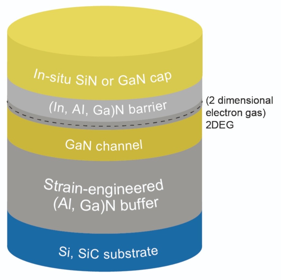
Figure 1. A typical GaN HEMT heterostructure.
When producing GaN HEMTs, an important decision is the choice of substrate. Semi-insulating SiC is selected to meet the need for ultimate power levels in the most demanding applications, while silicon’s strengths are related to low-costs, large diameters and high-volumes.
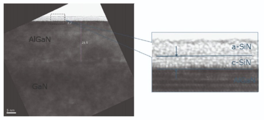
Figure 2. Transmission electron microscopy of an in-situ SiN-capped AlGaN/GaN HEMT structure showing the nature of the SiN. This material is crystalline close to the interface to the barrier, and amorphous when further from it.
At epiwafer supplier EpiGaN, now part of Soitec, we leave it to our customers to decide whether a SiC substrate, or one made from silicon, is the best choice for their RF application. Our focus is to produce the best GaN HEMT heterostructure for a specific application on each of these foundations, through judicious choice of the barrier and the cap layer.
In order for GaN-on-silicon to compete directly with GaN-on-SiC in high-end RF applications, a few technical hurdles have to be overcome. Some of these are intrinsic, including the lower thermal conductivity of silicon compared with SiC – in this case, the solution is an aggressive reduction of the substrate thickness to 50 µm. But there are also other issues, such as the conductive interface that is formed between the silicon substrate and the III-nitride buffer layer during epitaxial deposition. This parasitic conduction path is highly detrimental, as it capacitatively couples to the HEMT channel. It is to blame for the undesired dissipation of RF signals, which increase with frequency. When transistors are manufactured on such lossy substrate/buffer combinations, they fail to deliver good performance at high frequencies, in terms of gain, power and efficiency.
To suppress this undesirable conductive path, we have developed and optimised a robust interface technology. This trims RF signal loss on GaN-on-silicon material to well below 0.4 dB/mm for frequencies up to Ka-band. Such a low loss enables the RF performance of GaN-on-silicon HEMTs to get very close to that of their GaN-on-SiC cousins. Using this process, which can be used on high-resistive silicon substrates up to 200 mm diameter, we have produced epiwafers that are ideal for making devices for the 5G sub-6 GHz and millimetre-wave frequency bands.
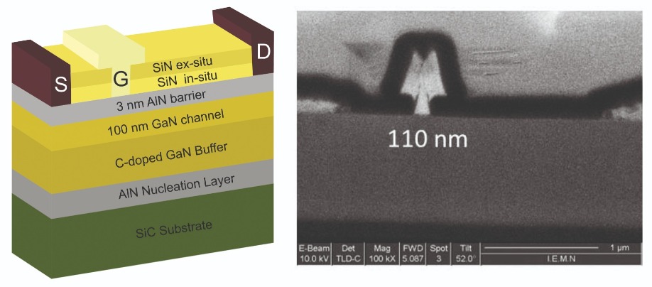
Figure 3. 110 nm gate length GaN-on-SiC HEMT structure using a 3 nm AlN barrier capped with 10 nm in-situ SiN; courtesy of F. Medjdoub, IEMN, Lille.
Today, the workhorse for RF power amplifiers operating in sub-6 GHz bands is a GaN-on-SiC HEMT with a 20 nm-thick AlGaN barrier that has an aluminium content of around 25 percent. This ternary barrier is capped and protected by an ultra-thin GaN layer, typically 2-3 nm thick (see Figure 1).
Our view is that there are times when this mainstream barrier may not be the best choice in more demanding millimetre-wave band and low-voltage applications. For these cases, we have developed heterostructures that combine an in-situ SiN protecting layer with either a binary AlN layer or a lattice-matched InAlN barrier. We will now outline the merits of both these options for the barrier.
One of the strengths of the binary AlN barrier it that it allows a reduction in the thickness of this layer from typical values of around 20 nm to between just 3 nm and 6 nm. This opens the door to bringing the transistor gate very close to the densely populated channel, and in turn maximising the electrostatic coupling between the two – this leads to improved gate control, and ultimately superior RF transistor characteristics.
For example, the transistor’s transconductance increases when the gate is brought closer to the channel. In addition, there is a suppression of short channel parasitic effects, which can impair transconductance when scaling transistor gates below 0.15 µm. Another benefit of the AlN barrier is that it has a very high inherent piezoelectric effect, resulting in carrier densities in excess of 2 x 1013 cm-2 in the transistor’s two-dimensional electron gas. This leads to a hike in power density, and also a significant reduction in chip size, so long as an appropriate thermal chip layout is used.
By turning to InAlN, rather than AlN, it is possible to produce a lattice-matched barrier by using the alloy In0.17Al0.83N. Pairing this ternary with GaN is attracting much attention, because this combination has a large spontaneous polarization, but is not impaired by a high degree of strain, which is found in AlGaN/GaN. These merits enable heterostructures of InAlN/GaN to have significantly higher sheet carrier densities than those of AlGaN/GaN, while maintaining good electron mobility. At the device level, this means that HEMTs have higher maximum current capabilities, a valuable asset for high-power devices operating up to millimetre-wave frequencies.
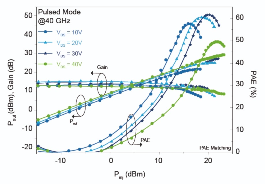
Figure 4. Pulsed power performance at 40 GHz of a 2 x 50 µm AlN/SiN HEMT (gate length 110 nm, gate-to-drain spacing of 1.5 µm) at Vds of 10 V, 20 V, 30 V and 40 V*, *power matching only; courtesy of F. Medjdoub, IEMN, Lille.
On the top of our epiwafers we add a high-quality SiN layer, grown in-situ by MOCVD. As the first few monolayers of the SiN are crystalline, the interface trap density is very low (see Figure 2).
This SiN layer can serve many purposes. It can provide surface passivation, sealing the top of the GaN wafers directly after growth; it can be used as a gate dielectric; it can stop relaxation of the strained barrier layers; and it can prevent exposure of III-N layers to the fab environment, enabling the processing of GaN-on-silicon wafers in silicon CMOS fabs.
Yet another benefit of the in-situ SiN capping layer is that it controls the filling of the surface states during device operation. This can combat current collapse, which is associated with the depletion of the two-dimensional electron gas. Current collapse is avoided because the addition of SiN provides enough charge to neutralize the surface charge of the AlGaN barrier layer, so that its surface potential no longer contributes to the two-dimensional electron gas depletion. Finally, when SiN layers are added to HEMTs, these devices have a superior stability at high temperatures.
Millimetre-wave merits
For devices operating in the 5G millimetre-wave bands, a premium is placed on performance at high frequencies. HEMTs are scrutinised for their gain, power density and power-added efficiency, and this reveals that those that are made from standard AlGaN/GaN heterostructures are not the best choice for Ka-band 5G massive MIMO antenna systems. A better option for these challenging specifications are designs that feature ultra-thin AlN or lattice-matched InAlN barriers in combination with in-situ SiN cap layers. HEMTs with these hallmarks deliver excellent performance, by suppressing short-channel effects while simultaneously realising the highest current densities.
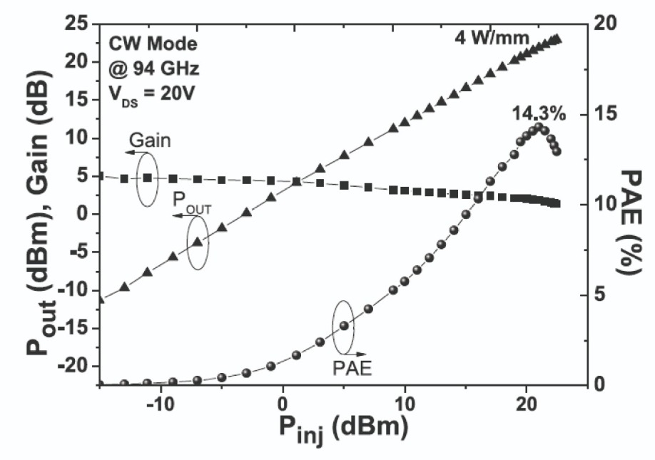
Figure 5. Continuous-wave power performance at 94 GHz of a 2 x 25 µm AlN/SiN HEMT (gate length 110 nm, gate-to-drain spacing of 0.5 µm) at Vds=20V; courtesy of F. Medjdoub, IEMN, Lille.
We have also collaborated with Ommic, a leading 150 mm European GaN foundry, to provide further proof of the performance of devices produced with our material. Ommic has developed a 100 nm gate-length, open foundry MMIC process with a complete design kit on our SiN/AlN/GaN-on-silicon HEMT technology.
The devices produced in the Ommic line provide further verification of the superiority of GaN HEMTs made with our material over standard GaAs pHEMT processes. The breakdown voltage is much higher, hitting 40 V, and this leads to a much higher Ka-band output power density – it is 3.5 W/mm at 30 GHz – alongside a higher robustness to input mismatch conditions.
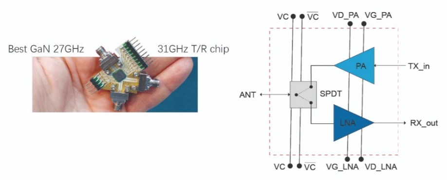
Figure 6. Fully integrated millimetre-wave 5G 26-34 GHz transmitter/receiver product utilising EpiGaN’s GaN-on-silicon RF HEMT epiwafer technology; courtesy of Ommic, Limeil Brévannes, France.
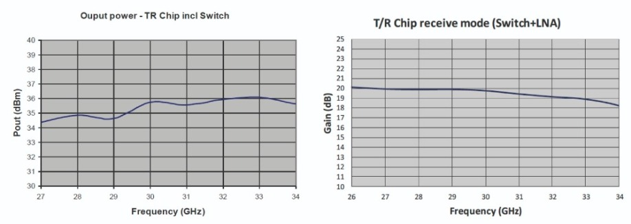
Figure 7. Transmitter power amplifier output power and receiver small-signal gain of a millimetre-wave 5G GaN-on-silicon transceiver MMIC shown in Figure 6; courtesy of Ommic, Limeil Brévannes, France.
At the same time, GaN-on-silicon is quickly closing the performance gap, while offering an attractive opportunity to drive down costs through economies of scale. This is helping RF GaN technology to start to enable innovations in many existing applications.
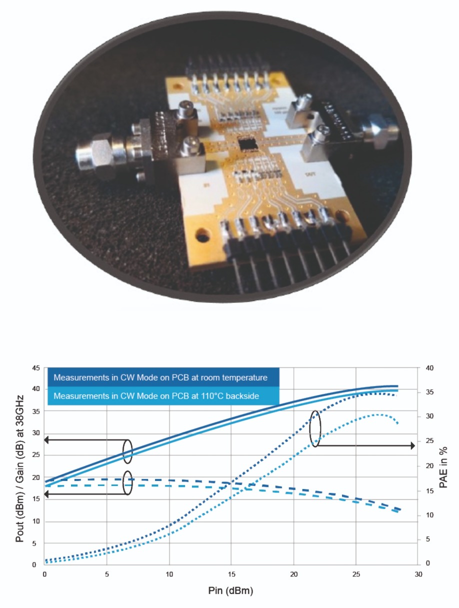
Figure 8: Output power, gain and power-added efficiency of a 5G 40 GHz GaN-on-silicon power amplifier; courtesy of Ommic, Limeil Brévannes, France.
What about the smartphone, now the holy grail for every semiconductor technology? At first glance GaN is not ideal, as the higher supply voltages – typically 10 V or more – are not well suited to handsets, which typically use between 3 V and 5 V. But that’s not a show-stopper as this gap can be bridged with device process adaptations. Some of the biggest component suppliers in the handset business are already discussing GaN-on-silicon for 5G millimetre-wave enabled smartphones.
Standards will continue to evolve, due to the introduction of carrier aggregation and the ever increasing performance requirements for multi-mode, multi-band power amplifiers. This may play into the hands of RF GaN-on-silicon technology, which offers the inherent benefits of scaling, and could soon become a strong contender for 5G mobile devices.

Techniques for supressing degradation in SiC p-i-n diodes and IGBTs, enhancing channel mobility in SiC MOSFETs, and improving the blocking voltage and on-resistance of Ga2O3 transistors were all unveiled at the most recent IEDM meeting.
BY RICHARD STEVENSON
TURN ON THE NEWS and there’s a good chance you’ll hear a story related to climate change. Recently the focus has been on the devastating fires in Australia, but in the last few months you may also have read of accelerated ice-melting in Greenland, demolition of homes in Rwanda to protect citizens from flooding, and the breaking of global temperature records.
For those of us that see climate change as man-made, our challenge is to modify our lifestyle, so that we help to curb carbon emissions. Some of the changes that we could consider may not be to our liking, such as switching to a more plant-based diet and taking fewer flights to sunny climes. But there is one change that we will applaud: far greater deployment of more-efficient power electronics, based on devices made from alternatives to silicon.
Leading this charge is SiC. Sales of diodes and transistors made from this material are ramping fast, as the uptake of these devices branches out from their deployment in power supplies and inverters to electric vehicles, where they enable an extension to the driving range. Far behind, but with even greater promise, is gallium oxide, a material with an even wider bandgap. It will not be long before the first commercial Ga2O3 devices appear on the market, but significant sales are still some years away.
For both SiC and Ga2O3, long-term success hinges on making the devices better and better. Performance must improve, alongside reliability. To succeed, more research is needed to understand the behaviour of the diodes and transistors, and how modifications to designs impact device behaviour.
Presentations detailing progress of this nature were detailed at the latest International Electron Devices Meeting (IEDM). Held in San Francisco between 7 and 11 of December, researchers at IEDM 2019 described techniques to suppress bipolar degradation in SiC p-i-n diodes and IGBTs, improve the characteristics of the channel in SiC MOSFETs, and a Ga2O3 transistor architecture that sets a new benchmark for breakdown voltage.
Supressing bipolar degradation
Sales of SiC power devices are dominated by Schottky barrier diodes and MOSFETs. Within this commercial product portfolio there are devices designed to operate between 600 V and 3.3 kV. Higher voltages are possible, but for values of 10 kV and above, SiC p-i-n diodes and IGBTs appear to be better alternatives. However, if this pair of devices are to fulfil their potential, a condition known as bipolar degradation must be addressed. This degradation occurs when current passes through these devices and stacking faults arise, leading to an increase in forward voltage. Note that a solution to this impediment could have wider implications, as this type of affliction may also occur in body p-n diodes of SiC MOSFETs.
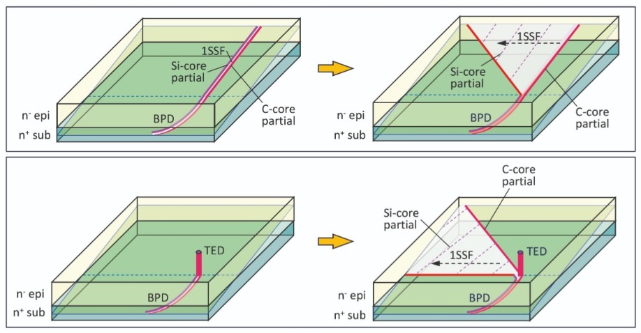
Figure 1. Basal plane dislocations (BPDs) in the substrate can propagate into the epilayer (top left), or be converted into threading edge dislocations (TEDs). Most of the BPDs in the epilayer contain a pair of partial dislocations – one with a silicon core, and the other with a carbon core – with a single Shockley stacking fault (1SSFs) between them. Once the carrier density exceeds a threshold, there is an expansion of 1SSFs from the BPDs in the epilayers to create a right-angled triangular 1SSF (top right). This expansion forms across the current pass of the device, leading to an increase in forward voltage. There can also be an expansion of 1SSFs, involving bar-shaped 1SSFs to expand from the BPD segment below the BPD-TED conversion point (bottom right). This can be caused by the injection of minority carriers into a region below the BPD-TED conversion points located near the epilayer and substrate interface, and also in substrates with a high density of BPDs.
When basal plane dislocations are in the epilayers, once the carrier density exceeds a threshold, there is an expansion of single Shockley stacking faults (see Figure 1). Eventually, right-angled triangular single Shockley stacking faults are formed across the current pass of the device, leading to an increase in forward voltage.
At IEDM several approaches to combat bipolar degradation were described by Hidekazu Tsuchida from Japan’s Central Research Institute of Electric Power Industry (CRIEPI).
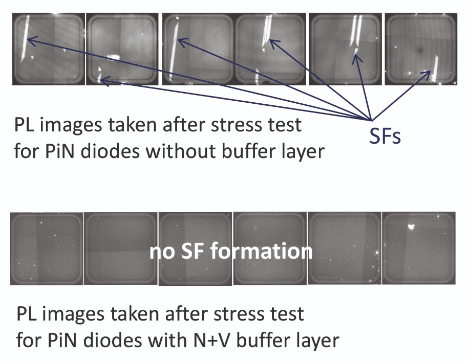
Figure 2. Photoluminescence measurements on p-i-n diodes that have been subjected to a stress test show that the addition of a buffer layer (bottom set of devices) eradicates the formation of single Shockley stacking faults.
Back in 2018, Tsuchida and co-workers reported a study involving the fabrication of SiC p-i-n diodes. This effort involved using electroluminescence to determine the threshold current associated with the expansion of single Shockley stacking faults. By measuring the charge in the drift layer during turn off, the researchers converted the current density to a hole density. This revealed that the threshold for the hole density in an n-type layer is 1-2 x 1015 cm-3.
Based on this insight, Tsuchida and co-workers argue that two criteria must be met to ensure the suppression of bipolar degradation. They are the elimination of basal plane dislocations from the region where minority carriers are injected, and the reduction in the minority carrier density to a level below threshold in the region where basal plane dislocations exist.
According to Tsuchida, both these requirements are needed because even if basal plane dislocations in the substrate are perfectly converted to threading edge dislocations at the interface between the epilayer and the substrate, minority carriers are still injected into the substrate. Here, the danger is that the density of these carriers exceeds the local threshold, triggering conversion of the basal plane dislocations in the substrate into stacking faults.
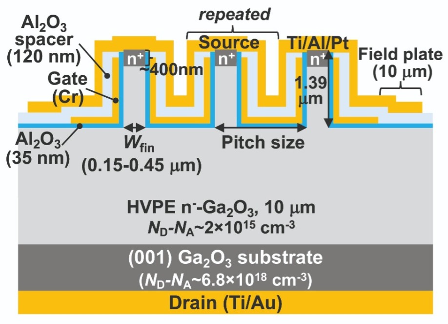
Figure 3. Ga2O3 transistors with multiple fins have broken the record for the blocking voltage for this class of transistor. A portfolio of devices has been produced, with fin channel widths ranging from 0.15 µm to 0.45 µm, and pitch sizes from 1.2 µm to 2 µm.
Initially, the team turned to nitrogen doping to reduce the carrier lifetime in the buffer. However, when the nitrogen concentration exceeded 1-2 x 1019 cm-3, this introduced an imperfection known as a double Shockley stacking fault. Keeping the nitrogen concentration low enough to avoid this shortened the carrier lifetime to around 40 ns.
To further reduce this lifetime, Tsuchida and co-workers have recently switched to doping with vanadium, a deeper dopant. When present at a concentration of just 7 x 1014 cm-3, room-temperature carrier lifetime is shortened to just 13 ns.
The benefit of vanadium doping has been assessed by comparing two sets of SiC p-i-n diodes. Controls features a 10 µm-thick, nitrogen-doped drift layer grown on an n-type substrate, and modified variants have an additional buffer, doped with vanadium and nitrogen, inserted between the substrate and drift layer.
To evaluate the impact of the buffer, measurements were made on 16 controls and 16 variants. Initial forward voltages, recorded at a 18 A drive current, were compared with values after one stress test and then another. The first involved driving diodes at 300 A cm-2 for an hour, and for the second, devices were run at 600 A cm-2 for an hour. Analysis of the results showed that the buffer layer leads to a substantial reduction in variation of forward voltage after operation.
Further insight into the difference between standard devices and those with a doped buffer has come from photoluminescence measurements. This optical technique exposed single Shockley stacking faults in the conventional diode, and the absence of these faults in the modified design (see Figure 2).
Buffer layers may also benefit SiC IGBTs. This type of device would require a p-type buffer layer with a short carrier lifetime. Aluminium, which forms a shallow acceptor, is a candidate for doping, as increases in its concentration reduce carrier lifetime. Tsuchida and co-workers suggest that this might be combined with boron, which greatly shortens carrier lifetime.
One of the goals for the team is to map, with precision, the locations across a wafer where basal plane dislocations are converted into threading edge dislocations. Such a study promises to enable a more detailed, quantitative understanding of the expansion of single Shockley stacking faults, and could also aid the development of drift and buffer layers that improve the performance of bipolar devices.
Another target for the researchers is the development of a fast growth technique for making 4H SiC that will trim the density of basal plane dislocations and threading dislocations. The team have already made much progress, realising a growth rate of 3 µm/hour. “[That’s] about ten times higher than a typical PVT growth,” says Tsuchida.
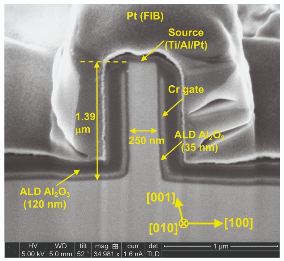
Figure 4. A scanning electron microscopy image of the fins in the Ga2O3 transistors highlight the near-vertical sidewall profile produced by dry etching.
The introduction of a new dopant is also behind the improvements made to the performance of SiC MOSFETs. This success, realised by a team from Mitsubishi, involved the introduction of oxygen doping. It led to a significant reduction in channel resistance and an increase in the threshold voltage.
Both of these attributes are highly desired by the designers of power electric systems. Reducing resistance cuts energy losses, and a higher threshold voltage makes it easier to control the system.
Normally these improvements are realised by nitridation. However, if the threshold voltage exceeds 3 V, this comes at the expense of a hike in channel resistance.
The team from Mitsubishi have previously addressed this weakness by switching to sulphur. And at IEDM they revealed the results of using another alterative, oxygen, which is a far deeper donor. Spokesman for the team, Munetaka Noguchi, claims that there are no downsides to the use of deep donors. He arrived at this conclusion after considering the results of pulsed measurements that enable an estimate of threshold voltage stability.
Noguchi and co-workers have produced vertical and lateral SiC MOSFETs with oxygen doping. For commercial sales, vertical MOSFETs are preferred. “We used lateral MOSFETs as a test structure to evaluate channel performance,” explains Noguchi.
Ion implantation provided a relatively high concentration of oxygen near the channel. Note that such a high concentration is not possible with simple thermal oxidation. Following thermal activation of oxygen, the team formed the gate oxide with thermal oxidation and nitridation in dilute nitrogen oxide.
Measurements of the capacitance of the MOS capacitors in the lateral MOSFETs revealed that at elevated temperatures the introduction of oxygen increases capacitance in the depletion region. This work also revealed that oxygen acts as a donor, rather than an acceptor-like trap.
Additional benefits of the introduction of oxygen in lateral SiC MOSFETs include a 46 percent reduction in channel resistance, realised for a threshold voltage of 3.9 V.
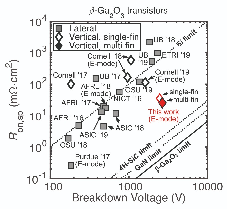
Figure 5. Multi-fin Ga2O3 transistors produce by a partnership between researchers at Cornell University and Hosei University have broken the record for blocking voltage for this class of device. Note that the on-resistance is normalised using an effective conduction width of about 10 mm, as normalising this resistance to the source contact area would grossly over-estimate the figure of merit.
When using any deep level donor, there is an increase in the threshold voltage drift at elevated temperatures. “However, the magnitude is suppressed in the oxygen doped sample,” says Noguchi. Compared to sulphur, this shift is almost halved.
Another benefit of using oxygen rather than sulphur is that it produces a smaller shift in negative bias temperature instability. This indicates that the reliability of the gate is better – it is, in fact, comparable to that in a conventional device.
Noguchi and co-workers will continue to investigate the impact of deep level donors on the electrical characteristics of the MOSFET. In particular, they will consider its ruggedness as a power switching device.
Another option for decreasing the resistance of a SiC MOSFET is to use a trench architecture. This design also allows a smaller cell pitch, leading to an increase in channel width.
However, the trench MOSFETs that have been fabricated on commercial SiC (0001) substrates are failing to fulfil their promise. The field-effect channel mobility is lower than that expected for planar MOSFETs, for reason that are not clear.
To shed light on this matter, a team from Toyota Central R&D Labs has tried to determine the mobility in the channel. To extract an accurate channel resistance, they remove parasitic series resistance from their calculations.
According to the researchers, the key to calculating the field-effect channel mobility is to determine the threshold voltage. Due to the high density of charge traps at the interfaces of SiO2 and SiC, there are inaccuracies associated with calculations of threshold voltage that are based on linear extraction. To avoid this, the team determines the threshold voltage by drawing on values of the ideal threshold voltage and experimental measurements of the relationship between the drain current and the gate voltage.
The first step towards this involved growing n-type and p-type epilayers of SiC on a heavily doped n-type SiC substrate. After adding source and drain regions, the researchers fabricated a trench gate. Following trench etching, they used three different forms of high-temperature annealing to produce different surface morphologies in the trench walls. To complete the fabrication of the structure, they added a 75 nm-thick layer of SiO2, followed by nitridation of the device in diluted nitrogen oxide.
Plotting the drain current as a function of gate voltage at a range of temperatures enabled the team to calculate the density of fixed charges and the distribution of interface states. From these values, the researchers concluded that the interface states contribute to Coulomb scattering.
To relate the level of scattering to the quality of the channel, the team scrutinised the surface morphology of the trench sidewalls with atomic force microscopy. This revealed a significant difference in the roughness of the three samples. By combining this finding with the electrical measurements, they deduced that Coulomb scattering is suppressed when the trench sidewalls are flat enough to form atomic steps and terraces. In this case channel mobility is higher, due to a decrease in the distribution of interface states that arises from dangling bonds at the edge of the step region.
Record-breaking voltages
Helping to improve the performance of Ga2O3 transistors is a partnership between researchers at Cornell University and Hosei University. This team has broken the record for blocking voltage with a vertical transistor that can withstand 2.66 kV. This raises the bar from 2.32 kV, a figure obtained with a lateral variant.
Team spokesman Wenshen Li from Cornell University says that one of the merits of the vertical architecture, which leads to vertical current flow, is a more efficient use of the device footprint. “[Devices] typically have a smaller area, especially under high current ratings.”
By using a sub-micron fin-channel structure for the device architecture (see Figure 3), Li and co-workers avoid the need for p-doping. That’s a significant advantage as p-doping in Ga2O3 is impaired by: deep acceptor levels that hamper the thermal activation of these carriers; a very flat valence band, which leads to a high effective mass for holes and impairs conductivity; and self-trapping of holes.
One of the reasons why Ga2O3 transistors are failing to fulfil their potential is that the channel mobility is far lower than it is in the bulk, due to etch damage and sidewall depletion. Effective channel mobility is typically just 30 cm2 V-1 s-1, compared to values of up to 200 cm2 V-1 s-1 for bulk material.
To address this, Li and co-workers use a post-deposition annealing step during the production of their transistors. Some of these devices contain several fins, enabling unambiguous evaluation of the specific on-resistance – it breaks new ground for Ga2O3 transistors.
Fabrication of the team’s devices began by loading an n-type Ga2O3 substrate into a HVPE chamber and depositing a 10 µm-thick, lightly doped n-type drift layer. Silicon implantation and subsequent activation at 1000 °C created a heavily doped n-type top layer that provided an ohmic contact. Electron-beam lithography defined the fins (see Figure 4), which were formed by dry etching.
After treatment with HF to remove plasma damage, the team added a Ti/Au drain contact and a gate contact, comprising a 35 nm-thick Al2O3 gate dielectric created by atomic layer deposition and a 50 nm-thick layer of chromium, deposited by sputtering.
During the formation of the source electrode of Ti/Al/Pt by sputtering, Li and co-workers simultaneously created a source-connected field plate. This refinement to the design provided a significant improvement to edge termination, and is behind the increase in breakdown voltage.
“However, we found that the breakdown voltage is still limited by the edge termination, indicating that the source-connected field plate is not an optimal design,” admits Li.
The team have used electrical measurements to evaluate the benefit of post-deposition annealing. It leads to a significant increase in current density, an improved source contact resistance, and a reduction in interface trapped charges, leading to a lowering of the sidewall depletion in the fin channels.
Using simulations and fits to experimental data, channel mobility in single-fin devices is found to be around 130 cm2 V-1 s-1. This figure drops to just 40 cm2 V-1 s-1 in multi-fin devices, due to rougher sidewalls that result from plasma loading effects during the dry-etching step. “By tweaking the plasma condition during the dry etching for a more anisotropic etch, the roughness can be reduced,” say Li.
The multi-fin device outperforms its single-fin variant in blocking voltage, realising a value of 2.655 kV, compared with 2.46 kV. Additional measurements on the multi-fin transistor reveal an on-off ratio in excess of 108; a threshold voltage of 1.8 V at 0.1 mA cm-2; and a specific on-resistance of 23.2 mΩcm2, based on pulsed-measurements that are expected to reduce self-heating and charge trapping (see Figure 5 for benchmarking of the single-fin and multi-fin devices) .
Plans for further work include optimising the dry etching process, in order to improve channel mobility in multi-fin channel devices, and developing better edge termination designs for improved breakdown behaviour. Li says that additional goals are to undertake thermal characterisation of their devices, and the testing and analysis of dynamic behaviours.
The presentations at IEDM by Li on Ga2O3 transistors, and by other speakers on SiC devices, show that power electronic devices are getting better. That bodes well for the future, where greater deployment of more efficient power electronics is set to play its part in global efforts to tackle climate change.
Increasing the size of the waveguide on a photonic integrated circuit significantly reduces optical loss, boosts power handling and enables efficient coupling to the laser.
BY AARON ZILKIE AND GREG FINN FROM ROCKLEY PHOTONICS
Silicon photonics holds the key to bringing photonic integrated circuits (PICs) to many more applications. PICs that sport silicon photonics promise to: increase the bandwidth and the power efficiency in data centres; provide low-cost, solid-state technologies for LiDAR operating at eye-safe wavelengths; deliver advanced computing solutions; and transform network communications, sensing and 3D imaging.
Today, the majority of silicon photonics players are focusing their efforts on developing monolithic products, which integrate photonics structures with CMOS on a single semiconductor chip. At first glance this is an attractive approach. However, if you delve more deeply drawbacks appear. One of the biggest of these is that due to physical and economic considerations, CMOS silicon photonics is not going to fulfil its full potential and scale. Why? While the scaling of CMOS technologies delivers benefits to the performance of electrical circuits, success is not replicated with photonics. Instead, multiple issues arise, because key photonics structures struggle at sub-micron dimensions. There is also another major issue – the materials available within a traditional CMOS semiconductor process cannot support the implementation of every electro-optic structure. Take, for example, the laser, which requires the processing of III-V materials.
The technology that we have developed at Rockley Photonics takes into account all these issues. Our approach is to begin with a clean sheet – a completely different process flow, unconstrained by the limitations of legacy CMOS processes that have been optimised for VLSI electronic devices.
From this starting point, we have been developing and optimising a proprietary photonics manufacturing technology since our foundation in 2013. We are able to draw on a depth of expertise that goes back some thirty years, and is aided by our close working relationship with our foundry partners. The platform that we are pioneering has great versatility, offers broad applicability across many product applications and markets, and enables high-volume production.
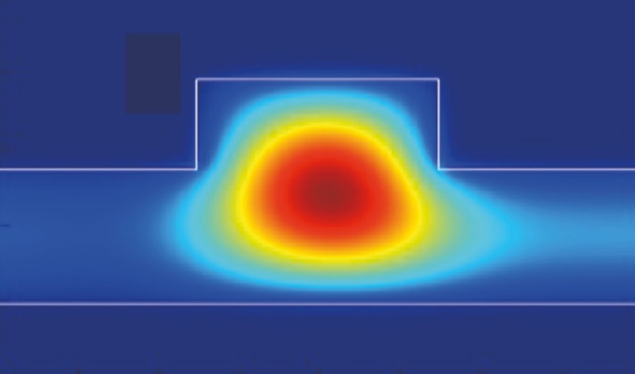
Simulation shows excellent confinement for single-mode light propagation in Rockley Photonics’ 3 µm-high waveguides. This single-mode propagation is maintained even if the waveguide is excited off-centre.
At the heart of our technology is the use of larger, multi-micron waveguides, which hold the key to optimising PIC performance, power efficiency, manufacturability and versatility. Compared to a conventional architecture, our platform has: up to ten times lower waveguide loss; a 25-fold reduction in performance variability, due to changes in waveguide dimensions; polarization independence; and a low-loss, monolithic, ultra-broadband fibre attach technology.
By reducing propagation loss, our multi-micron waveguides enable PICs to serve the widest possible range of applications. We tackle the leading contributor to propagation losses, electromagnetic field scattering, which is caused by roughness in the sidewalls of the waveguide. Reducing this roughness is far from easy – a simpler approach is to minimise the transmitted light’s modal overlap with the side walls. This is what we do with our multi-micron waveguides, to make them outperform their conventional sub-micron equivalents. Our waveguides combine improved confinement with a reduction in modal overlap with waveguide side walls – factors that also enable high integration capabilities.
In many applications, it is important for a PIC to have a high power-handling capacity. For example, with LiDAR, high output powers enable the generation of images at extended ranges and high frame rates – leading to the delivery of more photons on target down range. With silicon photonic chips, power-handling capacity is limited by a saturation effect associated with the simultaneous absorption of two photons. This absorption loss is governed by the spatial intensity of the light in the waveguide, so is substantially different in sub-micron and multi-micron waveguides. In 3 µm waveguides, power can be 30 times higher than it is in 220 nm waveguides before there is a 1 dB power loss due to two-photon absorption.
Another valuable attribute for 3 µm waveguides is that they support single-mode operation, which minimises dispersion and signal degradation. It may come as a surprise to some that our multi-micron waveguides are capable of this – and they do so while offering several advantages over a conventional sub-micron variant, including simultaneous realisation of low-loss coupling to standard single-mode fibre and III-V active devices, very low propagation losses, high tolerance to fabrication variations and polarization independence. The latter is realised by setting the waveguide rib width-to-height ratio close to unity, and ensuring that the transverse electric and transverse magnetic modes have similar values for the effective index. We produce PICs that have all these attributes and a range of waveguide sizes with cross-sectional dimensions from 1 µm to 13 µm.
An additional merit of multi-micron waveguides is that they can realise tight bends. This is highly valued – designers want to produce high-density photonic circuits, so they are keen to avoid large bends that hinder compact PIC designs, waste valuable silicon space and result in larger chip and package sizes. Our multi-micron waveguides are ideal, as they can have tight bends while avoiding losses and mode leakage, because they provide strong confinement of the electromagnetic wave. To do this, we convert the rib waveguides into strip or wire waveguides in the parts of the circuit where tight bends are needed, and employ a special design known as an Euler bend in the high-confining strip waveguide.

Bends in Rockley’s 3 µm waveguides.
We have shown through simulation and measurement that our multi-micron waveguides produce a far lower phase error and wavelength variation than sub-micron counterparts. For a 3 µm waveguide, the variation in effective refractive index is 20 to 40 times lower than it is in 220 nm waveguides.
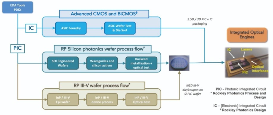
Rockley Photonics manufacturing flow.
In addition to developing multi-micron waveguides, we have created a portfolio of key building blocks. They include lasers, modulators, photodetectors and filters, all of which utilise the attributes of the platform.
To add a laser to our PIC, we have to integrate a III-V semiconductor device, because silicon is a poor light emitter. This addition is relatively easy for us, because laser diodes naturally also have a multi-micron mode size.
We attach the fully processed lasers directly, in a recess that we etch into the silicon waveguide. This facilitates edge coupling, which enables low-loss and dense laser integration to produce PICs with a compact form factor, while still realising high manufacturing tolerances. This approach is also highly versatile, enabling us to integrate a wide range of lasers – different materials and designs – using a flip-chip die bonding approach.
The lasers that we add have excellent characteristics. They have very narrow linewidths and output powers that can exceed 50 mW at room temperature. Those with a hybrid distributed feedback design are tolerant to back-reflections, having up to -20 dB return loss at the laser facet. This is a very valuable attribute, as commercial lasers used in silicon photonics have to operate in the presence of multiple sources of scattering and back reflection.
Our platform is also ideal for ultra-broadband applications. It can produce many-channel laser PICs, built by harnessing multi-cavity and multi-material wafer-scale integration techniques.
We have also developed processes for adding electro-absorption modulators and photodetectors to our chips. These devices are critical components in products across multiple markets including optical fibre and datacentre communication transceivers.
A well-diversified toolbox enables platform versatility.
Germanium photodetectors, which convert light signals back to electric signals, are also made in this platform with excellent performance. These polarization-independent, broadband devices have electro-optic detection bandwidths of over 40 GHz, sufficient for detection of 50 Gbit/s NRZ and 100 Gbit/s PAM-4 signals.
Filters are an essential ingredient in PICs, performing functions that include wavelength-division multiplexing, a technology that enables high-bandwidth data transfer. The most common way to realise this is to use arrayed waveguide gratings. This form of filter is far better with multi-micron waveguides than sub-micron variants, because the larger dimensions lead to a lower birefringence, polarization independence, and a reduction in phase errors and propagation losses. Thanks to these attributes, arrayed waveguide gratings, produced in our platform, provide high performance and repeatability. By incorporating Euler bends into these arrayed waveguide gratings, they are far more compact, opening the door to their integration into high-density PICs.
One of the downsides of forming PICs with silicon is that this material has a high thermo-optic coefficient, which hampers heat management. To address this, we deploy heaters that deliver around a 1 mW/p phase change – they can be positioned within waveguides to manage thermal energy. In addition, with just a few additional processing steps, our arrayed waveguide gratings made with only silicon can be made temperature independent. These gratings produce almost no drift in wavelength due to temperature variation.
For many applications, optical signals need to be transferred from the chip to the fibre. This requires an interface between PIC waveguides and single-mode optical fibre. If the PICs are to be competitive in high-volume products, this attachment should be low-cost, low-loss and simple to align.
We tick all those boxes, thanks to the use of a mode size that is in the same ballpark as that of single-mode fibre. A single-stage spot size converter enables us to mode-match between 3 µm waveguides and 13 µm waveguides, and then directly couple to single-mode fibre. Etching V-grooves into the silicon allows us to accurately align the single-mode fibre to 13 µm waveguides and also hold the fibre in place, creating the most simple and elegant fibre attach solution for photonic integrated circuits.

Rockley’s platform serves multiple sectors from communications to sensing
The strengths of our platform are not limited to its performance, but extend to its suitability for broad applicability, high-volume manufacturing and large-scale deployment. These advantages are partly due to a production process that realises high yields, thanks to low device sensitivity to process variations. However, there are additional merits of our technology. It is capable of integrating a large number of components at a high density; it produces low optical loss interfaces; and III-V materials are integrated in an efficient manner. What’s more, data throughput densities can exceed 200 Gbit/s/mm, due to our high-speed, compact, low-power modulator and detector technologies and interface electronics; and fibre coupling losses can be less than 1 dB with our simple, high-yield, high-throughput fibre attach assembly.
Using a complex manufacturing flow that involves many partners, we have also developed and implemented analogue, digital and mixed-signal electronics design and integration. This has enabled us to ship complete photonic chips and chipsets to serve different market sectors.
Ideally, silicon photonic chips form part of a set of wider technologies, together with CMOS, BiCMOS and packaging. We are able to incorporate all of these in a complete chipset, making our multi-micron silicon PIC platform a strong candidate in many markets.
One of these markets is data communications, where there is a rising global appetite for data-centre bandwidth. This is driving demand for in-package optics which involves integrating fibre-optic links with ICs. To enable edge integration, these ICs require high-bandwidth, compact PICs operating at more than 200 Gb/s/mm, a specification we can satisfy.
In addition, there is a need to keep pace with increasing bandwidth capabilities of switch ASICs, by scaling PIC modulators and detectors to higher data rates, while increasing their integration density. Our modulators and detectors are ideal for this task. Using our platform, transceiver PICs are smaller than 30 mm2 – that is comparable to, or smaller than, those made using sub-micron photonic platforms.
With an optical power handling capability of over 2 W, our multi-micron platform is also well suited to sensing applications, such as 3D imaging and LiDAR. These applications can involve the transmission of large optical powers, and require fast, steerable, narrow beams for high resolutions at high frame rates. One strength of our platform is its demonstrated capability to implement coherent receivers, an essential ingredient for frequency-modulated continuous wave LiDAR. This advanced form of LiDAR collects 3D imaging and velocity measurements – data that is much sought after by those developing advanced driver-assistance systems and related autonomous technologies for the automotive and transport markets.
Another strength of our platform is its high light confinement. This allows many emitters to fit on a tight pitch, aiding design of optical phased arrays, which can provide fast steering when equipped with waveguide diodes with response times of 10 ns or less.
Using our technology, we have demonstrated a high level of integration with many photonic devices including: compact arrayed waveguide grating filters, hybrid lasers, and high-speed modulators and detectors. Our platform’s versatility, combined with the physical benefits it brings, enables our technology to target many applications, from data communications to sensing. Competitiveness in these sectors is assured, because we are able to leverage a key success factor that microelectronics also enjoyed: the ability to deliver economies of scale with high-volume manufacturing made possible by multi-market technology applicability.
Wafer bonding opens the door to the fabrication of multi-colour, high-resolution imagers.
BY Sanghyeon Kim, Dae-Myeong Geum FROM Korea Advanced Institute of Science and Technology, Won Jun Choi FROM Korea Institute of Science and Technology AND Euijoon Yoon FROM Seoul National University
Deployment of photodetectors is on the rise. Those operating in the visible are now a key feature in smartphones, and variants detecting in the infrared are being used in surveillance and the development of autonomous cars.
Product designers are selecting photodetectors that operate within a particular spectral domain to retrieve specific information. Detectors of visible light provide visual information our eye can see. Meanwhile, those operating in the infrared, where our eyes cannot see, offer details of the height of an object, or some chemical information – this is crucial in many applications.
Recently, there has been great interest in simultaneous detection across different spectral regions. The development of multi-wavelength photodetectors promises to revolutionise sensing and imaging applications, such as gas detection, medical diagnostics, industrial surveillance and time-of-flight sensors. By constructing overlapping images at different wavelengths, it is possible to generate more informative, more accurate, and more creative information.
Downsides of multi-colour photodetectors, including those that have been recently reported and those that have been commercialised, are bulkiness and use that is restricted to the lab. The only approach to making them that has been commercialised is packaging-based integration. This involves the positioning, in a vertical plane, of a silicon photodetector for the visible and an InGaAs variant for the infrared. With this geometry, when light is separated by a diffraction grating, the differing spectral domains are directed at appropriate detectors (see Figure 1). However, adopting this approach hampers the production of compact, high-resolution imaging devices – the detectors are relatively large, and alignment accuracy is limited by the mechanical alignment between the silicon and InGaAs photodetectors.
One alternative is epitaxy-based integration. With this approach, multi-colour photodetectors are formed by growing multiple active regions. This addresses the issue of bulkiness, but due to lattice mismatches between the different sections, the photodetector is impaired by high power consumption and degraded material quality.
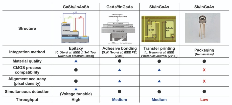
Figure 1. There are many different methods to fabricate multi-colour photodetectors.
A far better way forward, pursued by our partnership between researchers at Korea Advanced Institute of Science and Technology (KAIST), the Korea Institute of Science and Technology (KIST), and Seoul National University (SNU), is the monolithic integration of visible and infrared photodetectors. Employing wafer bonding and epitaxial lift-off techniques, this enables high-resolution, multi-colour imaging.
Multi-colour capabilities
At the heart of our fabrication process is the wafer bonding technique. This low-temperature, low defective process allows us to unite different materials without having to address concerns relating to lattice mismatch (see Figure 2).
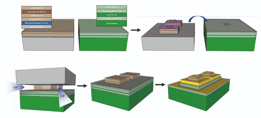
Figure 2. Process flow for multi-colour photodetectors made from GaAs and InGaAs using wafer bonding and an epitaxial lift-off process.
After growing both types of epiwafer, we deposit a layer of Y2O3 on both of them. This oxide is inserted because it is a suitable bonding material, and it has good material stability in the presence of HF, an acid used in the epitaxial lift-off process. After this, we undertake mesa isolation to enhance the speed of the epitaxial lift-off process (this process is detailed in our previous article, published in the June 2017 edition of Compound Semiconductor magazine). The two samples are then bonded together, and the resultant entity dipped in HF acid to separate the GaAs donor substrate from the stack of materials that contains the GaAs photodector, the InGaAs photodetector and the InP substrate. Finally, using standard semiconductor process technology, we undertake metal formation and mesa isolation.
Note that with our approach we form pixels after wafer bonding, using photolithography and etching. This allows us to use a small pitch, and create a high-resolution photodetector (see Figure 3 for microscopic top-view images of fabricated pixels). One of the merits of the multiple pixel array, formed by vertically stacking two photodetectors, is that it delivers twice the resolution of a conventional approach.
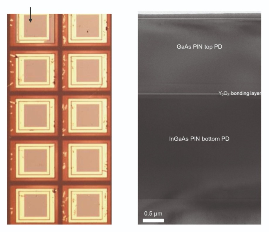
Figure 3. Photographic top-view image and cross-sectional transmission electron microscopy images of the fabricated stacked GaAs visible photodetector and infrared InGaAs photodetectors. These images reveal the good bonding, and also the high material quality after the bonding.
Optical performance
We have broken new ground by demonstrating vertically well-aligned, multi-colour photodetectors formed from typical semiconductor processes. They detect from 400 nm to 1650 nm, a range so broad that it cannot be realised with a single absorbing material (see Figure 4). Measurements of photoresponsivity show similar levels for GaAs and InGaAs photodetectors, highlighting the excellent match between this pair of materials.
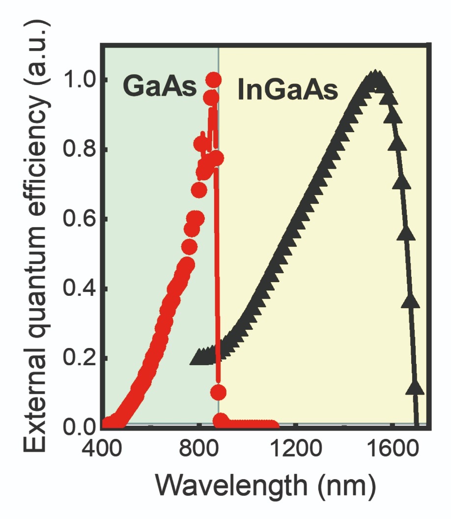
Figure 4. The external quantum efficiency of the fabricated multi-colour photodetectors, highlighting very broad band absorption from 400 nm to 1650 nm.
Our next goal, the fabrication of imagers, requires the hybrid integration of photodetectors with readout integrated circuits (ROICs).
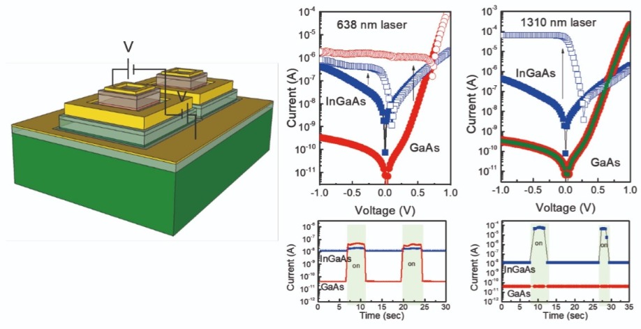
Figure 5. An illustration of the stacked multi-colour photodetectors, and plots of the photoresponse of photodetectors to visible and infrared excitation
We are pursuing a slightly different approach to integrating multi-colour imagers on ROICs. After forming the ROICs, our intention is to bond the first absorbing materials and then the second absorbing materials, processing them using mesa formation, metallization and so on. With this approach, we can draw on the benefits of lithography, which delivers the very precise alignment needed to form high resolution pixels.
Our efforts have enabled us to make great progress towards the fabrication of multi-colour photodetectors. Combining light absorbing layers of GaAs and InGaAs by wafer bonding offers many advantages over conventional integration methods, including good material quality, CMOS process compatibility, precise alignment accuracy between pixels, and simultaneous broad band detection.
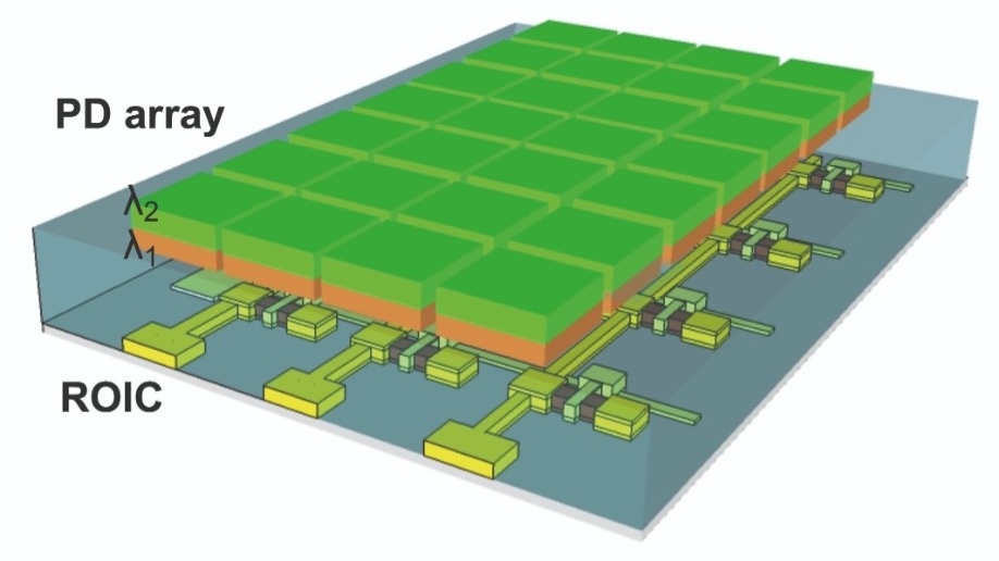
Figure 6. A potential integration method for making multi-colour photodetectors on ROICs.
D. -M. Geum et al., “Monolithic integration of GaAs//InGaAs photodetectors for multicolor detection”, VLSI symposia, p. T248 (2019)
S. Kim et al. Appl. Phys. Lett. 110 153505 (2017)
Designers of blue and green LEDs avoid wide quantum wells, arguing that they impair efficiency, due to built-in fields that pull electrons and holes apart. But that’s an incomplete picture: turn to excited states and high radiative efficiencies are realised over a broad spectral range.
BY GREG MUZIOL FROM THE INSTITUTEOF HIGH PRESSURE PHYSICS, Polish Academy of Sciences
LEDs are everywhere. They are lighting our homes, offices and neighbourhoods; they are backlighting our TVs, tablets and smartphones; and they are in our torches, headlights and many of our gadgets. Sales of these devices now net billions and billions of dollars every year, with success driven by the high internal quantum efficiency of these emitters – in state-of-the-art blue and violet LEDs, the internal quantum efficiency peaks at more than 90 percent.
However, the internal quantum efficiency is not always that high, due to the primary loss mechanism varying with drive current. When LEDs are driven in the low carrier regime, efficiency is limited by non-radiative recombination at defects, through the Shockley-Read-Hall process. Reducing the density of defects by optimising material drives down the losses via this mechanism, leading to a high internal quantum efficiency.
As the current through the LED is cranked up towards the ideal operating range, there is an increase in non-radiative recombination caused by the Auger process. These losses are an unavoidable property of the material, and are surprisingly high in III-nitrides. What’s particularly concerning is that when Auger recombination is the primary loss mechanism, the higher the current, the greater the loss, leading to a steady decline in internal quantum efficiency. Due to this malady, commonly known as droop, there is a constraint on the operating conditions for the LED – it must be driven at a low current density to ensure a high efficiency, and this restriction means that for a given output, high efficiency is realised with a chip with a large footprint.
At first glance, one straightforward solution to combatting droop is to increase the width of the InGaN active region, as this reduces the carrier density for a given current. Adopting this approach should shift the onset of droop to a higher drive current, enabling a reduction in the footprint of the device. However, this solution has its downsides, as InGaN has a giant piezoelectric constant. This creates a high built-in polarization in the quantum well that is known to pull apart electron and hole wavefunctions, reducing the likelihood of radiative recombination. What’s more, InGaN has a large lattice mismatch to GaN, hampering the growth of thick quantum wells.
As well as droop, there is another bottleneck to realising a high internal quantum efficiency in LEDs. As the indium content in the InGaN wells increases to propel emission from the blue to the green and yellow, efficiency falls. Turning to another material is not an option, as only nitrides can span these wavelengths.
There are many reasons behind the decline in the efficiency of nitride LEDs at longer wavelengths. Material quality degrades as indium content increases, leading to more defects, which drag down efficiency; the built-in field is higher, making radiative recombination less likely; and there is a hike in non-radiative Auger recombination. The latter two are responsible for the higher droop in longer-wavelength devices.
Fortunately there is a simple, yet overlooked, solution to addressing both of these bottlenecks, that has been proposed recently by our team at the Institute of High Pressure Physics of the Polish Academy of Sciences. Our idea, which will come as a shock to many in the nitride community, is to use wide wells, despite their drawbacks. Why, given all the issues outlined above? Because for exited states, the overlap of the electron and hole wavefunctions is high in wide wells. This is particularly welcome for green and yellow emitters, where the increase in efficiency is even more pronounced.
Bandstructure benefits
To understand why our solution is beneficial, one needs to see how the bandstructure evolves as the wells get thicker. We have gained an insight into this by calculating the band structure of thin and thick wells – they are 2.6 nm and 10.4 nm wide – with and without excitation (see Figure 1). Whether this excitation is optical or electrical does not change the general picture.
For the thin well, excitation increases the wavefunction overlap from 0.19 to 0.39, due to screening of the polarization. Although this is a substantial increase, it does not change the qualitative behaviour of the transition.
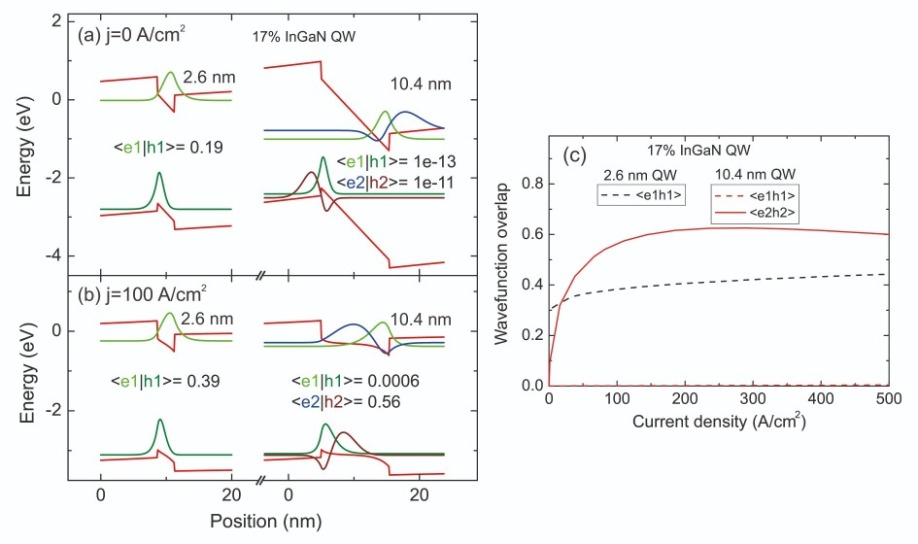
Figure 1. Calculated band structure of a thin (2.6 nm) and a wide (10.4 nm) In0.17Ga0.83N quantum well (a) without and (b) with excitation. (c) Dependence of wavefunction overlap on current density. Above a current density of 16 A/cm2 the
To our knowledge, this is the first demonstration of a quantum well system that has a zero-probability transition between the ground states, but an extremely high one through the excited states. This situation, caused by the huge difference between the overlaps of the ground and the excited states, results from substantial differences in localization. Despite the screening of the piezoelectric field, ground states are still localized in the triangular part of the quantum well (see Figure 1(b)). In stark contrast, the excited states, which have higher energies, fill the entire width of the well. These excited states can be thought of as existing in an almost rectangular quantum well, with small perturbations at the interfaces. In other words, the overlap is almost equal to unity, just like it is in a quantum mechanics textbooks detailing the solutions to a particle in a finite square well.
Testing the theory
Are these findings borne out in practice? To find out, we have produced a portfolio of samples that have In0.17Ga0.83N wells with various widths (the heterostructures are shown in the inset of Figure 2(a)). At high excitation levels that produce excited states, the photoluminescence intensity increases, as predicted (see Figure 2 (a)).
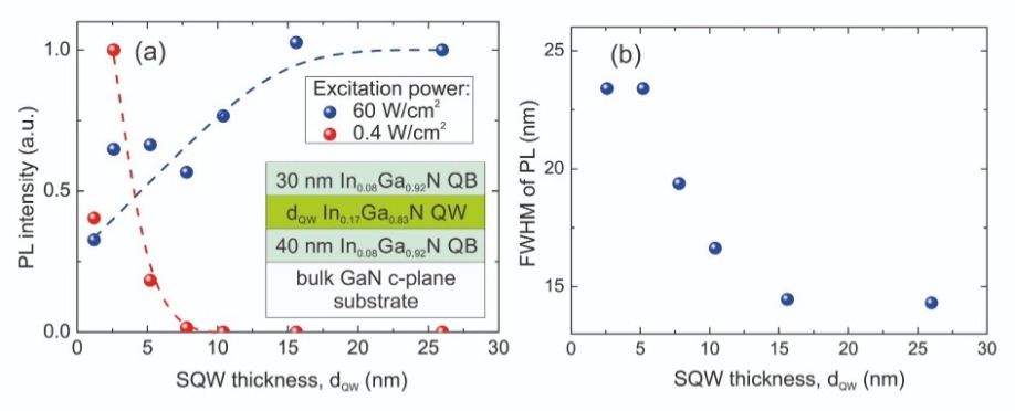
Figure 2. (a) Dependence of photoluminescence intensity of the quantum well thickness for two excitation powers. The inset shows the structure of samples. (b) Dependence of the full-width at half-maximum of photoluminescence measured at an excitation power of 60 W/cm2.
It is intriguing to know at what point the carrier and the current densities are high enough to fill the excited states and take advantage of their high oscillator strength. At both interfaces of an In0.17Ga0.83N quantum well, sheet charges induced by strain are equal to 1.7x1013 cm-2. Screening these charges requires the introduction of a matching number of electrons and holes in the quantum well. For this to happen, the corresponding carrier density should be equal to 5×1019 cm-3. This is a very high number. To put it into perspective, such a high carrier densities is only seen at very high current densities, such as those found in laser diodes at threshold. But this is true only in the case of thin quantum wells.
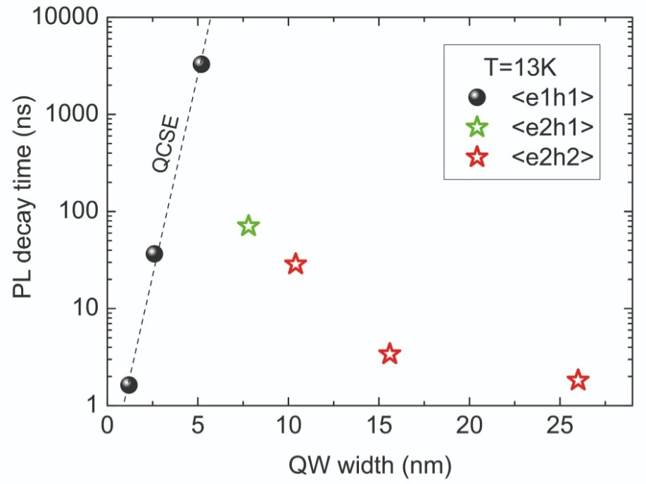
Figure 3. Dependence of photoluminescence decay time on the quantum well width. The legend gives our interpretation of the nature of the observed transition. The dashed line is a guide to the eye, showing the behaviour predicted by a drop of wavefunction overlap with quantum well thickness.
Another benefit of a wider well is that it offers a greater robustness to variations in the quality of the quantum well interfaces. In thin wells, if there are variations in width by just a monolayer, this has a profound impact on the emission profile, including an increase in the full-width at half-maximum. This is a big issue, because unwanted broadening is detrimental to laser diodes, which require as narrow an optical gain as possible. Increasing the thickness of the well has a dramatic impact on the profile of the width of the emission peak. Replacing a well that’s just 2.6 nm-thick with one as wide as 15 nm can narrow the full width at half-maximum for the photoluminescence peak from 23 nm to just 14 nm (see Figure 2(b)).
Measurements of carrier dynamics provide additional proof of the qualitative difference between thin and thick wells. Just a small increase in the thickness of thin wells results in a substantial increase in the decay time of the photoluminescence signal, with values as high as 3 µs observed in 5.2 nm-thick wells. Such a significant increase in photoluminescence decay time is a hallmark of a system with a high dependence of oscillator strength on the thickness of the quantum well (see the region marked with a dashed line in Figure 3). For the 5.2 nm-thick well, the wavefunction overlap for the ground state is calculated to be only 0.0006. When the thickness of the well is increased much beyond this, the decay time starts to drop, with the active region moving into a regime where excited states start to play a major role in recombination.
At longer wavelengths, where the green gap is found, wider quantum wells start to fulfil their true potential. For green-emitting In0.3Ga0.7N wells with a 10.4 nm width, wavefunction overlap can hit 0.63, a value associated with the first excited state (see Figure 4 (a)). This surprisingly high value reveals that the oscillator strength is far higher than that for thin quantum wells.
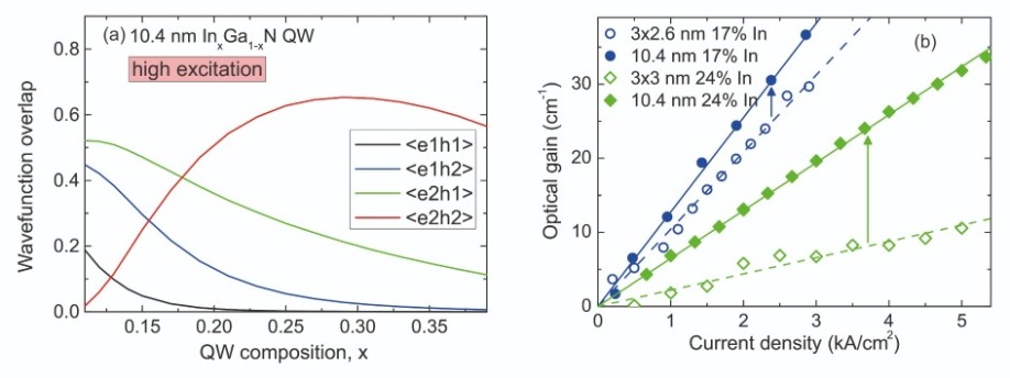
Figure 4. (a) Calculated dependence of wavefunction overlap on quantum well composition. (b) Measured optical gain of four laser diodes with different active region designs given in the legend. Solid and dashed lines are used to extract the differential gain. The arrows indicate the increment realised due to the use of the wide quantum well.
Making lasers
Our efforts at highlighting the benefits of wider wells have included the fabrication of a range of laser diodes, operating in the blue and cyan, at wavelengths of 450 nm and 490 nm, respectively. This portfolio includes lasers with three quantum wells with thicknesses ranging from 2.6 nm to 3 nm, and devices with a single, 10.4 nm-thick quantum well.
Using the Hakki-Paoli method we have measured the optical gain in these devices. This reveals a linear increase with current density (see Figure 4(b)). When the optical gain increases rapidly with current density, this is indicative of either an increase in the efficiency of the quantum well or an increase in the optical confinement factor. Both of these are enhanced with wider wells in the active region. In the case of blue lasers, for the three 2.6 nm-thick wells, the rate at which the optical gain increases with current density is 10.4 cm/kA, but for the single 10.4 nm-wide well, this figure is 12.7 kA/cm. So the shift from three conventional wells to one thicker well delivers an increase in differential gain of 22 percent.
At longer wavelengths, the benefits of wider wells are far greater. Differential gain increases from 2.2 cm/kA to 6.5 cm/kA when switching from three, 3.0 nm-thick wells to a single well that is 10.4 nm-thick. That’s a hike of 195 percent, a significant success that we hope will pave the way to addressing the green gap.
The only major downside of wide wells is that they can exceed the critical thickness of InGaN layers. Due to a high mismatch between InN and GaN, when InGaN alloys are strained to a GaN substrate, defect-free layers can only be grown up to a certain thickness. For the high indium compositions needed to produce green and yellow emitters, data reported for InGaN alloys suggests that it is not possible to produce wide wells with a high quality.
We overcome this issue by turning to plasma-assisted MBE to grow our layers. Using this growth technology, rather than the more common MOCVD, allows alloys of InGaN to be grown at much lower temperatures. It is not surprising that this is beneficial, given that in other semiconductor systems, such as GaN/AlN and germanium/silicon, it is well known that the critical thickness is limited by growth kinetics, and strongly depends on the growth temperature. By using a growth temperature of just 650°C, we have grown layers that are free from dislocations, and have a thickness that is higher than the critical thickness reported for layers grown by MOCVD.
Another advantage of plasma-assisted MBE is that it leads to devices with long lifetimes. Recently we reported laser diodes with a predicted lifetime of up to 100,000 hours. Following that work, we have undertaken preliminary reliability studies on laser diodes with wide wells. Results are very encouraging, with measurements showing exactly the same, extremely low degradation rate. This provides proof that high-quality InGaN layers can be grown with thicknesses that exceed the critical thickness reported for MOCVD growth.
One of our goals for the future is to carry out a comprehensive study on the critical thickness of InGaN layers that are grown by plasma-assisted MBE, and compare our findings to alloys grown by MOCVD. By expanding the limits of InGaN growth, we will allow engineers to turn to wider wells in many different devices, a move that may lead to new applications for this material system.
We also plan to investigate the possibility of bandgap and piezoelectric polarization engineering in wide quantum wells. Up until now, we have restricted our investigations to step-like, wide quantum wells. By turning to variations in the gradient of the InGaN alloy, we can introduce three-dimensional fixed charges, induced by constantly varied strain. This new degree of freedom will enable a further hike in the oscillator strength of the excited states, opening the door to even better lasers and LEDs.
The first growth of AlScN by MOCVD could pave the way to the manufacture of power and RF transistors delivering unprecedented performance.
By Stefano Leone and Michael Mikulla from THE Fraunhofer Institute for Applied Solid State Physics IAF
Demand has never been greater for high-efficiency transistors. They are needed in power electronics, to produce efficient voltage-inverters and serve in hybrid and electric vehicles; and they are needed in the RF domain, to trim the power that is consumed in mobile communication networks.
The leading commercial transistor in all these areas is the AlGaN-based HEMT. Compared with its well established silicon rival, it is a superior device for delivering high power, even at high frequencies, thanks to its superior efficiency and greater compactness.
However, it’s not the ultimate nitride – as further improvements are possible by turning to AlScN. Best known today for its use in radio-frequency filters for the mobile communication market, AlScN features a very high spontaneous polarization that promises to enable the production of devices that handle extremely high currents while operating at very high switching frequencies and withstanding very high electric fields.
These attributes allow an increase in the power density per chip, even while operating at high temperatures. In addition, power modules that employ AlScN components will deliver a step-change in size while drawing less energy, despite an increase in output power, and will be able to fulfil the demand for sustainable, faster, more-efficient electronics.

AlScN layers have a very high crystal quality and the right amount of scandium, making this alloy a strong candidate for next-generation electronic power transistors.
The challenge is to take these results from the lab and develop processes for high-volume, high-yield production in a fab. But that is far from easy. The biggest stumbling block is the growth process. For the vast majority of nitride devices, whether they are LEDs, lasers or transistors, epilayers are grown by MOCVD. However, growing AlScN by MOCVD is very tricky.
Efforts to do so started about a decade ago, when, working independently, researchers at Sandia National Laboratories in the US, and researchers in Tunisia, tried to use this growth technology to deposit GaScN and GaYN. If they had been successful, they would have gone on to try and make LEDs – specifically those in the green wavelength region. Since then, there have been no successful reports of MOCVD growth of scandium-containing nitrides.
The primary difficulties in forming epilayers of this alloy are related to finding an appropriate source material – that is, a precursor – that can be delivered to the reactor in the gas phase. A suitable molecule for scandium is very difficult to find. As the most common scandium precursors have a very low volatility, it is impossible to incorporate relevant amounts of scandium in nitride layers using standard MOCVD equipment.
AlScN could deliver a hike in the performance of nitride materials, improving the characteristics of devices in the high-power and high-frequency electronic markets.
Due to the strong appeal of MOCVD, our team at the Fraunhofer-Institute for Applied Solid State Physics IAF in Freiburg, Germany, has taken another look at whether the difficulties of AlScN growth by MOCVD can be overcome. It can, by modifying the MOCVD process.
Cranking up the temperature
Our group is able to draw on decades of experience in the epitaxial growth of III-V semiconductors, especially nitrides. Our expertise ranges from hardware design to the deposition of very complex epitaxial heterostructures.
Sheet resistance map of an AlScN/GaN HEMT structure deposited on a 100 mm sapphire wafer. The average sheet resistance is 197 Ω/square, with a standard deviation below 1 percent.
Since then, we have passed many milestones. Following several months of testing, we can now produce the alloys we intend to, which incorporate 20 percent to 30 percent of scandium. And thanks to the great experience of the structural characterisation team, we have uncovered the optimum growth conditions for forming the pure wurtzite phase of AlScN. Our focus is now on improving material quality and purity, as well as increasing the productivity of the epitaxial growth process.
The progress that we have made has led us to file a patent application for the growth of materials by MOCVD, using precursors with very low volatility. We hope that the design that we have developed will be very useful to the manufacturers of MOCVD equipment, and that some of them will soon adopt it in their tools. If they do, this could increase the number of researchers that work with AlScN in laboratories and industries.
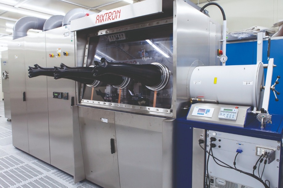
The MOCVD system at Fraunhofer IAF has been modified by the research group to enable the growth of AlScN with sufficient quality and productivity for industry.
While these values are encouraging, far better results are possible by improving crystal quality. In particular, we want to reduce the roughness of our epitaxial heterostructures. The roughness is still higher than typical AlGaN/GaN structures. In addition, we will look to improve the purity of the AlScN layers, as they have high carbon and oxygen levels – these impurities may be detrimental to HEMT structures and other applications. One of today’s projects is to test various growth parameters and see if they can improve the quality of the AlScN epitaxial layers.
A goal for the future is to try and identify new precursors. We expect that by using different ligands in the scandium precursors we can enhance the volatility of this material, and ultimately increase the growth rate from its current value of only 0.1 µm/h. A hike in the growth rate is required before the process can be transferred to multi-wafer MOCVD reactors and used for high-volume production. Before that can take place, it is essential to investigate the impact of different precursors on the purity of the layers.
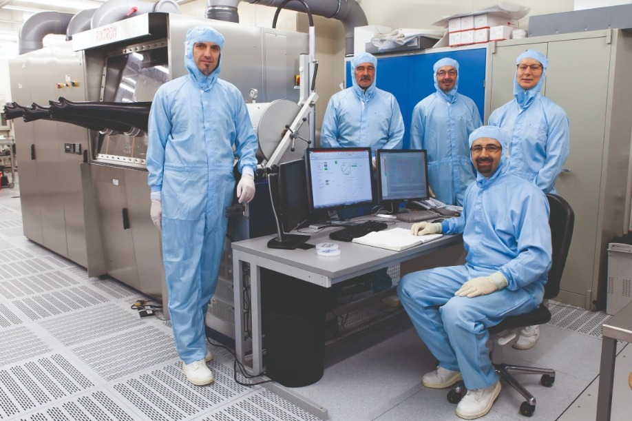
Scientists at Fraunhofer IAF are the world’s first to report the production of aluminium scandium nitride via MOCVD.
There are many great opportunities for AlScN. It has the potential to be the leading material in power and high-frequency electronics, serving in radar, inverters for photovoltaics, and in inverters and converters in electrical vehicles.
But that’s by no means the limit for the use of AlScN. It can feature in filters for 5G, where it can deliver higher performance, thanks to high electromechanical coupling of AlScN. When this is used in electroacoustic components, such as surface acoustic wave, bulk acoustic wave and other types of resonators, magnetron sputtering can deposit films of sufficient quality. This technique, which we have even employed in our institute, has been used to make commercial RF front-end components that have alloys containing scandium. However, if MOCVD is used, the quality of the AlScN layers is better. What is not clear is how valuable this improvement is, and how a switch from sputtering to MOCVD will impact the cost of the filter, and its competitiveness in the market place.
Another amazing property of AlScN is its high degree of ferroelectricity. This attribute could see it adopted in mass storage devices, micro-mechanic actuators, and non-linear optical devices. HEMTs that are made with AlScN can be benefit from its ferroelectric characteristics, as this could allow the reduction in short-channel effects in ultra-scaled transistors, and even enable this device to switch, by using an electric field to invert the polarity of the AlScN barrier layer.
There are further opportunities for AlScN-based materials in optoelectronics. According to theoretical calculations, alloying GaN with ScN and YN can double the internal quantum efficiency of LEDs. If these alloys are used to make efficient multi-quantum wells emitting in the green, this could be a solution to the ‘green gap’, a spectral domain that is not well served by InGaN-based and AlGaInP-based LEDs.
Last but not least, the capability to grow AlScN by MOCVD could enable the growth of other ‘exotic’ materials that have, up until now, only been investigated in research laboratories. It is possible that nitride magnetic materials, such as the nitrides of gadolium and europium, could be manufactured with a similar setup to ours.
While we continue to explore the possibility and potential of AlScN, we are actively searching for research and industrial partners to increase the work undertaken on scandium-containing nitrides. This alloy has great potential, and there is still much to investigate and discover. The exciting journey has only just begun.
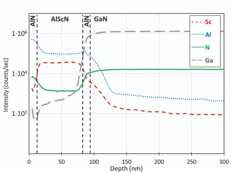
SIMS analysis of a 70 nm-thick Al0.7Sc0.3N layer deposited on a GaN/Al2O3 template with a 10 nm-thick AlN spacer and a 5 nm AlN cap.
T. E. Kazior et al. presented at IEEE/MTT-S International Microwave Symposium, Boston, USA, 2019.
A. J. Green et al. IEEE Electron Device Lett. 40 1056 (2019)
M. T. Hardy et al. Appl. Phys. Lett. 110 162104 (2017)
K. Frei et al. Jpn. J. Appl. Phys. 58 SC1045 (2019)
S. Leone et al. Metalorganic chemical vapor deposition of aluminium scandium nitride , DOI: 10.1002/pssr.201900535.
Lead Image : Photo by Simon Hönl
BY PHILIPP STAUDINGER, KIRSTEN MOSELUND AND HEINZ SCHMID FROM IBM RESEARCH
When device performance is not good enough, researchers wrack their brains, trying to figure out a way to deliver a substantial improvement. Radical approaches often appeal, such as replacing the existing material system with another. This can pay dividends, as has been shown in the space solar cell market, where a switch from silicon cells to those made from multiple junctions, featuring germanium, InGaAs and InGaP, has delivered a boost in efficiency.
But there is another, more subtle approach, also with much promise. Rather than discarding the material system, it can be modified by transforming its crystalline phase. In this way the physical properties of an abundant, well-studied semiconductor can be fine-tuned, while making only minimal changes to its chemistry, which provides the advantage that established fabrication technology can still be used in existing fabs. This is the approach that we are pursuing at IBM, where we have broken new ground by developing novel processes to control the crystal phase in planar films.
In order to appreciate the advances that we have made, it is critical to grasp the basics of crystal structures in semiconductors. Fortunately, this is not too hard, as there are only two predominant crystal symmetries to consider. These are the cubic and hexagonal forms. Note that for elemental semiconductors they are referred to as diamond and lonsdaleite, while for compounds, zinc-blende and wurtzite are used, respectively (see Figure 1).
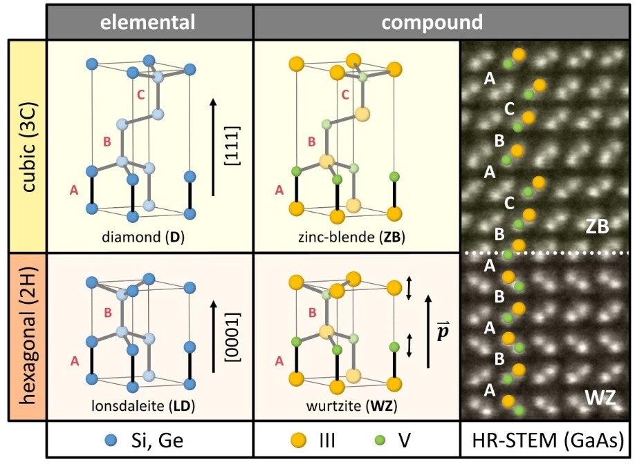
Figure 1. The difference between the cubic (3C) and the hexagonal (2H) crystal symmetries is defined by the atomic bilayer stacking along the [111] or [0001] direction. The corresponding phases are called diamond and lonsdaleite for elemental semiconductors, and zinc-blende and wurtzite for compound semiconductors. The loss of symmetry combined with the ionicity results in spontaneous polarization effects in wurtzite semiconductors, which are absent in other symmetries. A high-resolution scanning transmission electron microscopy image reveals the zinc-blende and wurtzite configurations of GaAs, and shows that a transition between these two phases is possible along the stacking axis.
When nanostructures are grown along this direction, switching the stacking order introduces a different crystal phase – and ultimately creates a new type of metastable material. This principle is illustrated in a high-resolution scanning transmission electron microscopy image of polymorphic GaAs (see right hand side of Figure 1). Note that this type of phase transition, involving a metastable state, is often observed in nanowires. It stems from their low-dimensional character, and the strong role that surface energies exert during epitaxial growth.
Metastable merits
Until recently, metastable crystal phases have often been viewed as just a curiosity of nanowire growth. But now they might potentially provide solutions to some of the biggest problems associated with compound semiconductor devices. In conventional GaN LEDs, which have a wurtzite crystal structure, radiative recombination is impaired by strong internal fields that are responsible for the quantum confined Stark effect. Switch to the cubic phase, and these fields go away, helping to bridge the ‘green gap’ – a wavelength range in the centre of the visible spectrum that so far lacks efficient emitting materials.
Another promising solution to address the green gap is to use metastable wurtzite III-phosphides, as this class of III-Vs offers an extended tuneable direct bandgap throughout the visible spectrum in contrast to their stable counterparts (see Figure 2). Equally exciting is that germanium and germanium-rich SiGe compounds become direct bandgap semiconductors in their metastable lonsdaleite phase. This could open the door to CMOS-integrated light sources for on-chip optical communication.
These opportunities highlight the promise that crystal phase tuning has, to deliver a profound impact on many sectors within our industry, including electronics and solid-state lighting. Progress is not easy, however, as growth of metastable phases is extraordinarily challenging. For too long, success has been limited to thin nanowires, which are notoriously difficult to turn into devices, hampering scientific and commercial exploitation. What’s needed are technologies that will enable the synthesis of these materials in sizes and form factors that are compatible with conventional processing techniques.
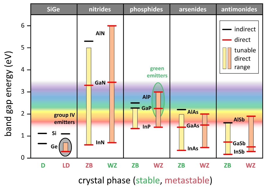
Figure 2. Bandgap energies of common semiconductors differ in their stable and metastable phase. For each semiconductor, the left side depicts the cubic phase, and the right side the hexagonal phase. Except for nitrides, the cubic phase is thermodynamically preferred. The hexagonal symmetry generally offers a wider range of direct bandgaps. Silicon is an exception, staying indirect even in the lonsdaleite phase. Crystal phase tuning offers an extended range for wurtzite III-phosphides throughout the visible spectrum and a direct group IV lonsdaleite SiGe compound for compositions of up to around Si0.35Ge0.65.
Over the years, many groups have investigated different techniques for producing metastable material using either MBE or MOCVD. In general, these approaches are based on the transfer of the crystal phase from a substrate to an epilayer, which – under the right conditions – forces the layer to adopt its metastable form. The downside of this approach is that there are no appropriate substrates with lattice constants that are suitable for the materials of interest. Consequently, these films tend to be plagued by large defect densities, making them unsuitable for device applications.

From nanowire to film growth
We are taking a different approach, based on novel epitaxial techniques that build on the knowledge of nanowire growth. Our aim is to produce high-quality metastable films, which provide a platform for robust material characterisation and device fabrication.
Our success comes from exploring a range of strategies. Initially, we studied selective-area epitaxy. Although this did not produce metastable layers, it did provide a foundation for more elaborate methods, making use of either a zipper-like growth mode or confinement under a top oxide (see Figure 3 for details).
Progress has come from the use of conformal epitaxy, which is described in more detail in Figure 4. Our starting point is a conventional zinc blende III-V substrate that is patterned in lines, using an oxide mask. Sacrificial etching defines hollow cavities, which have openings on their extremities to allow growth species to diffuse inside. MOCVD is employed for this, as it allows selective nucleation in the centre of the template. After this, the growth of the crystal is guided within the cavity.
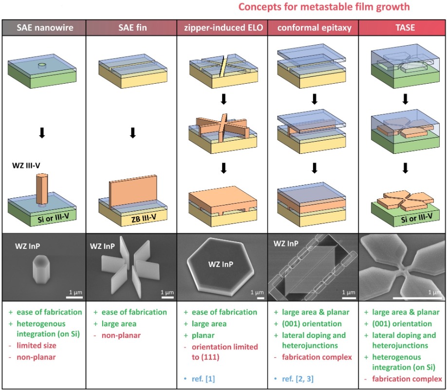
Figure 3. Several strategies can be used for wurtzite epitaxy, from nanowire to film growth. Selective-area epitaxy (SAE) of nanowires and fins allows for a phase change along the vertical stacking axis. The team at IBM have used this principle as a basis for other more elaborate techniques to obtain planar films. Connected fins can result in a zipper-induced epitaxial lateral overgrowth, as detailed in [1]. Conformal epitaxy makes use of a physical layer confinement, realized via an oxide layer on top of the seed line. This enables the use of standard (001) oriented substrates [2, 3]. Starting growth from a small seed additionally allows for direct growth on silicon wafers, accomplished by template-assisted selective epitaxy (TASE). Such an approach also allows for the growth of more advanced geometries, rather than just layers.
Last but by no means least, our technology allows us to choose the geometry of the crystal through the design of the cavity. As well as being able to produce a flat top surface, which is compatible with standard film processing techniques, we can produce geometries beyond simple rectangles, such as those that form optical resonators. The lateral growth direction further opens up the opportunity for in-plane integration of heterostructures and offers great promise for device fabrication.
Going big
While there is much to admire about conformal epitaxy – it offers control over growth conditions and substrate orientation, and has additional advantages, such as lateral doping profiles and the co-integration of multiple materials – it does have its drawbacks. Its biggest weakness comes from its elaborateness.
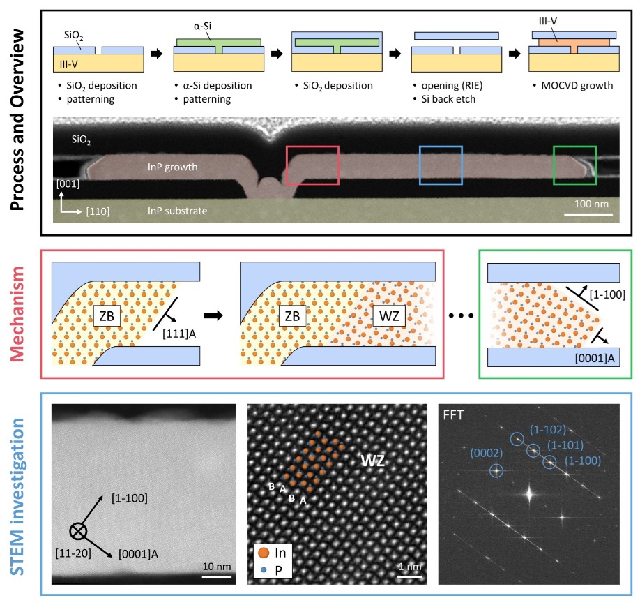
Figure 4. The team at IBM have used conformal epitaxy to produce metastable films. Processing steps involve a sacrificial material – typically amorphous silicon – to form an empty oxide cavity on top of a III-V wafer. Subsequent selective epitaxial growth in the cavity, using MOCVD, can then proceed, starting from a line opening in the oxide. A cross-sectional, false-coloured, scanning transmission electron microscopy image shows a typical InP structure with a dip on top of the line seed that results from processing. Coloured rectangles, showing areas of interest, are described in more detail. In the first section of the grown material, pure zinc-blende material is obtained, mirroring the crystal structure in the substrate, because epitaxy follows directions other than the stacking axis of the atomic bilayers. Once the [111] facet is formed, a phase transition can take place under the correct growth conditions. This enables a deposition that is similar to fin-growth with a [0001]A growth front and a [1-100] side facet. The bottom row depicts a detailed high-resolution, scanning transmission electron microscopy investigation of the central area. The wurtzite phase can be seen directly in the atomic stacking as well as in a fast Fourier transformation (FFT) image to the right.
We have also pioneered a technique for producing layers in an economical way: zipper-induced epitaxial lateral overgrowth (this is illustrated in Figure 3). This involves selective-area epitaxy on (111)-oriented wafers and delivers a change in the atomic stacking of bilayers along the vertical direction through the use of nanowires and fins. This type of low dimensional nanostructure, illustrated in Figure 5, tends to grow vertically, so it doesn’t expand laterally to form a layer. However, with a small trick, we can create an unstable concave edge during growth. This edge triggers a zipper point, leading to controlled lateral expansion. To do this, we merge, in a central point, line openings with directions that are different but crystallographically equivalent. As the lateral growth direction is perpendicular to the stacking axis, this prevents any additional phase change, ensuring that the metastable material is transferred into a layer.
With this elegant technique we have realised exceptional material quality and phase purity. Photoluminescence measurements, presented in Figure 5, demonstrate that the hexagonally shaped films are optically active. Light is emitted in a spectral domain that has been predicted for the metastable wurtzite phase of InP. Thanks to the robustness of our technique, many individual hexagons can be tiled together to produce a virtually continuous film of metastable material. This highlights the potential of our technology for making large-area virtual substrates, and promises to speed its use in applications.
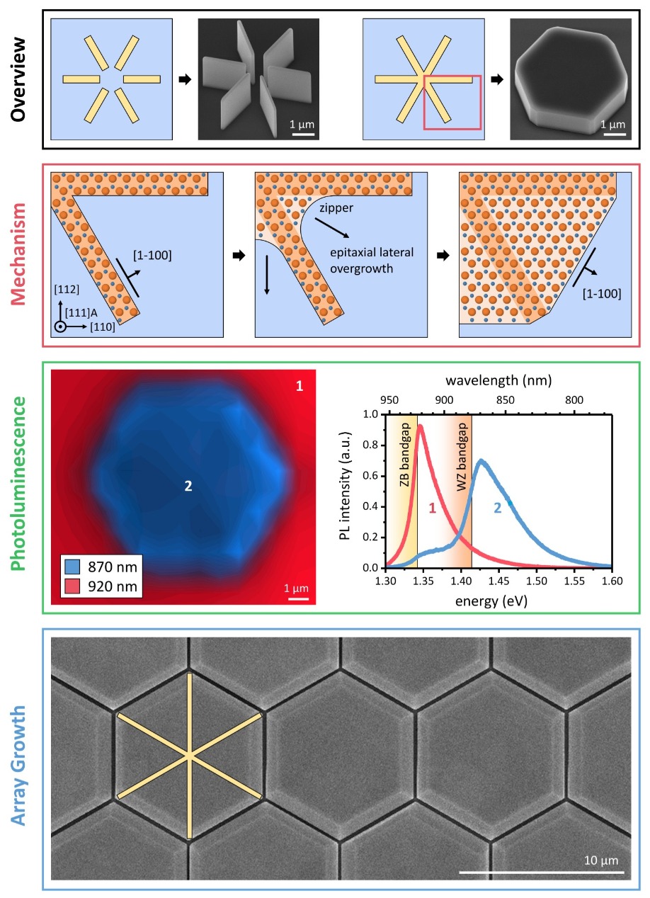
Figure 5. Zipper-induced epitaxial lateral overgrowth is a promising approach to scale the production of metastable films. Connecting the central point of circularly arranged metastable fins induces zipper points at the concave edges. In turn, this triggers epitaxial lateral overgrowth. In this unique epitaxy technique lateral growth continues until stable [1-100] edges are formed, resulting in the formation of hexagonal layers. Scanning micro-photoluminescence measurements reveal the emission difference between the substrate (zinc-blende) and the grown structures (wurtzite), formed in InP. Tiling individual hexagons closely together in an array results in a virtual wurtzite substrate. This can provide a platform for device applications.
The work presented here received financial support from the European Union H2020 program SiLAS (Grant Agreement No. 735008)
Photo by Markus Ritter
Further reading
[1] P. Staudinger et al. Nano Lett. 20 686 (2020)
[2] P. Staudinger et al. Nano Lett. 18 7856 (2018)
[3] P. Staudinger et al. in 2019 Compound Semiconductor Week (CSW) 18, 1–2 (IEEE, 2019)

Omidirectional photoluminescence offers a non-destructive method for measuring the density of carbon contaminants in GaN
Carbon impurities limit the performance of GaN devices. They create deep levels in the material, leading to leakage currents.
To reduce the levels of carbon contaminants, the first step is to quantify this impurity in the nitrides. Unfortunately that’s not easy, because conventional approaches are slow, destructive, and limited in sensitivity. But all these issues can be overcome, according to recent work by a collaboration in Japan between researchers at Tohoku University and SCIOCS.
Spokesperson for this partnership, Kazunobu Kojima from Tohoku University, claims that the team have shown that omidirectional photoluminescence spectroscopy offers a non-contacting, non-destructive, high-sensitivity technique for detecting carbon levels in GaN. Kojima says that even when they examine some of the world’s purest GaN crystals, they can measure their carbon content.
The established approach for determining the concentration of elements in compound semiconductor materials is a destructive method known as secondary ion mass spectrometry (SIMS). Using standard depth profiling, this technique has a detection limit for carbon of 3 x 1015 cm-3. This limit falls to 5 x 1014 cm-3 by switching to a raster change approach.
In comparison, the limit for omidirectional photoluminescence spectroscopy is far lower. A conservative estimate is 1014 cm-3.
Another strength of omidirectional photoluminescence spectroscopy is its capability to detect very deep levels formed by point defects. “[These levels are] too deep to detect by deep-level transient spectroscopy, a popular method to detect impurity and defect levels in semiconductors,” says Kojima.
The team have studied six samples – four grown by MOCVD, and the other two by HVPE. Measurements with a SIMS tool with a detection limit of 7 x 1014 cm-3 reveal that these samples provide a range of carbon impurities. One of the HVPE-grown samples has a carbon concentration below the detection limit, another a value of 2 x 1016 cm-3, and MOCVD-grown materials have values between 3 x 1015 cm-3 and 4.3 x 1015 cm-3.
In addition to measuring the external quantum efficiency of the samples, Kojima and co-workers have calculated the internal quantum efficiency by using a streak camera to record the photoluminescence lifetime.
Under excitation, the GaN samples produce photoluminescence over wavelengths ranging from 1.5 eV to 3.5 eV. For the near band-edge emission, which is related to carbon impurities, both the internal and external quantum efficiencies monotonically increase with carbon concentration (see figure). As the near-band edge external quantum efficiency is only 1 percent at a carbon concentration of 4 x 1014 cm-3, it is possible that concentrations below 1014 cm-3 could be measured with this technique.
Measurements of photoluminescence lifetime show that this decreases from 0.78 ns to 0.32 ns as the carbon concentration falls from 2 x 1016 cm-3 to 3 x 1015 cm-3. For lower concentrations, the photoluminescence lifetime plateaus. To try and understand the reason for this, Kojima and co-workers have plotted the radiative and non-radiative lifetimes as a function of concentration – the former has a steady increase with concentration, while the latter mirrors the photoluminescence lifetime. This led the team to postulate that samples contain vacancy-related intrinsic non-radiative recombination centres, with an estimated density of 2.1 x 1015 cm-3.
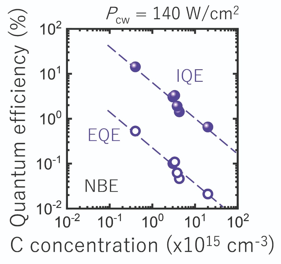
Internal and external quantum efficiencies of near band edge (NBE) photo-luminescence provide a method to measure carbon concentrations in GaN.
K. Kojima et al. Appl. Phys. Express 13 012004 (2020)
Sandwiching HfO2 between two layers of Al2O3 improves the performance of buried InP MOSFETs
Engineers from China are claiming to have improved the performance of buried-channel InP MOSFETs by setting a new benchmark for the quality of the gate dielectric.
This success – by the team from Guilin University of Electronic Technology and the Chinese Academy of Sciences, Beijing – will aid the development of InP MOSFETs, which are very important devices for making millimetre-wave ICs.
One of the downsides of conventional InP MOSFETs is that when reduced to the nanoscale, severe gate leakage results, along with a compromised breakdown voltage.
“Buried InP MOSFETs can solve these problems through applying high-k gate dielectrics, without losing the advantage of high channel mobility,” argues team spokesman Honggang Liu from the Chinese Academy of Sciences.
Unfortunately, burying the channel introduces its own problems, as the barrier above it makes it far more challenging to control gate voltage.
The solution is to decrease the equivalent oxide thickness of the gate oxide layer. However, this must be accomplished without resorting to a thin, high-k layer that leads to poor interface quality, introduces bulk defects, and ultimately results in poor transport in the channel and a large leakage current.
Addressing all these concerns are the laminate dielectrics produced by Liu and co-workers. They feature a layer of HfO2, sandwiched between two layers of Al2O3.
Liu claims that by optimising process conditions, the team has realised the lowest density of interface states between InP and a high-k dielectric. “The lower the density of interface states, the better the device performance.”
The team illustrate the superiority of their laminates over simpler designs by measuring the performance of a range of MOS capacitors and MOSFETs.
MOS capacitors have been made by taking n-type InP substrates with a doping concentration of 5 x 1015 cm-3, chemically cleaning and passivating their surface, and adding a variety of gate structures – single layers of Al2O3, stacks of this oxide and HfO2, and laminates made from a layer of HfO2, sandwiched between two layers of Al2O3.
Measuremnets on these capacitors revealed that a top layer of Al2O3 in the laminate trimmed the leakage current, reducing it by an order of magnitude compared with just the pairing of Al2O3 and HfO2.
Further proof of the strength of the laminate came from measurements of 100 nm gate length buried In0.25Ga0.75As MOSFETs. One had a 3 nm Al2O3 gate dielectric, another a 3 nm-thick layer of HfO2 sandwiched between two layers of Al2O3 – a 0.8 nm-thick layer on top of the InP, and a 0.5 nm-thick layer on top of the HfO2.
The MOSFET with the laminate produced a drive current of 149 mA mm-1, for a gate-source voltage that is 0.8 V above threshold and a drain-source voltage of 0.6 V. At identical conditions, this current is 38 percent higher than that of the MOSFET with just the Al2O3 gate dielectric.
Switching to the laminate gate also improves transconductance. It’s value of 261 mS mm-1 at a drain-source voltage of 0.6 V is 41 percent higher.
One of the goals for the team is to see if the superior gate will enable highly scaled versions of these MOSFETs to produce higher power gain in the terahertz domain.
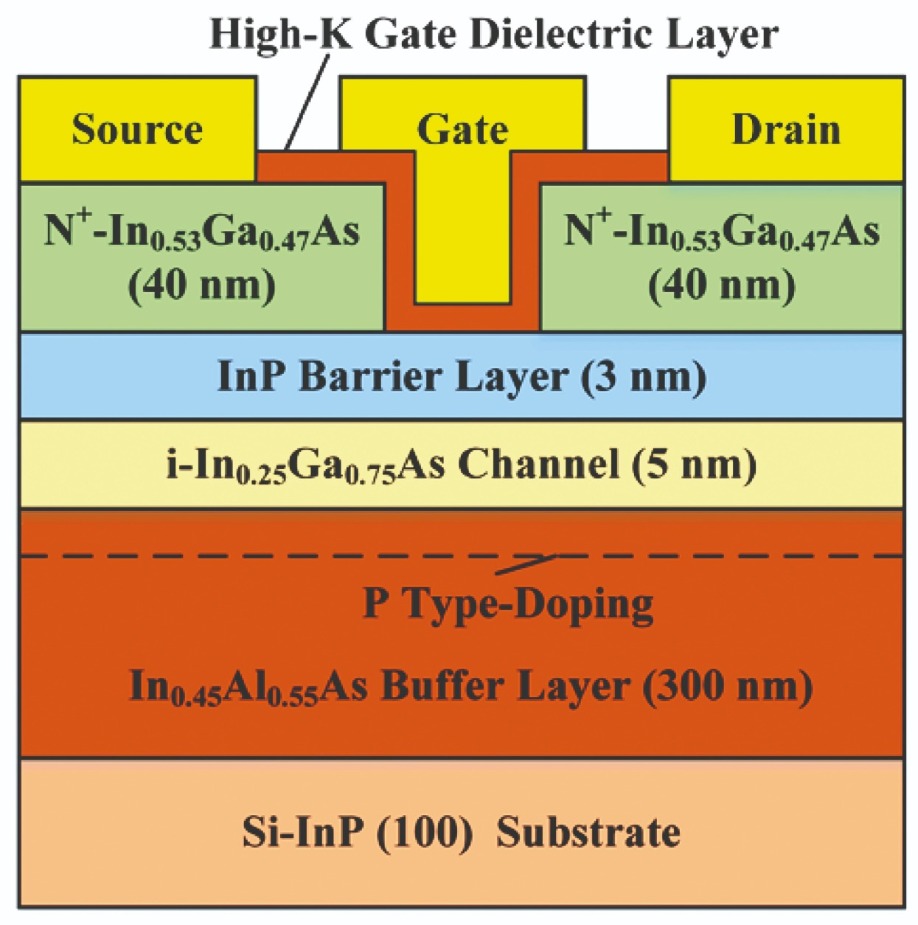
MOSFETs can deliver a higher drive current and superior transconductance when they employ a gate formed from a 0.8 nm-thick layer of Al2O3, followed by a 3 nm-thick layer of HfO2 and a 0.8 nm-thick layer of Al2O3.
Y. Li et al. Appl. Phys. Express 13 011004 (2020)
Inserting an underlayer beneath the active region supresses alloy fluctuations and non-radiative recombination centres
Most commercial LEDs employ an underlayer beneath the active region to improve the efficiency of this device and trim its operating voltage.
The reasons behind these two improvements are not well understood, so researchers from Japan have investigated this matter, finding that these gains come from reductions in non-radiative recombination centres and alloy fluctuations.
Spokesman for the team, Dong-Pyo Han from Meijo University, says that their most important insight is that there is a strong interplay between the non-radiative recombination centres and the alloy fluctuations on the efficiency of green LEDs. “The inter-relationship is very critical to determining the internal quantum efficiency and the voltage efficiency in long-wavelength LEDs.”
The magnitude of the impact of non-radiative centres and alloys fluctuations is discussed in a Physical Review Letters paper from 2016, written by researchers from the University of Rome Tor Vergata, CNR-ISMN, and the University of Bremen. This European collaboration also considered the quantum confined Stark effect and Auger recombination, and found a degradation of 15 percent in the internal quantum efficiency of 510 nm LEDs associated with non-radiative centres and alloys fluctuations.
An optimal interlayer could address both of these energy-sapping mechanisms, and allow the maximum internal efficiency of 510 nm LEDs to climb to 70 percent.
To study the impact of the interlayer, the team investigated two conventional LEDs structures with active regions containing five 3 nm-thick In0.24Ga0.76N quantum wells. One of these devices also featured a 30 nm-thick underlayer of silicon-doped In0.06Ga0.94N and a 10 nm-thick spacer layer.
Plots of the influence of drive current on the light output power, the internal quantum efficiency and the drive voltage revealed that the addition of the underlayer produced a substantial improvement in LED performance (see figure).
The team went on to determine the Shockley-Read-Hall recombination coefficient and the radiative recombination coefficient by combining values for internal quantum efficiency with differential carrier lifetimes. The results suggest that adding an underlayer to a green LED decreases the density of non-radiative recombination centres in the active region and increases the non-radiative recombination rate.
Further insight into the impact of the underlayer came from capacitance-voltage measurements, which reveal the depletion width. These measurements showed that the underlayer led to an increase in depletion width at zero bias, and resulted in more of the quantum wells exhibiting extrinsic properties.
Han and co-workers offer a model to explain this. They argue that the drop in growth temperature when transitioning from GaN layers to the active region reduces the formation energy of surface defects, such as nitrogen vacancies. These surface vacancies then penetrate into the quantum wells and incorporate with indium atoms to create non-radiative centres. However, when an underlayer is present, this captures the majority of surface defects.
Micro-photoluminescence revealed that the addition of an interlayer produces a switch from localised emission from dots with diameters from around 50 nm to 2 µm to a relatively uniform dot diameter from 0.5 µm to 1.5 µm. This difference can be explained by the interlayer reducing fluctuations in alloy composition.
Efforts by the team are now focused on understanding the relationship between the quantum-confined Stark effect, non-radiative recombination centres and alloy fluctuations. “We believe this effort can provide a hint to overcome the green gap,” says Han.
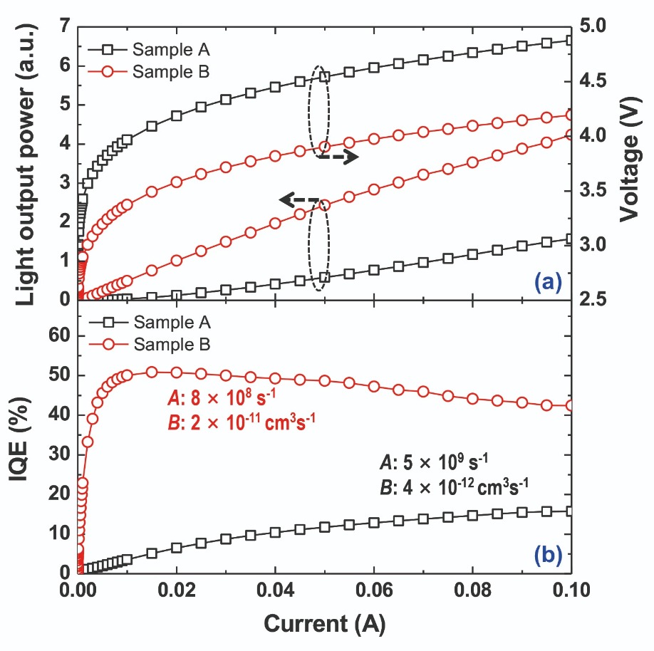
Samples A and B are LEDs that are identical, apart from the latter having an underlayer. At a 50 mA drive current, this addition produces an increase in output intensity by a factor of 4.6, a reduction in operating voltage from 4.54 V to 3.90 V, and a 4.5-fold hike in internal quantum efficiency
D.-P. Han et al. Appl. Phys. Express 13 012007 (2020)