André Richter, Sergei Mingaleev and Igor Koltchanov of VPI Photonics discuss the power of a layout-aware schematic-driven design methodology for accelerating the application of integrated photonics.
Motivation
Despite impressive advances in integrated photonics technologies, costs associated with the design and fabrication of photonic integrated circuits (PICs) are still several orders of magnitude higher than those for their microelectronic counterparts, which limits the rapid application of PICs in many areas. The need to reduce these costs has been a major driving force for integrated photonics development during the past few years. So why not directly adopt the well-proven methodologies from electronic design automation (EDA)? While similar to electronics, the key for cost reduction lies in the introduction of standardized process design kits (PDKs) and a generic foundry model. However, recent design trends show that dedicated photonic design automation (PDA) tools – closely integrated with EDA tools – are necessary to address the specific PIC design needs.
The fundamental difference between the design processes for photonics and electronics is caused by the double nature of optical waveguides. In some cases, they just route optical signals between building blocks (BBs), comparable to electrical wires in electronic circuits. This is when waveguide properties might not be important. In other cases, however, waveguides determine interference conditions between signals in different optical paths. Their properties are of crucial importance in such cases and should be known and already taken into account at the start of the circuit design. Unfortunately, there is no clear separation between those two types of cases. As the designed PIC grows, adding new couplers between reflective parts may turn any connecting waveguide into a functional one. Functional waveguides often serve as connectors of other components, so their dimensions are restricted not only by the desired functions, but also by the geometrical requirements of an adequate layout connectivity. Consequently, the PIC design process cannot be separated so easily into two distinct stages as is possible in the case of electronic circuit design. This is outlined in more detail below.
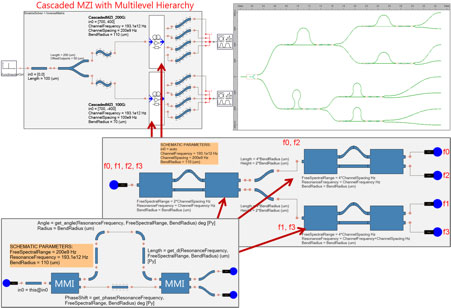
Utilizing the standard schematic-driven design approach, the circuit layout is fully determined by the connectivity between ports of neighboring PDK BBs, which requires that the layout of any individual BB is completely defined by its parameters. This allows circuit simulations of the designed PIC to be performed immediately, since the compact simulation model of each BB is known at any design step. However, due to the twofold nature of optical waveguides in PICs this approach is often not feasible. For instance, even the design of a simple Mach-Zehnder Interferometer (MZI) with a given free-spectral range (FSR) around a nominal center frequency sets a number of functional and geometrical design requirements on the two optical waveguide arms forming the MZI, which leads to deriving and solving a cumbersome set of nonlinear equations. In practice, attempts to design more or less complex PICs employing the standard schematic-driven design approach can result in very time-consuming back and forth iterations between the circuit simulator and layout tool. Moreover, design tasks such as device performance and yield optimization cannot be automated and thus become merely unmanageable.
For a number of applications, the problems outlined above can be solved by employing a layout-driven design approach. For example, dedicated photonic layout design tools (such as OptoDesigner by PhoeniX Software and IPKISS by Luceda) provide advanced scripting capabilities with support of an easy netlist-based PIC design process and immediate access to relative and absolute locations of any BB ports inside the circuit netlist. Moreover, they provide advanced routing capabilities, including support of elastic waveguide connectors. However, accurate and efficient simulation of modern large-scale PICs with a mix of passive and active BBs requires development of complex specialized circuit simulation engines. That is why the layout-driven design approach should include a separate stage for the simulation of the designed PIC with a dedicated photonic circuit simulator. But simulations of complex non-passive circuits require embedding the designed PIC into a complex simulation framework: adding properly configured electrical and optical sources, post-processing of output signals with specialized instrumentation tools, and visualization of obtained results. Consequently, designers need again to frequently switch between a layout design tool and circuit simulator, and experience serious difficulties trying to organize automated sweeps over layout parameters or perform automated design optimization.
Layout-aware schematic-driven design methodology
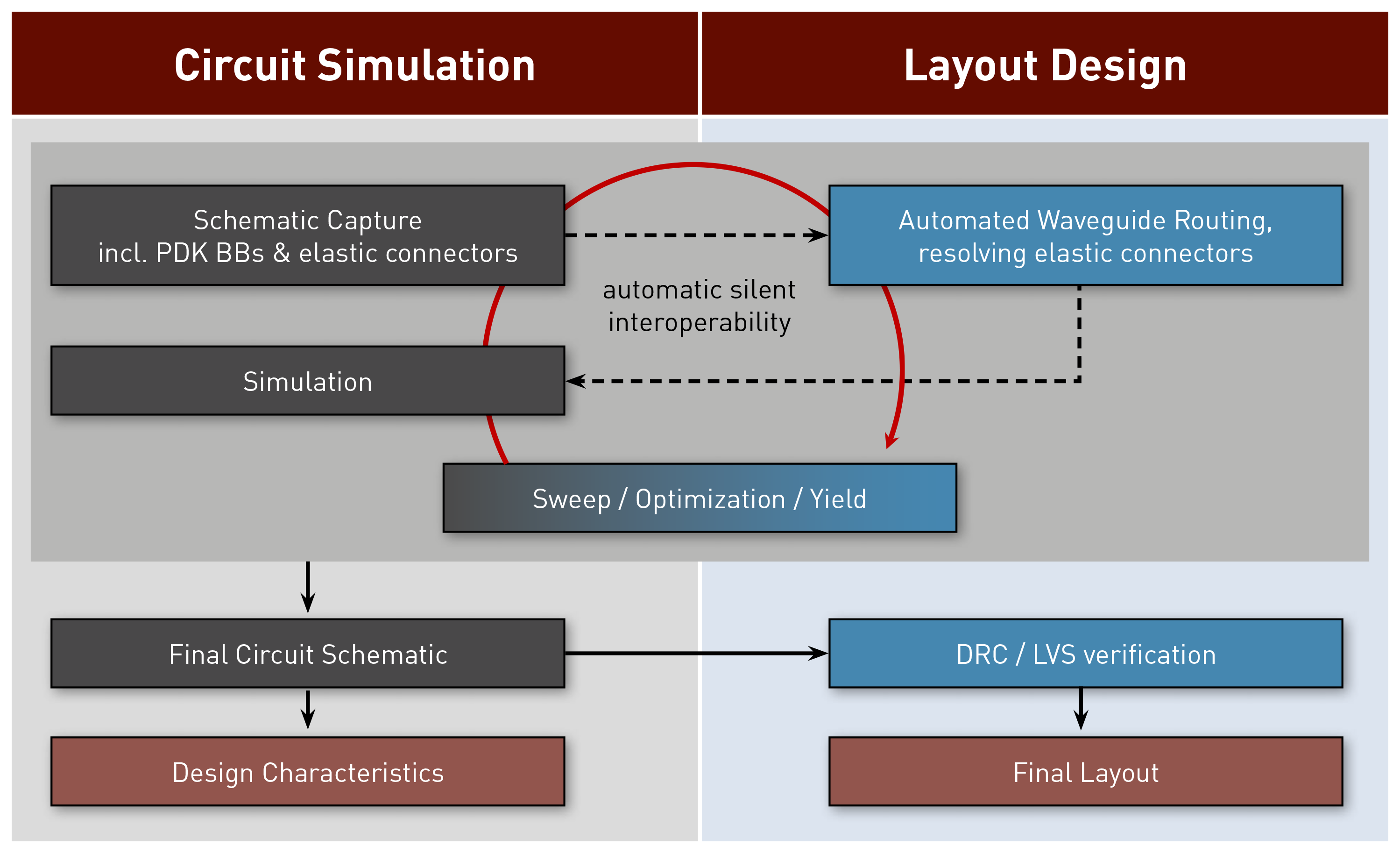
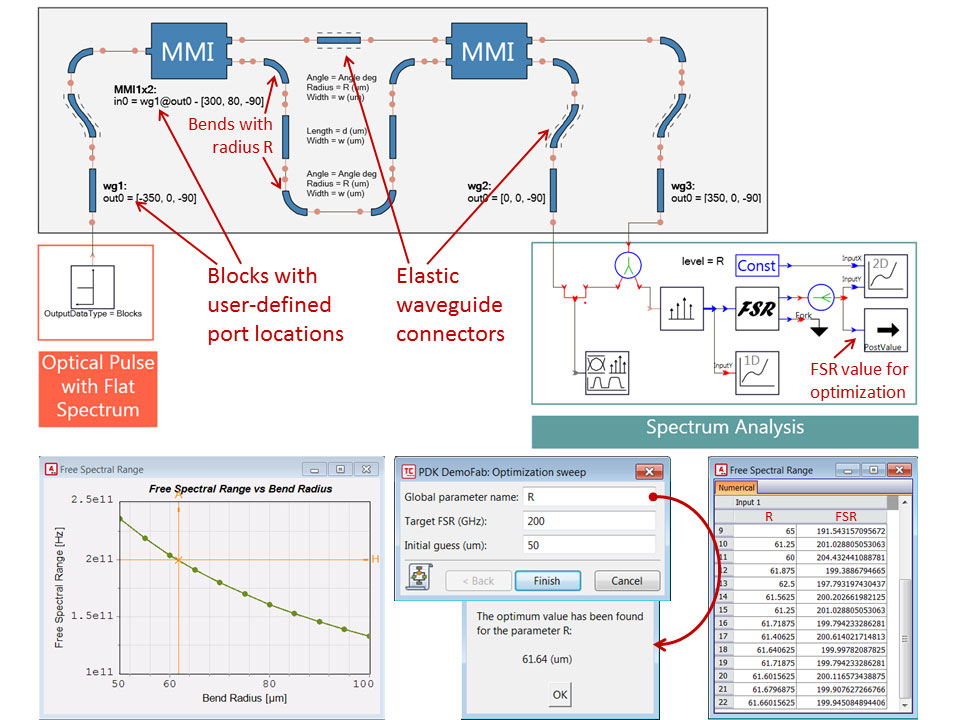
The layout-aware schematic-driven design methodology [1] represents an efficient practical solution to the issues outlined above, as it allows circuit simulation and layout design tasks to be performed simultaneously, using the same schematic capture environment. For this, a circuit-level simulator is seamlessly integrated with a layout design tool, providing designers transparent access to the capabilities of both software packages, as illustrated in Fig. 1. In particular, it becomes possible to directly specify in the circuit-level simulator physical locations and orientations of PDK BBs on the final layout. Also, the library of PDK BBs is extended with a set of elastic waveguide connectors (the same as provided by the underlying layout design tool), allowing sub-circuits having fixed locations to be easily interconnected without the need to manually solve complex geometrical problems. The circuit simulator automatically, and invisibly for users, invokes the layout design tool to determine the actual physical lengths and shapes of all elastic connectors, constructs compact simulation models for them, and after that initiates the circuit simulations. This allows the combination of graphical schematic capture, layout design with automated waveguide routing, and circuit simulations, which are currently considered separately representing a major problem for PIC designers.


