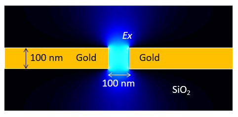
The above schematic shows a photonic waveguide based on plasmonics on an Si photonic platform. The optical field is confined in a 100-nm-wide gap between two metallic plates. By filling this gap with electro-optic (EO) polymers and applying voltage to these metallic plates, we can change the refractive index of the EO polymer. Thus, we can construct a very compact optical phase shifter, which is a fundamental element of optical modulators.
Recently, such a plasmonic-polymer waveguide system has been used to develop Mach-Zhender interferometer optical modulators19. Since the gap is very narrow, the electric field in the gap is very strong and the modulation efficiency becomes extremely high. For example, the voltage-length product -- which is a measure of the efficiency of phase shifters -- reaches 0.006 V.cm, which is less than 1/100 of that of a typical silicon modulator. Thus, a device a few tens of micrometers long can function as a modulator with practical modulation depth, and such a small device can operate at very high frequencies of over 100 GHz. Such plasmonic devices would be a significant breakthrough in the post-Moore photonics technology.
Summary
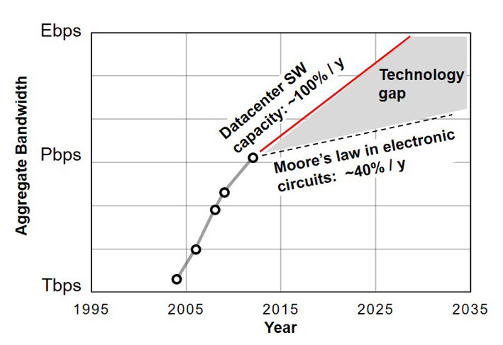
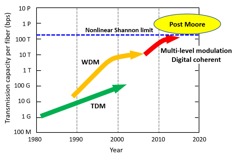
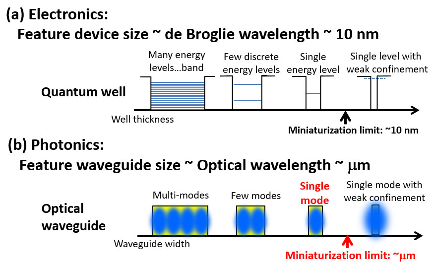
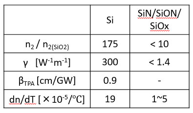
Moore’s Law in data transmission systems is nearing its end, and we need post Moore-photonics technology. In the development of post-Moore photonics technology, we can apply the same approaches that have been established in electronics, and silicon photonics can provide immediate solutions for post-Moore photonics technology. However, we must note here that silicon photonics itself requires post-Moore technology because of the quantum limit in miniaturisation and poor material characteristics. Here again, the same approaches established in electronics are applicable to post-Moore silicon photonics with the help of backend photonics and plasmonics.
Biography
Koji Yamada is head of the Silicon Photonics Group at the Electronics and Photonics Research Institute - a division of Japan's National Institute for Advanced Industrial Science and Technology (AIST). Key themes of his group's work include the research and development of advanced silicon photonics devices.
Web - https://unit.aist.go.jp/esprit/en/research/5_si-photo/si-photo_en.html
References and further reading
[1] A. Singh et al., Proc. annual conference of the ACM Special Interest Group on Data Communications (SIGCOMM 2015), London (2015).
[2] D.J. Richardson, Science 330, 327 (2010).
[3] Y. Urino et al., Proc. ECOC 2013, Mo.4.B.2F, London (2013).
[4] C.R. Doerr et al., Proc. ECOC 2011, Th.13.A.3, Geneva (2011).
[5] M. Usui et al., Proc. ICEP-IAAC 2015, 660-665, Kyoto (2015)
[6] T. Pinguet et al., Proc. IEEE GFP 2012, ThC1, San Diego (2012).
[7] J-M. Fedeli et al., IEEE J. Selected topics in Quantum Electronics 20, p. 8201909 (2014).
[8] J. Kurumida et al., Proc. ECOC 2014, PDP 1.3, Cannes (2014).
[9] K. Tanizawa et al., Optics Express 23, 17599 (2015)
[10] K. Okamoto, Laser & Photonics Review 6, 14 (2011)
[11] T. Tsuchizawa, ”Guided Light in Silicon-Based Materials,” Handbook of Silicon Photonics (ed. by L. Vivien and L. Pavesi, CRC Press, 2013)
[12] T. Hiraki et al., Electronics Letters 51, 74 (2015).
[13] R. Takei et al., Optics Express 23, 18602 (2015).
[14] H. Nishi et al., Applied Physics Express 3,102203 (2010).
[15] T. Hiraki et al., IEEE Photonics Journal 5, 4500407 (2013).
[16] H. Fukuda et al., Optics Express 16, 4872 (2008).
[17] L. Chen et al., Optics Letters 36, 469 (2011).
[18] T. Hiraki et al., Proc. OFC 2015, W1A.2, Los Angeles (2015).
[19] C. Haffner et al., Nature Photonics 9, 525 (2015).


